Phase transition induced vertical alignment of ultrathin gallium phosphide nanowire arrays on silicon by chemical beam epitaxy†
Zhang
Zhang
*ab,
Stephan
Senz
b,
Fuli
Zhao
c,
Lijun
Chen
b,
Xingsen
Gao
a and
J. -M.
Liu
d
aInstitute for Advanced Materials, School of Physics and Telecommunication Engineering, South China Normal University, Guangzhou 510006, China. E-mail: zzhang@scnu.edu.cn
bMax Planck Institute of Microstructure Physics, Weinberg 2 Halle, 06120, Germany
cLaboratory of Optoelectronic Materials and Technologies, Sun Yat-sen University, Guangzhou 510275, China
dLaboratory of Solid State Microstructures, Nanjing University, Nanjing, 210093, China
First published on 8th August 2012
Abstract
We demonstrate high-density heteroepitaxial growth of sub-10 nm diameter gallium phosphide (GaP) nanowire (NW) arrays on silicon (Si), using chemical beam epitaxy (CBE). The vertical alignment of GaP NW arrays is facilitated by an initial phase transition from zinc blende (ZB) to wurtzite (WZ), which is determined based on the observations of a phase transition during the early heteroepitaxial growth for the wires with diameters below 10 nm and the crystallographic structure of the Au–Ga catalyst tip. We propose a new ledge-flow mechanism with a nucleus consisting of three atomic planes (C-B-A stacking) that enables the tilted growth directions of the ZB phase. With photoluminescence (PL), a band-to-band recombination occurs with an energy similar to the indirect band gap of bulk ZB GaP with a short lifetime. The band structure of bulk ZB and WZ GaP was calculated using different approaches.
During the past decade, semiconductor nanowires (NWs) have attracted much attention as promising building blocks for future electronic and photonic devices because of their unique physical properties.1–3 By means of the NW approach, which allows an efficient relaxation of strain originating from lattice-mismatch,4,5 heteroepitaxial growth of III–V NWs on silicon has been realized for most of the binary compounds with a potentially significant impact on Si-based technology.6 The vapor–liquid–solid (VLS) growth mechanism has been widely employed in III–V NW growth.7,8 Gold is commonly used as a catalyst and combined with an epitaxial growth method, such as MOCVD,9 MBE,10 or MOVPE.11 The size and distribution of catalysts on the substrate play an important role in nanowire epitaxy. Other growth conditions, such as the III
![[thin space (1/6-em)]](https://www.rsc.org/images/entities/char_2009.gif) :V flux ratio, the substrate temperature, and the growth duration, all have a strong influence on the shape and crystallographic structure in an interdependent manner. Particularly, it is difficult to integrate high-density vertically aligned III–V NWs onto a Si substrate with an annealing process for formation of Au droplets.12
:V flux ratio, the substrate temperature, and the growth duration, all have a strong influence on the shape and crystallographic structure in an interdependent manner. Particularly, it is difficult to integrate high-density vertically aligned III–V NWs onto a Si substrate with an annealing process for formation of Au droplets.12
Gallium phosphide (GaP) is a popular semiconductor material, due to its large energy band gap (Eg = 2.26 eV at 300 K) and good thermal stability.13 However, the indirect band gap nature usually limits its applications in optoelectronic fields. One promising approach to overcome the indirect nature of optical transitions in GaP is to couple into the quantum confinement effects in low-dimensional nanostructures. Nanotube and nanowire structures have been introduced into traditional III–V materials due to their unique optical properties that are distinctive from those of the bulk materials. Thus, vertically-aligned high-density sub-10 nm diameter GaP NW arrays on Si would be ideally suited to investigate the effects of dimension and size on the optical properties.
Any well-established method to shrink down the dimensions of the integrated components would result in a significant progress in the Si-based complementary metal-oxide semiconductor (CMOS) technology. Therefore, for epitaxial NW growth, much effort has been put into down-scaling the NW diameter by both bottom-up and top-down approaches.14,15 As is usual for heteroepitaxy using Au-seeded VLS growth, the diameters of III–V NWs are smaller if smaller Au particles are used.16 The conventional process for synthesizing Au–Si droplets adopts two steps: first Au deposition at room temperature and second a high temperature annealing. The mean droplet size can be altered by choosing a certain annealing temperature and duration, with a fixed thickness of the pre-deposited Au film. However, considering that it is difficult to realize a homogeneous Au film with a thickness less than one nanometer, as well as the bigger droplets always growing up at the expense of smaller ones in their neighborhood (Ostwald ripening), the conventional annealing method for the catalyst droplet formation is not well suited for preparation of sub-10 nm diameter epitaxial NWs with high density and homogeneity.
In this work, a homogeneous distribution of Au particles with a size of a few nanometers on a Si surface was realized by controlled hot-surface molecular beam epitaxy (MBE). Consequently, by chemical beam epitaxy (CBE), a high density of vertically-aligned GaP NW arrays of sub-10 nm diameter could be catalyzed with the Au nanoparticles, heteroepitaxially growing on the Si substrates. Crystallographic analyses of the phase transition during GaP NW heterostructure growth on the Si(111) substrate and optical characterizations are also presented here.
Scanning electron microscopy (SEM) images of a heteroepitaxial growth of high-density GaP NW arrays on both Si(100) and Si(111) substrates are shown in Fig. 1. The CBE process proceeded in situ immediately after the hot-surface MBE of the Au layer. One can relate the stereographic projections of the Si(100) surface to the observed growth directions shown in the top-view (Fig. 1a) micrograph. Typical Au–Si interfaces that develop during annealing contain pits in the Si surface. The preferred interface planes within the pit are the low-energy facets {111} and {011}.17 Nucleation on such facets could be the starting point for the commonly observed wire growth in <111> directions. Hence, the growth of Au-catalyzed GaP NWs preferred the kinked Si<111> directions on Si(100) substrates. GaP NWs grew vertically on Si(111) substrates, corresponding to the bright spots in the top-view image of Fig. 1b. The NW diameter is below 10 nm and the mean distance is around 30 nm, corresponding to a wire density around 0.5 × 1012 cm2. Observed from the 10° tilted side-view image (Fig. 1c), the vertically aligned wires had a straight shape with a slight tapering. With the [11![[2 with combining macron]](https://www.rsc.org/images/entities/char_0032_0304.gif) ] viewing direction perpendicular to the cleaving surface (Fig. 1d), the sub-10 nm GaP NWs grew vertically on the Si(111) substrate with a homogeneous length of 250 nm. Therefore, growth of the sub-10 nm diameter GaP NWs could be catalyzed by the Au nanoparticles distributed on the Si substrates after the CBE process, and vertically aligned high-density GaP NW arrays grew on the Si(111) substrate.
] viewing direction perpendicular to the cleaving surface (Fig. 1d), the sub-10 nm GaP NWs grew vertically on the Si(111) substrate with a homogeneous length of 250 nm. Therefore, growth of the sub-10 nm diameter GaP NWs could be catalyzed by the Au nanoparticles distributed on the Si substrates after the CBE process, and vertically aligned high-density GaP NW arrays grew on the Si(111) substrate.
![(a) Top-view SEM image of GaP NW arrays grown on Si(100), where the GaP NWs are mostly <111> oriented. (b) Top-view SEM image of GaP NW arrays vertically grown on Si(111). (c) 10° Tilted side-view and (d) side-view SEM image of GaP NW arrays on Si(111), with the [112̄] viewing direction perpendicular to the cleaving surface, the diameter of the GaP NWs is in the sub-10 nm range with a homogeneous length.](/image/article/2012/RA/c2ra21013d/c2ra21013d-f1.gif) | ||
| Fig. 1 (a) Top-view SEM image of GaP NW arrays grown on Si(100), where the GaP NWs are mostly <111> oriented. (b) Top-view SEM image of GaP NW arrays vertically grown on Si(111). (c) 10° Tilted side-view and (d) side-view SEM image of GaP NW arrays on Si(111), with the [11] viewing direction perpendicular to the cleaving surface, the diameter of the GaP NWs is in the sub-10 nm range with a homogeneous length. | ||
The direct synthesis of Au nanoparticles without further annealing was important for the vertical alignment of GaP NW arrays on Si(111). An in situ post-annealing process was used after the Au hot-surface MBE, and then CBE was performed under equal growth conditions. During annealing, some big Au droplets grew up at the expense of the small Au nanoparticles in the neighbouring areas. The Au droplet as shown in Fig. 2 had a diameter of about 200 nm. Except for the areas surrounding the Au droplet (i.e. within the dotted curves), the surface of Si(111) was covered by a high density of GaP NWs. The white dots in the top-view image (Fig. 2a) correspond to the vertically grown wires, and the other wires observed are all along the kinked <111> epitaxial directions on the Si(111) substrate in a three-fold symmetry, with a 120° orthographic projection angle in between. Fig. 2b shows a tilted side-view image around the Au droplet. The vertical and the other kinked growth directions of GaP NWs were confirmed using the cleaving edge as a reference. The Au droplet might have moved around on the Si surface and collected the Au nanoparticles in its neighbouring area. The collection happened on the surface of the Si substrate, within an area with a radius determined by the diffusion length.18 A collection of Au by surface diffusion during the post-annealing should have produced an area depleted of the Au nanoparticles, which would result in a small number of GaP NWs in this area, as seen in Fig. 2. The delay time of the phosphorus source we adopted during the CBE process was not long enough for gallium droplet formation, which could act as self-catalyst.19 In addition, Au nanoparticles might sink into the Si surface during the annealing for Au–Si alloy formation, thereby wetting other {111} facets resulting in the undesired kinked growth.12 The reference sample with post-annealing supports the idea of the Au nanoparticles directly synthesized by the hot-surface MBE method being critical for the vertical alignment of sub-10 nm diameter GaP NW growth.
![Influence of post-annealing on Au diffusion for GaP NW growth, shown as top-view (a), 15° Tilt side-view (b) SEM images. Without changing other growth conditions, post-annealing at 600 °C was adopted. The insert in (a) indicates the three tilted Si<111> directions beside the vertical [111] direction, and the enclosed dotted curves surround the Au droplet (white arrows) show the areas without GaP NW growth.](/image/article/2012/RA/c2ra21013d/c2ra21013d-f2.gif) | ||
| Fig. 2 Influence of post-annealing on Au diffusion for GaP NW growth, shown as top-view (a), 15° Tilt side-view (b) SEM images. Without changing other growth conditions, post-annealing at 600 °C was adopted. The insert in (a) indicates the three tilted Si<111> directions beside the vertical [111] direction, and the enclosed dotted curves surround the Au droplet (white arrows) show the areas without GaP NW growth. | ||
We now consider the crystal structures of the heteroepitaxial sub-10 nm GaP NWs on Si(111) substrates. Most III–V NWs have a strong tendency to adopt the hexagonal wurtzite (WZ) crystallographic structure, even though their bulk counterparts are strictly dominated by the cubic zinc blende (ZB) structure. In this text we assume a [111]B respectively [000![[1 with combining macron]](https://www.rsc.org/images/entities/char_0031_0304.gif) ] growth direction for the GaP NWs. Preferential growth along (111)B has been published for other III–V NWs.5 We found two types of different crystal structures in the bases of the wires in the cross-sectional high resolution transmission electron microscopy (HRTEM) images (Fig. 3), i.e. the initial stage of growth. Both of them indicate that, with a short ZB structure involving lateral stacking faults in between, the GaP NW grew heteroepitaxially on Si(111) with a continuous WZ structure along the [000] direction perpendicular to the substrate. Moreover, instead of the vertical [] growth direction observed for large diameter ZB GaP NWs,5,6 the thin and small diameter ZB section has several different growth directions. Illustrated in Fig. 3a, the wire has a base diameter of 9 nm. The first 35° tilt relative to the vertical [] direction equals to the [0] growth direction, and the second 19° tilt corresponds to the [] direction. Otherwise, with the diameter increased to 11 nm, the initial [00] growth direction was revealed in Fig. 3b. Due to the experimental delay of introducing phosphorus, the catalyst should be in a state of high Ga supersaturation before growth. The heating resulted in Au–Si eutectic droplets, and Ga can be dissolved easily in the Au–Si eutectic droplets.20 After switching on the Ga precursor, an Au–Ga–Si eutectic droplet was supposed to be formed. The ZB structures with a lot of twins in the {111} planes, verified in the FFT patterns taken from the GaP–Si interface, were probably caused by the separation of Si out from the initial Au–Ga–Si ternary eutectic droplet. According to the observation of a diameter-dependent growth direction of Si NW epitaxy by the VLS mechanism, the <110> and <112> orientations are preferred for the NWs of sub-10 nm diameters.21 However, the observed changes of growth direction and phase of sub-10 nm diameter III–V NWs have not been reported in literature at the time of writing the paper.
] growth direction for the GaP NWs. Preferential growth along (111)B has been published for other III–V NWs.5 We found two types of different crystal structures in the bases of the wires in the cross-sectional high resolution transmission electron microscopy (HRTEM) images (Fig. 3), i.e. the initial stage of growth. Both of them indicate that, with a short ZB structure involving lateral stacking faults in between, the GaP NW grew heteroepitaxially on Si(111) with a continuous WZ structure along the [000] direction perpendicular to the substrate. Moreover, instead of the vertical [] growth direction observed for large diameter ZB GaP NWs,5,6 the thin and small diameter ZB section has several different growth directions. Illustrated in Fig. 3a, the wire has a base diameter of 9 nm. The first 35° tilt relative to the vertical [] direction equals to the [0] growth direction, and the second 19° tilt corresponds to the [] direction. Otherwise, with the diameter increased to 11 nm, the initial [00] growth direction was revealed in Fig. 3b. Due to the experimental delay of introducing phosphorus, the catalyst should be in a state of high Ga supersaturation before growth. The heating resulted in Au–Si eutectic droplets, and Ga can be dissolved easily in the Au–Si eutectic droplets.20 After switching on the Ga precursor, an Au–Ga–Si eutectic droplet was supposed to be formed. The ZB structures with a lot of twins in the {111} planes, verified in the FFT patterns taken from the GaP–Si interface, were probably caused by the separation of Si out from the initial Au–Ga–Si ternary eutectic droplet. According to the observation of a diameter-dependent growth direction of Si NW epitaxy by the VLS mechanism, the <110> and <112> orientations are preferred for the NWs of sub-10 nm diameters.21 However, the observed changes of growth direction and phase of sub-10 nm diameter III–V NWs have not been reported in literature at the time of writing the paper.
![Cross-sectional HRTEM images of two GaP NWs heteroepitaxially grown on Si(111) substrates and viewed along the [110] zone axis: (a) one with a smaller diameter of ZB base (9 nm), heteroepitaxially grown in the [1̄1̄0] direction relative to the Si(111), (b) the other one with a larger ZB base (11 nm) with [001̄] base orientation. The upper dashed lines indicate the transition interfaces from ZB to WZ, the lower ones are according to direction change, and the FFTs from the interfaces of the GaP–Si and the WZ structure of GaP are respectively inserted on the corresponding right side in (a) and (b).](/image/article/2012/RA/c2ra21013d/c2ra21013d-f3.gif) | ||
| Fig. 3 Cross-sectional HRTEM images of two GaP NWs heteroepitaxially grown on Si(111) substrates and viewed along the [110] zone axis: (a) one with a smaller diameter of ZB base (9 nm), heteroepitaxially grown in the [0] direction relative to the Si(111), (b) the other one with a larger ZB base (11 nm) with [00] base orientation. The upper dashed lines indicate the transition interfaces from ZB to WZ, the lower ones are according to direction change, and the FFTs from the interfaces of the GaP–Si and the WZ structure of GaP are respectively inserted on the corresponding right side in (a) and (b). | ||
Based on both theoretical and experimental observations, several possible growth models have been discussed in order to better understand the selection of the crystallographic phase. One explanation given by Akiyama et al. leads to a critical diameter below which the NW favors the WZ formation, possessing a lower surface energy than that of the ZB structure.22 Another possible explanation in terms of the liquid supersaturation was developed,23 which was based on classical nucleation theory at the solid–liquid interface. Accordingly, WZ nucleation is favored at a high liquid supersaturation, which is related to the interface energies at the triple phase line. For the growth of homoepitaxial GaAs NWs, a transition from WZ to ZB happened during the final cooling process.23,24 Such a ZB neck region under the Au particle is regarded as a result of the gallium remaining in the droplet being consumed (hence a decreasing supersaturation).
The corresponding diameter is the same as that of the connected WZ segment, eliminating the size effect. The Ga concentration in the catalyst droplet increases during initial growth up to a steady state value, and a transition from ZB to WZ can be expected. To understand the phase transition in our GaP NWs with a considerably decreased diameter, we combined the crystallographic information extracted from TEM images of the catalyst particle after growth with the phase diagram of Au–Ga.
A HRTEM image of a GaP NW continued WZ growth to the final end with a diameter of 6 nm is shown in Fig. 4. The metal catalyst had a spherical shape with a larger diameter (8 nm) connecting to the GaP. The selective-area FFT patterns were taken from the square regions marked along the NW, taking the FFT pattern from the WZ GaP as a reference. In an attempt to identify the phase of the catalyst particle, the image was compared with several possible Au–Ga phases with increasing content of Ga (see Table S1 in SI†). The result was AuGa2 as the most probable phase. At a growth temperature of 470 °C, during growth the catalyst was probably a liquid within a broad Ga concentration range. The bulk phase AuGa2 has a thermal stability range from 0–491 °C in the bulk phase diagram.25 For a particle with diameter 8 nm, a considerable shift of the phase diagram to lower temperatures is expected,26 and during cooling the phase, AuGa2 was formed. We used a fast cooling process from the growth temperature of 470 °C, and simultaneously pumped off the precursors back into the UHV condition. The experiment was performed under Ga-rich conditions. During cooling the small amount of P dissolved in the catalyst was used up rapidly and a Ga-rich liquid remained. Upon further cooling the undercooled liquid nucleated and solid AuGa2 was formed. At the initial stage of heteroepitaxial growth on the Si substrate, the liquid catalyst contains silicon as a Au–Si eutectic liquid. If it would start from pure gold, the Au–Ga eutectic liquid would occur with some delay, since Ga supersaturation needs to increase initially. Si may dissolve into the GaP and cause doping, but with an amphoteric character of the doping.27 The initial ZB phase of the GaP NW with stacking faults changed to a pure WZ phase when the Ga supersaturation was above some critical value. That WZ formation is favored by a high gallium supersaturation is also supported by our crystallographic analysis of gallium-rich catalyst particles after the growth.
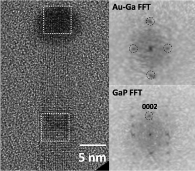 | ||
| Fig. 4 HRTEM image of a GaP NW with catalyst tip, in which the WZ structure GaP ends with a Au–Ga tip with two perpendicular lattice planes, and the FFTs are shown respectively taken from the dashed square boxes on the left side. | ||
We have noted that GaP NWs changed to a pure WZ structure with a sharp transition on the (111) plane. The lateral stacking faults in the ZB structure, plus the atomic-level transition line, all suggest that the ZB structure proceeded in a layer-by-layer growth mode on the () plane. The catalyst droplet has a low energy interface to the () ZB plane and (000) WZ plane during the whole process. This feature of a solid–liquid interface can be applied to the ZB structure growth model with different faceting. The projected side surface of <110>, <112>, and <100> ZB wires is not parallel to the growth axis. In the following text A, B, C has a meaning of labeling () planes with lateral offsets. We assume that the structures visible in the TEM images were produced during growth of the nanowires. Fig. 5a is an enlarged HRTEM image to illustrate the transition process at atomic level. In the ZB phase, the stacking sequence is illustrated as C-B-A stacking, and the side surface corresponds to a [] growth direction (Fig. 5b). A stacking fault plane, such as a B plane on top of C-B-A in the ZB phase, can result in a new B-A-B-A sequence of the WZ phase, which leads to the growth of WZ in [000] direction. In order to produce such a structure, we can assume an asymmetric nucleation at the side surface of the wire.
![Enlarged HRTEM images and 2D atomic models in the <110> viewing direction. (a) Transition from ZB to WZ, (b) the side surfaces of ZB nanowire are (111)A and (111)B planes, respectively, and atomic planes of stacking sequences during the transition are illustrated from C-B-A to B-A-B-A stacking. (c) The side surfaces of ZB NW are sawtooth-shaped with stacking units of C-B-A within dashed yellow lines, the right edges of the respective nucleus are marked by red lines. (d) Scheme of atom position at the right edge, a shift of 5{111} layers is responsible for the [001̄] direction. (e) The catalyst covers a nucleus of C-B-A layers with a lateral ledge-flow growth direction as marked with the black arrow, (f) the side surface of ZB phase corresponds to the [1̄1̄0] (55°) and [1̄1̄2̄] (71°) growth directions.](/image/article/2012/RA/c2ra21013d/c2ra21013d-f5.gif) | ||
| Fig. 5 Enlarged HRTEM images and 2D atomic models in the <110> viewing direction. (a) Transition from ZB to WZ, (b) the side surfaces of ZB nanowire are (111)A and (111)B planes, respectively, and atomic planes of stacking sequences during the transition are illustrated from C-B-A to B-A-B-A stacking. (c) The side surfaces of ZB NW are sawtooth-shaped with stacking units of C-B-A within dashed yellow lines, the right edges of the respective nucleus are marked by red lines. (d) Scheme of atom position at the right edge, a shift of 5{111} layers is responsible for the [00] direction. (e) The catalyst covers a nucleus of C-B-A layers with a lateral ledge-flow growth direction as marked with the black arrow, (f) the side surface of ZB phase corresponds to the [0] (55°) and [] (71°) growth directions. | ||
In analogy to the mechanism reported in an in situ solid catalyst growth experiment,28 growth might proceed in a ledge-flow mode from one sidewall to the other. The important difference to a layer-by-layer growth is that in this case a complete unit cell with a height of three () planes (for ZB) is nucleated and the growth front builds three layers. During the growth of the ZB phase, the nucleus at the outer edge of the Au catalyst contains a layer of the complete C-B-A stacking sequence. After nucleation the growth continues in a ledge-flow growth mechanism (as illustrated in the 2-D atomic model in Fig. 5e). We assumed for the drawing that nucleation started from the right P-rich side surface and ended at the left Ga-rich side surface. Thus, we suggest a ledge-flow growth mechanism for the GaP NWs of sub-10 nm diameter in the VLS heteroepitaxial growth on Si(111) substrate. The transition from the tilted surface of the ZB segment to the parallel surface of the WZ NW can be understood by the change of the nucleus. During the ZB NW growth, the nucleus has a more complicated C-B-A stacking with a stepped side surface. Such a nucleus requires more atoms and this results in the observed high density of stacking faults in the ZB phase. The lattice of WZ is a simple two-layer stacking sequence resulting in the [000] growth direction. In a non-equilibrium VLS NW growth, different lateral shift widths of the nucleus leads to the different growth directions that we observed. As illustrated in Fig. 5d, a lateral shift of 5 {111} planes of the nucleus results in the observed [00] growth direction. Similarly, a shift of 3 {111} planes is responsible for the [0] direction (Fig. 5f).
The photoluminescence (PL) spectra (shown in Fig. 6a) of the as-grown high-density GaP NW arrays on Si(111) substrate and the reference sample (i.e. Si NW arrays on Si(111) substrate) were measured and two PL peaks are distinguishable at about 2.4 and 2.28 eV only from the GaP NW arrays. From the Gaussian peak analysis of the PL spectra (Fig. S1†) we can find that the sample with GaP NW arrays showed the most significant light emissions at a wavelength of 539 nm (2.28 eV) with a half width of about 20 nm and at 508 nm (2.4 eV) corresponding to a smaller half width of about 10 nm, while the control measurement from Si NW arrays gave no light emission for wavelengths from 500 nm to 600 nm. Indirect energy gaps of 2.26 eV at room temperature for bulk GaP material have been reported.13 Assuming that the sub-10 nm diameter of GaP NWs changed the character of the indirect band structure towards a direct band structure, the light emission efficiency of ZB GaP would be increased. A recently published calculation predicts for WZ GaP a direct band gap at 2.25 eV, slightly smaller than the indirect band gap of ZB GaP.29 In the ZB parts of the GaP NWs a high density of structural defects such as stacking faults and twins were observed, and the surfaces of the wires were covered by native oxide. The surface defects strongly influence the physical properties of the sub-10 nm diameter NWs due to the large surface-to-volume ratio. Moreover, Si and C impurities act as shallow dopants and will introduce new energy states into the band gap. Therefore, it is possible that the PL peaks are attributed to band-to-band recombination channels caused by the impurities and defects, and a red shift would occur. The quantum confinement causes a blue shift of PL signals from small GaP particles.30 The combined effects of blue and red shifts are measured. The peak at 2.4 eV might arise from ZB GaP, the broader peak at 2.28 eV from WZ GaP.
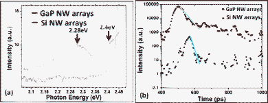 | ||
| Fig. 6 (a) PL spectra of the Au-catalyzed GaP NW arrays and Si NW arrays on Si(111) substrates at room temperature, the excitation wavelength is 475 nm. (b) Time-resolved spectra of the corresponding samples at excitation energy of 2.54 eV, the solid lines are fit to the exponential decays corresponding to 16 ps (black) and 100 ps (red), respectively. | ||
We have also measured the time-resolved properties of the two samples described above, which is an important tool for understanding how the emission changes as the electron-hole pair density changes in the NW. In the experiment, the excitation at 490 nm (2.54 eV) was superior to other ones between 450 nm to 540 nm. From Fig. 6b, we find that both Au-catalyzed GaP and Si NW arrays grown on Si(111) undergo an ultrafast light emission under our picosecond laser excitation, although the lifetimes and emission intensities are quite different. From the curve of high-density GaP NW arrays, it is apparent that, after the initial fast decay (i.e. about one order of magnitude intensity drop in less than 100 ps), a slower decay process extended to a nanosecond time scale. However, the other sample with Si NWs exhibited only fast light emission processes. The lifetime is defined as the decay time from the peak to 1/e of it. The fast decay processes fit the single exponential decays with lifetimes of 16 ps and 100 ps for Si NW arrays and GaP NW arrays, respectively. At room temperature, a high density of free carriers created by the high excitation density of laser pulse at 2.54 eV recombined non-radiatively within a short time through recombination centers on the surface. The measured decay process of Si NWs is close to the 20 ps of our time resolution. The Si decay was assumed to be much faster with a lifetime in the sub-10 ps range. Otherwise, the slower decay in the recombination of GaP NWs is attributed to the radiative lifetime of the carriers localized at impurities or defects of GaP.31 Especially, the sub-10 nm GaP NWs have a larger surface-to-volume ratio. The slower decay process can be attributed to the recombination of confined carriers in localized surface states. Besides, Au atoms were found in grown III–V NWs catalyzed by Au. 32 Au can cause unintentional doping of the NWs, or work as trap centers for recombination of electron-hole pairs. In general, the carrier lifetime of sub-10 nm GaP NW arrays was much higher than the one for Si NW arrays.
The bulk ZB phase of GaP has an indirect band gap, and for this reason only relatively weak coupling to light is expected. The crystallographic difference between ZB and WZ is mainly the number of stacked planes. For ZB three (111) planes give one unit-cell, while 2 (001) planes are required for WZ. The WZ lattice has two free parameters, which allow distortions compared to an ideal lattice based on stacking of two ZB(111) planes. Comparing the band structures of ZB and WZ phases requires calculation conditions which are as much as possible in agreement. The most important questions are the relative magnitude of direct band gap and if the gap of WZ is direct or indirect. The all-electron full-potential linearized augmented-plane wave (FP-LAPW) code ELK was used.33 It allows calculation of ab initio band structures by DFT with either LDA or GGA. Generally, band gaps calculated within this approximation are too small, thus only a comparison of relative band gaps seems to be useful. Fig. 7 shows a plot of ZB and WZ band structures, which were calculated with spin–orbit coupling and the AM05 functional.34 As expected the calculated band gap for ZB is too small. The band structure of WZ shows a smaller and direct gap. Using the value of 2.26 eV for the indirect gap of ZB and assuming a linear relation, the direct gap of WZ would be 1.87 eV. This predicted ratio is larger than the experimentally observed, which might result from different confinement effects for ZB and WZ crystals.
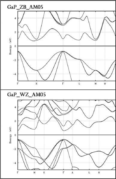 | ||
| Fig. 7 A plot of GaP ZB and WZ band structures calculated with spin–orbit coupling and the AM05 functional. | ||
Conclusions
We realized high-density sub-10 nm diameter GaP NW arrays on Si substrates, by a CBE method. Based on the analysis of the crystal structures at the base of the GaP NW and the metal catalyst tip, we concluded that, in the sub-10 nm diameter range, the growth direction of the initial ZB phase depends on the non-equilibrium multilayer ledge-flow mechanism, and WZ formation is favored by high Ga supersaturation. The combination of small radius and high supersaturation leads to formation of the relatively large nucleus with C-B-A stacking of the ZB phase. Optical characterization revealed that a band-to-band recombination occurred with an energy similar to the indirect band gap energy of bulk GaP with a short lifetime around 100 ps. The method presented here can be extended to other functionalized III–V materials integrated on Si nanostructures, and may play an important role in photoelectronic device design and the corresponding fabrication. A calculation of the WZ band gap predicts a direct band gap slightly smaller than the direct band gap of ZB. The character changes from indirect for ZB to direct for WZ.Acknowledgements
The authors would like to dedicate this paper to Ulrich Gösele, former director of the Max Planck Institute of Microstructure Physics, who passed away in November, 2009. The authors acknowledge Ms M. Herrmann for preparation of the TEM samples. We acknowledge partial support by the European NODE project 015783, the DFG project GO 704/5-1, and by the NSFC10574165.References
- X. Duan, Y. Huang, Y. Cui, J. Wang and C. M. Lieber, Nature, 2001, 409, 66 CrossRef CAS.
- Y. Cui and C. M. Lieber, Science, 2001, 291, 851 CrossRef CAS.
- M. S. Gudiksen, L. J. Lauhon, J. Wang, D. C. Smith and C. M. Lieber, Nature, 2002, 415, 617 CrossRef CAS.
- G. Kästner, U. Gösele and T. Y. Tan, Appl. Phys. A: Mater. Sci. Process., 1998, 66, 13 CrossRef.
- T. Martensson, C. P. Svensson, B. A. Wacaser, M. W. Larsson, W. Seifert, K. Deppert, A. Gustafsson, L. R. Wallenberg and L. Samuelson, Nano Lett., 2004, 4, 1987 CrossRef CAS.
- E. P. A. M. Bakkers, M. Borgstrom and M. Verheijen, MRS Bull., 2007, 32, 117 CrossRef CAS.
- R. S. Wagner and W. C. Ellis, Vapor-Liquid-Solid Mechanism of Single Crystal Growth, Appl. Phys. Lett., 1964, 4, 89 CrossRef CAS.
- E. I. Givargizov, J. Cryst. Growth, 1975, 31, 20 CrossRef CAS.
- H. J. Joyce, Q. Gao, H. H. Tan, C. Jagadish, Y. Kim, X. Zhang, Y. Guo and J. Zou, Nano Lett., 2007, 7, 921 CrossRef CAS.
- A. Lugstein, A. M. Andrews, M. Steinmair, Y. Hyun, E. Bertagnolli, M. Weil, P. Pongratz, M. Schramböck, T. Roch and G. Strasser, Nanotechnology, 2007, 18, 355306 CrossRef.
- W. Seifert, M. Borgström, K. Deppert, K. A. Dick, J. Johansson, M. W. Larsson, T. Martensson, N. Sköld, P. T. Svensson, B. A. Wacaser, L. R. Wallenberg and L. Samuelson, J. Cryst. Growth, 2004, 272, 211 CrossRef CAS.
- A. L. Roest, M. A. Verheijen, O. Wunnicke, S. Serafin, H. Wondergem and E. P. A. M. Bakkers, Nanotechnology, 2006, 17, S271 CrossRef CAS.
- M. R. Lorenz, G. D. Pettit and R. C. Taylor, Phys. Rev., 1968, 171, 876 CrossRef CAS.
- Z. Zhang, T. Shimizu, L. Chen, S. Senz and U. Gösele, Adv. Mater., 2009, 21, 2824 CrossRef CAS.
- Z. Huang, X. Zhang, M. Reiche, L. Liu, W. Lee, T. Shimizu, S. Senz and U. Gösele, Nano Lett., 2008, 8, 3046 CrossRef CAS.
- R. E. Algra, M. A. Verheijen, M. T. Borgström, L. Feiner, G. Immink, W. J. P. van Enckevort, E. Vlieg and E. P. A. M. Bakkers, Nature, 2008, 456, 369 CrossRef CAS.
- U. Krishnamachari, M. Borgstrom, B. J. Ohlsson, N. Panev, L. Samelson, W. Seifert, M. W. Larsson and L. R. Wallenberg, Appl. Phys. Lett., 2004, 85, 2077 CrossRef CAS.
- M. T. Borgström, G. Immink, B. Ketelaars, R. Algra and E. P. A. M. Bakkers, Nat. Nanotechnol., 2007, 2, 541 CrossRef.
- K. Tomioka, J. Motohisa, S. Hara and T. Fukui, Nano Lett., 2008, 8, 3475 CrossRef CAS.
- G. M. Kuznetsov and Y. I. Shmelev, Inorg. Mater. USSR, 1974, 10, 1078 Search PubMed.
- V. Schmidt, S. Senz and U. Gösele, Nano Lett., 2005, 5, 931 CrossRef CAS.
- T. Akiyama, K. Sano, K. Nakamura and T. Ito, Jpn. J. Appl. Phys., 2006, 45, L275 CrossRef CAS.
- F. Glas, J.-C. Harmand and G. Patriarche, Phys. Rev. Lett., 2007, 99, 146101 CrossRef.
- H. Shtrikman, R. Popovitz-Biro, A. Kretinin, L. Houben, M. Heiblum, M. Bukala, M. Galicka, R. Buczko and P. Kacman, Nano Lett., 2009, 9, 1506 CrossRef CAS.
- Binary Alloy Phase Diagrams, ed. T. B. Massalski, et al., ASM international, Materials Park, Ohio, 2nd edn, 1998, vol. 1 Search PubMed.
- B. J. Kim, J. Tersoff, C.-Y. Wen, M. C. Reuter, E. A. Stach and F. M. Ross, Phys. Rev. Lett., 2009, 103, 155701 CrossRef CAS.
- V. K. Dixit, T. Ganguli, T. K. Sharma, S. D. Singh, R. Kumar, S. Porwal, P. Tiwari, A. Ingale and S. M. Oak, J. Cryst. Growth, 2008, 310, 3428 CrossRef CAS.
- S. Hofmann, R. Sharma, C. T. Wirth, F. Cervantes-Sodi, C. Ducati, T. Kasama, R. E. Dunin-Borkowski, J. Drucker, P. Bennett and J. Robertson, Nat. Mater., 2008, 7, 372 CrossRef CAS.
- A. De and C. E. Pryor, Phys. Rev. B: Condens. Matter Mater. Phys., 2010, 81, 155210 CrossRef.
- Y.-H. Kim, Y. Jun, B.-H. Jun, S.-M. Lee and J. Cheon, J. Am. Chem. Soc., 2002, 124, 13656 CrossRef CAS.
- C. A. Dimitriadis, Solid-State Electron., 1983, 26, 633 CrossRef CAS.
- D. E. Perea, J. E. Allen, S. J. May, B. W. Wessels, D. N. Seidman and L. J. Lauhon, Nano Lett., 2006, 6, 181 CrossRef CAS.
- http://elk.sourceforge.net .
- R. Armiento and A.E. Mattson, Phys. Rev. B: Condens. Matter Mater. Phys., 2005, 72, 085108 CrossRef.
Footnote |
| † Electronic Supplementary Information (ESI) available: details of fabrication of GaP & Si nanowire arrays, experimental instruments, identification of Au–Ga phases, the Gaussian peak fit of PL spectra of GaP NW arrays, and the parameters used in calculations of ab initio band structures. See DOI: 10.1039/c2ra21013d |
| This journal is © The Royal Society of Chemistry 2012 |