Controlled performance of an organic transistor memory device with an ultrathin LiF blocking layer
Sumei
Wang
*abd,
Paddy K. L.
Chan
*b,
Chi
Wah Leung
c and
Xurong
Zhao
ad
aKey Laboratory for Liquid-Solid Structural Evolution and Processing of Materials, Shandong University, Jinan, 250061, P. R. China
bDepartment of Mechanical Engineering, The Hong Kong Polytechnic University, Kowloon, Hong Kong. E-mail: pklc@hku.hk
cDepartment of Applied Physics, The Hong Kong Polytechnic University, Kowloon, Hong Kong
dEngineering Ceramics Key Laboratory of Shandong Province, Shandong University, Jinan, 250061, P. R. China. E-mail: wangsumei3000@sdu.edu.cn (Sumei Wang)
First published on 2nd August 2012
Abstract
In this paper, the controlled performance of a novel organic pentacene transistor memory device with an ultrathin LiF blocking layer was investigated. Our results demonstrate the introduction of an ultrathin LiF layer has a significant influence on the transistor memory performance. As the LiF thickness increased from 0 to 3 nm, the charge carrier mobility showed a three-fold increase from 0.15 to 0.43 cm2 V−1 s−1 due to hole injection enhancement. Moreover, the on/off current ratio increased from 5 to 50 at long measurement times. This significant enhancement of charge retention behavior (∼10 times improvement) was ascribed to the LiF blocking effect when the trapped charge was released from silver nanoparticle induced trap centers. However, the memory window showed a slight decrease from 60 to 37 V, which is due to the decreased penetration depth of silver nanoparticles into the pentacene layer. The physical origin of the memory effect with the LiF ultrathin layer was also discussed. Our introduction of an ultrathin LiF layer offers a simple and feasible way to control the different memory performances of this novel transistor memory device.
Introduction
Organic electronic devices have attracted considerable attention owing to their low cost, large area processing and potential application on flexible substrates.1 Significant progress in device structure and materials have been achieved in recent years, including organic light-emitting diodes (OLEDs),2,3 organic field-effect transistors (OFETs)4 and organic solar cells,5,6 allowing the organic devices to have a high chance for commercialization. Among the various types of organic electronics, organic nonvolatile memory (ONVM) plays an important role in data storage as well as memory buffering. Organic flash memories fabricated on flexible substrates have great application potential for integration with other flexible electronic devices and provide the data storage capacity in organic chips. To achieve organic memory devices with performances comparable with inorganic memory, there are three key areas of scaling challenges:7 (1) physical dimension scaling, which mainly depends on the lithograph technology and the cell layout design; (2) electrical scaling, which aims to reduce the operating power and lower the write/erase/read voltage of the memory device; (3) reliability and retention time scaling. For stable storage, it is important for the memory devices to have a long retention time, fast operating speed, large carrier mobility and short writing/erasing time.Among different configurations of organic memory devices, OFET-based memory is considered the most promising candidate because of its nondestructive read-out, complementary integrated circuit architectural compatibility, and single transistor realization.8 A floating gate transistor memory device is a modified MOS transistor that introduces an additional electrically isolated gate (named floating gate) as the charge storage component. Adding or removing charges from the floating gate changes the threshold voltage of the cell, thereby defining the memory state of the cell. The design of the tunneling dielectric and charge trapping layers are important as they directly affect the write or read speed and non-volatility of the memory cell.9–11
In nonvolatile memory devices, data retention refers to the ability of a memory bit (stored charge) to be retained over long periods of time, and a long retention time is necessary for high performance memory devices. In inorganic Si-based nonvolatile memory devices, the retention time can reach 10 years for flash memory with NOR device architecture.12 In comparison, the retention time of organic flash memory devices is usually around several hours to a few days.13,14 For example, an organic flash memory array with a floating gate embedded in hybrid dielectrics comprising a 2 nm molecular self-assembled monolayer (SAM) and a 4 nm Al2O3 layer on a flexible substrate has been reported;15 however, the retention time was around one day. Therefore, long memory retention behavior is still a big challenge in organic nonvolatile memory devices, and it should be overcome for realistic application in integrated circuits.
Different approaches have been applied for improving the charge retention property of the devices. One approach is to introduce discontinuous nanoparticles or nanocrystals instead of continuous films as the floating gate charge trapping layer; this minimizes the charge loss and hence reduces the current leakage, similar to the silicon based nonvolatile memory device.16,17 Another approach is to introduce a thin insulating blocking layer between the ferroelectric dielectric layer and the semiconductor active layer in ferroelectric transistor memory devices.18 Due to the blocking effect of the inserted insulating layer, the rate of charge releasing process from trap centers can be lowered, thus the charge retention property can be improved to a certain extent. The side-effect of this approach in ferroelectric transistor memory devices is that the insulating layer easily forms the depolarization field and thus weakens the ferroelectric polarization field.18,19
Recently, we reported a novel floating nanoparticle transistor memory device with a significantly large memory effect by embedding silver nanoparticles in between two pentacene layers.20,21 A remarkable advantage of this memory is high carrier mobility and the simplicity of the fabrication procedure, which is suitable for integrating with other electronic devices on the same substrate. In this contribution, we introduce an ultrathin LiF layer underneath the Ag nanoparticles as the charge blocking layer in this novel organic memory device. To the best of our knowledge, a LiF layer is rarely used in organic memory devices, despite its wide use in OLED devices as an effective electron injection layer. Our experimental results showed that a 3 nm thick LiF layer can effectively block the incoming Ag atoms during deposition and prevent them from penetrating into the bottom layer of pentacene. The obtained memory devices have high performance, such as long retention time, a high on/off current ratio, and a high memory window. These performance enhancements make the current organic memory more suitable for potential applications in integrated circuits.
Experimental
Device fabrication
The bottom-gate transistor memory devices were fabricated on highly-doped n-type Si substrates with 300 nm SiO2, and from bottom to top, the device configuration was in the form of pentacene–LiF–Ag nanoparticles–pentacene. Si Substrates were cleaned by sonication in DI water, acetone, and isopropanol. After cleaning, the substrates were exposed to UV ozone plasma for 15 min and then functionalized with a self-assembled monolayer of octadecyltrichlorosilane (OTS) by immersing the substrate in a OTS–hexane solution (1![[thin space (1/6-em)]](https://www.rsc.org/images/entities/char_2009.gif) :500 v/v%). Pentacene films, a thin LiF layer and a Ag nanoparticle layer were thermally evaporated at a base pressure of 1 × 10⁻⁷ Torr in one pumpdown. The thickness of the bottom and top pentacene layers were 15 nm and 25 nm respectively. The deposition rates of the pentacene, LiF and Ag nanoparticle layers were 0.5, 0.2 and 0.1 A s−1, respectively. The thickness of the LiF layer was about 1 nm (device A1) and 3 nm (device A3). For comparison, a device without a LiF layer was also fabricated (device A0). To eliminate the effect of the LiF layer on the memory performance of the memory device, we also fabricated a comparison device (device A4) with 3 nm LiF between two pentacene layers without Ag nanoparticles. Top contact transistor memory device was completed by the deposition of 50 nm thick silver source and drain electrodes by a shadow mask. The obtained device has channel lengths and widths of 50 μm and 1000 μm, respectively.
:500 v/v%). Pentacene films, a thin LiF layer and a Ag nanoparticle layer were thermally evaporated at a base pressure of 1 × 10⁻⁷ Torr in one pumpdown. The thickness of the bottom and top pentacene layers were 15 nm and 25 nm respectively. The deposition rates of the pentacene, LiF and Ag nanoparticle layers were 0.5, 0.2 and 0.1 A s−1, respectively. The thickness of the LiF layer was about 1 nm (device A1) and 3 nm (device A3). For comparison, a device without a LiF layer was also fabricated (device A0). To eliminate the effect of the LiF layer on the memory performance of the memory device, we also fabricated a comparison device (device A4) with 3 nm LiF between two pentacene layers without Ag nanoparticles. Top contact transistor memory device was completed by the deposition of 50 nm thick silver source and drain electrodes by a shadow mask. The obtained device has channel lengths and widths of 50 μm and 1000 μm, respectively.
Characterization
The surface morphology was characterized by nanoscope tapping mode atomic force microscopy. X-ray photoelectron spectroscopy was recorded to characterize the Ag depth profile in the memory device. Monochromated Al Kα (1486.6 eV) X-rays were used and coronene ions as the sputtering source with an X-ray beam diameter of 100 μm. The current–voltage characteristics of the transistor memory devices were measured using two Keithley 2400 sourcemeters connected to the computer. All the measurements were performed in dark and ambient conditions immediately after the devices were fabricated.Results and discussion
In the current transistor memory device, the Ag nanoparticles worked as the charge storge layer and the LiF acted as the charge blocking layer, which had a significant influence on the memory performance. Therefore, we first investigated the atomic force microscopy (AFM) surface morphology of the Ag nanoparticles and LiF layer on the bottom pentacene layer, as shown in Fig. 1 (a–c). The samples are: (a) 1 nm Ag–15 nm pentacene, (b) 1 nm Ag–1 nm LiF–15 nm pentacene, (c) 1 nm Ag–3 nm LiF–15 nm pentacene, the substrates for these three samples are 300 nm SiO2–Si substrate. When 1 nm Ag was deposited on a 15 nm pentacene layer without a LiF layer, the grain boundary of the deposited pentacene can be seen clearly. However, when 1 nm LiF was introduced between Ag NPs and the bottom pentacene layer, some small nanoparticles were randomly distributed in clusters on the pentacene layer, indicating that 1 nm LiF can effectively block Ag penetration into the pentacene layer. Further, when the thickness of the LiF layer increased to 3 nm, the number of very small clusters increased greatly, and these very small clusters become almost continuous. In addition, the grain boundaries of pentacene became obscure due to the screening effect of the LiF layer. It should be noted that these clusters should be the combination of Ag nanoparticles and LiF clusters, as 1 nm Ag could not fully cover the underneath layer.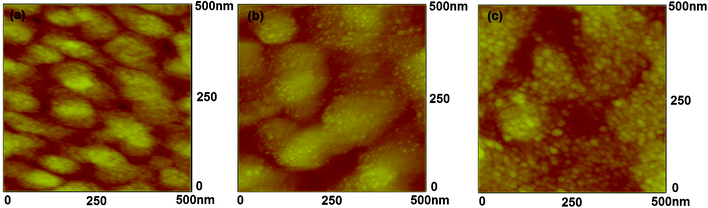 | ||
| Fig. 1 The AFM surface morphology for Ag nanoparticles and LiF on the bottom pentacene layer (a) 1 nm Ag–15 nm pentacene, (b) 1 nm Ag–1 nm LiF–15 nm pentacene, (c) 1 nm Ag–/3 nm LiF–15 nm pentacene, the substrates for these three samples are 300 nm SiO2–Si substrate. | ||
In order to check the penetration depth of Ag into the pentacene layer, XPS depth profile measurements were performed for the samples shown in Fig. 2 (a–d) (a) 1 nm Ag–15 nm pentacene, (b) 1 nm Ag–/1 nm LiF–15 nm pentacene and (c) 1 nm Ag–3 nm LiF–15 nm pentacene, all deposited on 300 nm SiO2–Si substrates. Fig. 2 (d) is the comparison for Ag atom depth profile in these three samples. Silver and carbon are present in significant quantities on the surface of these three samples. The presence of carbon comes from the pentacene layer due to the exposed pentacene surface not covered by Ag nanoparticles and LiF, as shown in the AFM images. The fluorine atoms detected in samples (b) and (c) originate from the LiF layer. With increasing etch depth, the silver atom concentration decreases due to the reduced penetration ability and the increasing signal contribution from silicon and oxygen. At an etching time of about 2500 s, the atomic concentration of silicon, oxygen and carbon are stabilized and this is assumed to be the SiO2 layer (as shown in the dotted line of Fig. 2 (a–c)). By knowing the total layer thickness and the etching time, one can convert the etching depth at every etching time and the Ag depths can be calculated to be 5.1 nm, 3.6 nm and 3.4 nm respectively for samples (a) to (c). These results indicate that with the introduced LiF layer, the penetration depth of the Ag atom was decreased, which may have a significant influence on the memory device performance.
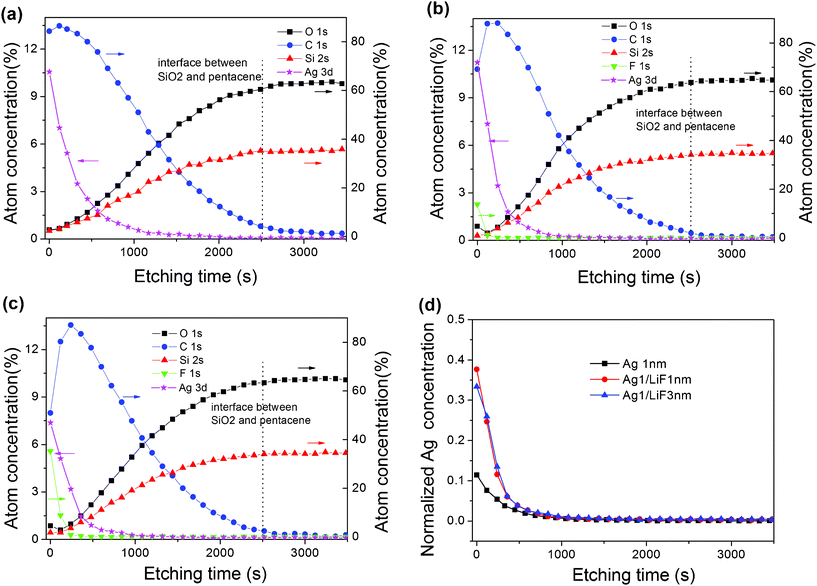 | ||
| Fig. 2 The XPS depth profile result for Ag nanoparticles and LiF on the bottom pentacene layer (a) 1 nm Ag–15 nm pentacene, (b) 1 nm Ag–1 nm LiF–15 nm pentacene, (c) 1 nm Ag–3 nm LiF–15 nm pentacene, the substrates for these three samples are 300 nm SiO2–Si substrate; (d) comparison for Ag atom depth profile in these three samples. | ||
The electrical output characteristics of devices A0, A1 and A3 are shown in Fig. 3 (a–c). The gate voltage (Vg) was varied from 0 to −60 V with a 10 V step. The output curves exhibit a typical p-channel field-effect transistor behavior with the hole accumulation mode at negative Vg and hole depletion mode at positive Vg. The drain-source current in the saturation region increases from 9 μA in device A0 to 60 μA in device A3. As listed in Table 1, the field-effect mobility (μ) in the saturation region is calculated to be 0.15 cm2 V−1 s−1 for device A0, and it increases to 0.43 cm2 V−1 s−1 for device A3. The increases in carrier mobility and saturation current with the increase of LiF thickness is attributed to the improvement of hole injection. It seems that the high built in field formation due to a large dielectric constant of LiF (ε = 9.1) is responsible for the better charge injection and memory performance.22,23 On the other hand, for the device A0 without LiF, as shown in Fig. 3(a), the drain-source current decreases at large drain-source voltage, which is related to the existing charge trap states in the channel caused by the deposition of the Ag nanoparticles layer or Ag electrode and diffusion into organic semiconductor layer.24,25 For device A0 without an LiF layer, as shown in the XPS profile data, the Ag nanoparticles can penetrate with a higher depth, and some Ag nanoparticles may diffuse into the pentacene channel and work as charge traps. The schematic demonstrations of the charge transport process are shown in Fig. 4. After applying a certain gate voltage, at the first stage, when the drain-source voltage Vds is small, these traps state are empty so the drain-source current increases with the increased Vds. However, once the traps are filled, the screening effect of these traps states will lead to a decrease of the drain-source current. Therefore, a decreased drain-source current, instead of saturated current, was obtained at large drain source voltage. On the contrary, for the devices with an LiF layer, there is nearly no Ag nanoparticle induced charge traps in the pentacene channel position, therefore good saturation curves were obtained at large drain-source voltages. This phenomenon indicates the excellent blocking effect of the LiF layer in this memory device.
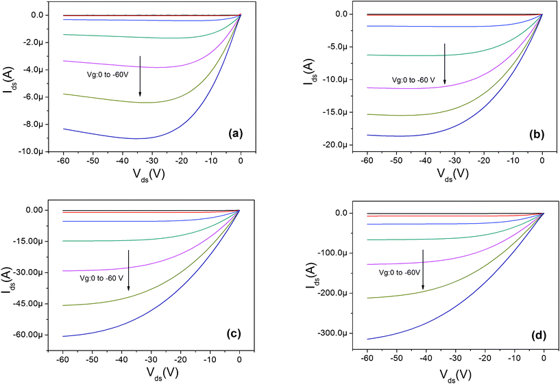 | ||
| Fig. 3 The output characteristics for transistor memory device: (a) A0: Ag nanoparticles 1 nm without LiF, (b) A1: 1 nm LiF and 1 nm Ag nanoparticles, (c) A3: 3 nm LiF and 1 nm Ag nanoparticles, and (d) A4: 3 nm LiF without Ag nanoparticles. | ||
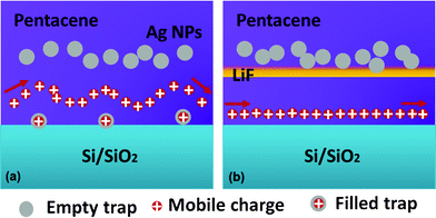 | ||
| Fig. 4 Schematic demonstration of the charge transport mechanism: (a) the screening effect caused by Ag nanoparticle traps states in the device channel without an LiF layer; (b) the LiF blocking effect for Ag nanoparticle penetration into the pentacene channel in the device with an LiF layer. | ||
| Devices | Mobility (cm2 V−1 s−1) | ΔVth (V) | On/off ratio |
|---|---|---|---|
| A0 (Ag 1 nm without LiF) | 0.15 | 60 | 104–105 |
| A1 (LiF 1–Ag 1) | 0.22 | 56 | 104 |
| A3 (LiF 3–Ag 1) | 0.43 | 37 | 104 |
| A4 (LiF 3 nm without Ag nanoparticles) | 0.72 | 8 | 105–106 |
The hysteretic memory properties of the devices were investigated by cyclic sweeping of Vg (i.e. from positive to negative and then back to positive). The memory window of a device is defined as the change of the threshold voltages in these two gate voltage sweeping directions, i.e. ΔVth = Vth1 − Vth2. As shown in Fig. 5 (a), the memory window shows a remarkable dependence on the thickness of the LiF layer. For device A0 without an LiF layer, the memory window is about 60 V, with a large on/off current ratio of 104–105. However, the memory window decreases with the increasing thickness of the LiF layer. The memory window of device A1 with 1 nm LiF is about 56 V; it decreases to 37 V for device A3 with 3 nm LiF. The memory window ΔVth is related to the charge traps density Δn with the following relationship:26
 | (1) |
 | ||
| Fig. 5 The memory effects for the device with and without a LiF layer. (a) Memory window and (b) charge retention behavior. | ||
To eliminate the effect of the LiF layer on the memory effect, we also investigated device A4 with only a 3 nm LiF layer but no Ag nanoparticle layer, as shown in Fig. 3 (d) and Fig. 4 (a). For this kind of device, the saturation drain current and the charge carrier mobility are 300 μA and 0.72 cm2 V−1 s−1 respectively, much higher than device A3 with 3 nm LiF and 1 nm Ag NPs. The hysteresis effect of A4 is only 8 V, much lower than that of device A3 (37 V). This small hysteresis indicates that the LiF layer itself cannot induce enough trap density for the memory device, which proves that the memory effect in the device with an LiF layer and Ag nanoparticles is mainly due to the trap states induced by Ag nanoparticles. Comparing device A3 (3 nm LiF and 1 nm Ag NPs) and A4 (3 nm LiF without Ag NPs), it can be found that the increased off current in device A3 maybe related to the conductive current path caused by Ag nanoparticles.
The memory hysteresis mechanism in this novel memory device is shown in the schematic diagrams in Fig. 5. The Ag nanoparticles sandwiched by two pentacene layers act as the charge trapping elements of the holes. When the positive gate voltage is applied, holes are injected from the bottom pentacene layer to the Ag nanoparticles and are trapped in the Ag nanoparticles. Therefore, the trapped holes form a built-in electric field E1 opposite to the applied external electric field, as shown in Fig. 5 (c), which assists channel formation and result in a positive Vth shift when the gate bias sweeps from the positive to the negative direction. On the contrary, when the negative gate bias is applied, a charge detrapping process will take place either by direct hole injection from Ag nanoparticles to the pentacene layer or by recombination with the negative charges, resulting in a negative Vth shift. Therefore, this kind of OFET can be utilized in organic nonvolatile memory devices.
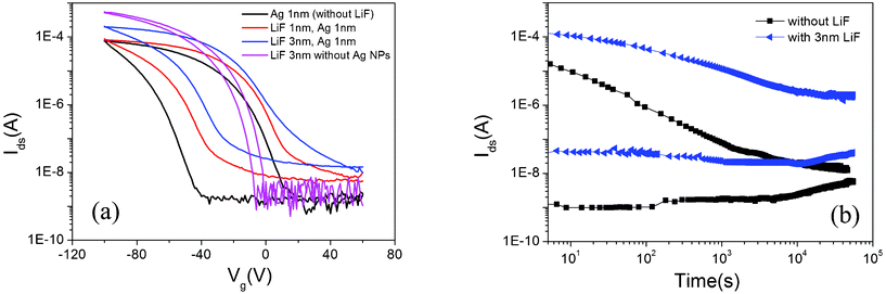
The retention time of charge carriers is another important parameter for assessing the performance of nonvolatile memory devices. Fig. 5 (b) shows the retention time of on- and off-currents for the memory device with and without an LiF layer. After applying a writing pulse of +100 V (erasing pulse of −100 V) with a pulse width of 15 s, we measured the on- (off-) current with time intervals of 60 s at Vg = 0 V and Vds = −60 V. As shown in Fig. 5 (b), for the device without LiF, the off-current increases slightly but the on-current decays in a fast rate. As a result, the initial on/off current ratio of 104 decreased dramatically to around 5 after 15 h. On the contrary, for the memory device with 3 nm LiF, the on current decays at a lower rate than that without an LiF layer. Therefore, the on/off ratio still remained at about 50 after 15 h and then the ratio became stable. This 10 times improvement of on/off current ratio indicated that the memory retention behavior can be remarkably improved by introducing the LiF layer. A similar effect of a 4 nm Al2O3 layer as a buffer layer has also been reported for the amorphous indium–gallium–zinc oxide based ferroelectric transistor memory device with improved charge retention behavior; however, the improved on/off current ratio of 70 is just within the retention measurement time of 10000 s, and it is shorter than that in our work.18
Conclusions
An organic nonvolatile transistor memory with floating Ag nanoparticles and an LiF charge blocking layer is studied by comparing the memory window, mobility and charge retention properties. When the LiF thickness increased from 0 to 3 nm, the silver nanoparticle penetration depth varied from 5 nm to 3 nm, and the memory window decreased from 60 V to 37 V. Other than the memory window, the charge carrier mobility was improved greatly from 0.15 to 0.43 cm2 V−1 s−1 due to the hole injection enhancement. Moreover, the retention behavior was dramatically enhanced by inserting a 3 nm LiF layer between the bottom pentacene and Ag nanoparticles, with an increase in the on/off current ratio from 5 to 50 at a measurement time of 15 h. The great enhancement of the charge retention behavior by the LiF blocking effect opens a new direction in designing the structure of organic memory devices.Acknowledgements
This work was supported by the National Natural Science Fountain of China (No. 61106086), the promotive research fund for excellent young and middle-aged scientists of Shandong Province (BS2011DX014) and the Independent Innovation Foundation of Shandong University (IIFSDU, No. 2011TB016).References
- H. Sirringhaus, Adv. Mater., 2009, 21, 3859 CrossRef CAS.
- S. C. Lo and P. L. Burn, Chem. Rev., 2007, 107, 1097 CrossRef CAS.
- S. R. Forrest and M. E. Thompson, Chem. Rev., 2007, 107, 923 CrossRef CAS.
- R. P. Ortiz, A. Facchetti and T. J. Marks, Chem. Rev., 2010, 110, 205 CrossRef CAS.
- B. C. Thompson and Jean M. J. Frechet, Angew. Chem., Int. Ed., 2008, 47, 58 CrossRef CAS.
- S. Gunes, H. Neugebauer and N. S. Sariciftci, Chem. Rev., 2007, 107, 1324 CrossRef.
- S. K. Lai, IBM J. Res. Dev., 2008, 52, 529 CrossRef.
- K. J. Baeg, Y. Y. Noh, H. Sirringhaus and D. Y. Kim, Adv. Funct. Mater., 2010, 20, 224 CrossRef CAS.
- D. Gupta, M. Anand, S. W. Ryu, Y. K. Choi and S. H. Yoo, Appl. Phys. Lett., 2008, 93, 224106 CrossRef.
- J. S. Lee, J. H. Cho, C. Y. Lee, I. Kim, J. J. Park, Y.-M. Kim, H. Y. Shin, J. Lee and F. Caruso, Nat. Nanotechnol., 2007, 2, 790 CrossRef CAS.
- K. Galatsis, K. Wang, Y. Botros, Y. Yang, Y. H. Xie and J. F. Stoddart, IEEE Circuits Devices Mag., 2006, 22, 12 CrossRef.
- W. L. Leong, P. S. Lee, A. Lohani, Y. M. Lam, T. P. Chen, S. Zhang, A. Dodabalapur and S. G. Mhaisalkar, Adv. Mater., 2008, 20, 2325 CrossRef CAS.
- K. H. Lee, G. Lee, K. Lee, M. S. Oh and S. Im, Appl. Phys. Lett., 2009, 94, 093304 CrossRef.
- K. J. Baeg, Y. Y. Noh, J. Ghim, B. Lim and D. Y. Kim, Adv. Funct. Mater., 2008, 18, 3678 CrossRef CAS.
- T. Sekitani, T. Yokota, U. Zschieschang, H. Klauk, S. Bauser, K. Takeuchi, M. Takamiya, T. Sakurai and T. Someya, Science, 2009, 326, 1516 CrossRef CAS.
- Q. Winkler, M. Baus, M. C. Lemme, R. Rolver, B. Spangenberg and H. Kurz, Materials for information technology: devices, interconnects and packaging, Springer, 2005, pp. 127–138 Search PubMed.
- M. H. White, Y. Yang, A. Purwar and M. L. French, IEEE Trans. Compon., Packag., Manuf. Technol., Part A, 1997, 20, 190 CrossRef CAS.
- S. M. Yoon, S. H. Yang, S. W. Jung, C. W. Byun, S. H. Park, C. S. Hwang, G. G. Lee and H. Ishiwara, Appl. Phys. Lett., 2010, 96, 232903 CrossRef.
- S. M. Yoon, S. Yang, S. H. Ko Park, S. W. Jung, C. W. Byun, D. H. Cho, S. Y. Kang, C. S. Hwang and B. G. Yu, J. Phys. D: Appl. Phys., 2009, 42, 245101 CrossRef.
- S. M. Wang, C. W. Leung and P. K. L. Chan, Org. Electron., 2010, 11, 990 CrossRef CAS.
- S. M. Wang, C. W. Leung and P. K. L. Chan, Appl. Phys. Lett., 2010, 97, 023511 CrossRef.
- T. Oyamada, H. Tanaka, K. Matsushige, H. Sasabe and C. Adachi, Appl. Phys. Lett., 2003, 83, 1252 CrossRef CAS.
- T. L. Choi, K. H. Lee, S. K. Lee, T. W. Lee and M. Y. Chae, J. Am. Chem. Soc., 2007, 129, 9842 CrossRef CAS.
- L. Z. Yu and C. T. Lee, Appl. Phys. Lett., 2009, 95, 103305 CrossRef.
- J. S. Chen, L. L. Xu, J. Lin, Y. H. Geng, L. X. Wang and D. G. Ma, Appl. Phys. Lett., 2006, 89, 083514 CrossRef.
- K. Baeg, Y. Noh, J. Ghim, S. Kang, H. Lee and D. Kim, Adv. Mater., 2006, 18, 3179 CrossRef CAS.
| This journal is © The Royal Society of Chemistry 2012 |