In situ growth of Au nanoparticles on the surfaces of Cu2O nanocubes for chemical sensors with enhanced performance†
Xiao-Wang
Liu
*,
Feng-Yun
Wang
,
Fang
Zhen
and
Jia-Rui
Huang
*
College of Chemistry and Materials Science, Anhui Key Laboratory of Functional Molecular Solids, Anhui Normal University, Anhui Key Laboratory of Molecule-based Materials, Wuhu, 241000, P. R. China. E-mail: xwliu601@mail.ahnu.edu.cn; jrhuang@mail.ahnu.edu.cn; Fax: +86 05533869302; Tel: +86 05533869302
First published on 4th July 2012
Abstract
An in situ strategy has been developed to directly grow Au nanoparticles (NPs) on the surfaces of Cu2O nanocubes by exposing Cu2O nanocubes to diluted HAuCl4 solution at room temperature. The sensing performances of the Cu2O nanocubes toward ethanol and acetone improved significantly after the growth of the Au NPs.
Fabrication of nanostructure-based gas sensors with high sensitivity, selectivity, stability and improved response and recovery time is one of the most important branches of nanotechnology.1,2 The bottom-up approach, a commonly used strategy to synthesize nanomaterials, offers us a powerful tool to control the physical properties of the products, such as size, shape and composition, subsequently allowing for the development of low-cost, fast-response and sensitive gas sensors.3–5 In most cases, metal oxides, which have a receptor and transducer function, are used as gas-sensing materials as their electrical resistances will change correspondingly upon exposure to oxidizing or reducing gases. In the sensing process, specific interaction between a metal oxide surface and target molecules is required and the materials should have further ability to transfer the interaction-induced-alterations from the surfaces into a macroscopically accessible signal, typically, a change in the electrical resistance. In principle, engineering sensing materials’ structures can enhance the properties of gas sensors, such as increasing the sensitivity and generating a faster response and recovery time.6–8 As a result, highly porous and hollow structures have been synthesized via various methods in order to improve gas diffusion and mass transport in the sensing process.9–12 Another potential way to improve sensor performance is to enhance the catalytic activity as their conductivity response is determined by the catalytic efficiency of the reactions between detected gas molecules and gas-sensing materials taking place on the surfaces.13 Noble metal NPs, such as Au, Ag, Pt and Pd, are highly-effective oxidation catalysts that make them of use as active materials to improve the reactions occurring on gas-sensor surfaces.14–17 Thus, various techniques, including impregnation, sol–gel, sputtering and thermal evaporation, have been exploited for introducing noble metal additives onto/into oxide semiconductors. After the functionalization, different gas sensors with improved behaviors were obtained.
Cu2O, a p-type semiconductor with a direct band gap of about 2.17 eV, has emerged as a star material in recent years owing to its distinguished properties and great potential in gas sensing,18–21 catalysis,22 solar energy conversion,23 biosensing,24 and electrode materials.25 The possibility of using Cu2O nanostructures as gas-sensor materials has been demonstrated,18–21 but in principle pure Cu2O is not an ideal gas-sensing material in terms of its physical characteristics. On one hand, the operating mechanism for a transition-metal-oxide is based on the change in resistance which is determined by the mobility of charge carriers. The mobility of positive holes in p-type metal oxides is usually much lower than that of conduction electrons in n-type semiconductors, for example, the mobility of Cu2O is about 10 cm2 V−1 s,26 while the mobilities are about 160 and 200 cm2 V−1 s for SnO2 and ZnO, respectively. On the other hand, regardless of p-type or n-type semiconductor sensor, ionosorption of oxygen and the formation of negatively charged ions, such as O−, O2− and O2−, are necessary pre-procedures in gas sensing. Obviously, the quantity of absorbed oxygen anions plays a vital role in determining the performance of a sensor as they will directly react with target analyte, releasing electrons back to the conduction band and leading to a significant decrease in resistance for n-type semiconductors and a sharp increase in resistance for p-type gas-sensing materials. For n-type semiconductors, electron conduction is dominant, that is, plenty of electrons are available for ionization of absorbed oxygen; however, for p-type semiconductors, positive holes are the major charge carriers and the surface concentrations of electrons are much lower than those in n-type oxides.27 As a result, less attention has been paid to the fabrication of gas sensors based on p-type metal oxides. However, if other advantages of n-type oxides such as low cost and non-toxicity are taken into account, the sophisticated design and synthesis of n-type oxide nanostructures or n-type oxide-based nanocomposites for gas sensors with improved sensing performance is still of great interest. Herein, we report a facile in situ method for the homogeneous growth of Au NPs on the surfaces of Cu2O nanocubes by exposing Cu2O nanocubes to diluted chloroauric acid directly. In comparison with sputtering, impregnation and other surface modification techniques, in situ growth methods have exhibited several features in the uniform loading of Au NPs: (1) avoiding introduction of impurities as no extra reducing agents or surfactants are required; (2) operations are performed under mild conditions.28,29 Gas-sensing studies indicate that the sensitivity of Cu2O nanocubes toward ethanol and acetone is significantly improved after the decoration of Au NPs. This enhanced performance may derive from deeper, continuous electron-depleted layers formed on the surfaces of Cu2O nanocubes. These layers may be caused by the homogeneous distribution of Au NPs and small size of the Cu2O nanocubes.16
Cu2O nanostructures were first synthesized by a surfactant-free method (ESI†). TEM measurements (Fig. 1a) show that the as-prepared nanostructures have cubic morphology with an average width of about 45 nm, and the edges of the nanocubes are clear and smooth. The light yellow colloid solution gradually changed to black, forming CuO nanostructures at room temperature when the products were dispersed in distilled water under the atmosphere, indicating that the as-prepared Cu2O nanocubes have quite a strong reducing capacity as they can be easily oxidized by oxygen. The reduction capacity of the Cu2O nanocubes may be employed to reduce noble metal ions without the assistance of additional reductive reagents; the freshly produced noble metal atoms might deposit on the surfaces of the Cu2O nanocubes and act as seeds to further grow NPs in order to reduce surface energy in the reaction system. As a result, Cu2O–metal nanocomposites may be produced. As expected, when a Cu2O nanocube colloid solution was injected into HAuCl4 at room temperature, the color of the mixture changed from light yellow to black immediately. Fig. 1b shows a typical TEM image of Cu2O nanocubes after incubation with Au precursor for 5 s. It is clear that a great number of NPs with diameters of about 5 nm were homogeneously formed on the surfaces of Cu2O nanocubes and no separated NPs were observed. Because of the low metal loading and/or tiny metal particle size, no other characteristic diffractions of Au(0) (Fig. S1†) were detected except the diffraction pattern from cubic Cu2O (JCPDS file no. 05-0667), which is consistent with previous reports.28,29 The regular fringe distance (Fig. 1c) in the nanocubes at 0.21 nm is in good agreement with the d value of (200) planes of Cu2O, while the other fringe spacings with 0.20 and 0.23 nm of the NPs deposited on Cu2O nanocubes match well with the d values of the (200) and (111) planes of Au(0), respectively. The EDS analysis (Fig. 1d) of the nanocomposites also illustrates the existence of Au as well as C, O, Cu elements in the product. The content of Au loaded on the surface of Cu2O is about 2.15 atom%. Both measurements show that the smaller NPs formed on the surfaces of Cu2O nanocubes may be Au NPs.
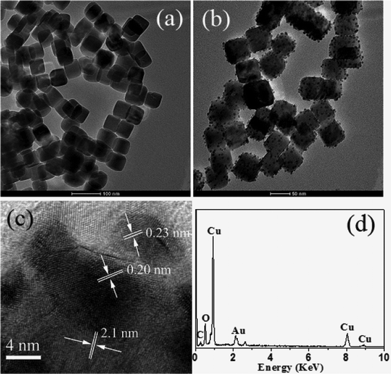 | ||
| Fig. 1 TEM images of Cu2O nanocubes before (a) and after (b) exposure to HAuCl4 precursor; HRTEM image (c); and EDS analysis (d) of as-prepared Cu2O–Au nanocomposites. | ||
In order to confirm the composition of the smaller NPs formed on the surfaces of the Cu2O nanocubes, the XPS technique was exploited. The overview XPS spectrum (Fig. 2a) displays Au 4f, Cu 2p, C 1s and O 1s peaks. The peaks (Fig. 2b) located at 83.9 and 87.6 eV are assigned to the spin–orbit split components of the Au 4f level, which matches well with the values of the zero oxidation state of metallic Au,30 confirming that the newly produced NPs are Au nanocrystals. The content of Au on the surface of the Cu2O nanocubes obtained here is about 2.50 atom%, which is consistent with the EDS analysis. The fine spectra of the Cu 2p3/2 and Cu 2p1/2 binding energies (Fig. 2c) are located at 932.48 and 952.37 eV, arising from Cu2O in the surface region. Note that the peaks ascribed to Cu2+ states, such as CuO and Cu(OH)2, were not detected obviously here. The O 1s spectrum in Fig. 2d can be resolved into two peaks. The high binding energies component at 530.1 eV indicates the formation of Cu2O phase, and the small component at 531.1 eV is ascribable to hydroxyl groups and molecular water adsorbed on the surface,31 respectively. The C 1s peak at 284.7 eV is due to adventitious carbon present in the experiment. These results demonstrate that the surface state of the Cu2O nanocubes has not changed significantly after the in situ growth of Au nanocrystals on their surfaces. The reaction between Cu2O nanocubes and Au precursor is a spontaneous redox process as a result of a large difference in the reduction potential between the Cu2+/Cu2O (0.203 V vs. SHE) pair and the AuCl4−/Au pair (0.99 V).32 Specifically, during the reduction of metal ions, a small portion of Cu(I) on the nanocubic surfaces may be oxidized to Cu(II) which will release from the solids as Cu2+ in the presence of H+ provided by HAuCl4.
 | ||
| Fig. 2 XPS spectra of as-synthesized Cu2O–Au nanocomposites: (a) overview XPS spectrum of the products; (b) Au 4f spectrum; (c) Cu 2p spectrum and (d) O 1s spectrum. | ||
To investigate the gas sensing properties of as-prepared Cu2O–Au nanocomposites, we placed a sample in a sealed chamber and measured the output voltage in air and in the presence of ethanol with concentrations from 10 to 400 ppm. The results are shown in Fig. 3a at a working temperature of 210 °C. For comparison, the sensing performances of pure Cu2O nanocubes were also investigated under the same conditions. As expected, when ethanol gas was injected into the chamber, electrical resistances for both Cu2O–Au nanocomposites and pure Cu2O nanocubes were significantly increased. The on and off characteristics of both sensors were observed when ethanol gas was injected into and taken out of the gas chamber. The response amplitudes of Cu2O–Au nanocomposites toward each concentration of ethanol were higher than those of pure Cu2O nanocubes, especially in high gas concentrations. For example, the sensitivity of the Au-decorated sensor (Fig. 3b) toward 400 ppm ethanol is estimated to be 4.34, which is much higher than that of pure Cu2O nanocubes (1.88) under the same conditions. The average response times of Cu2O nanocubes before and after Au deposition are less than 6 s, implying that the growth of Au NPs on Cu2O cube surfaces has no obvious effect on the response time to ethanol. This may be attributed to the small size of Cu2O nanocubes, that is, a large number of negatively charged oxygen ions are presented at the surface for interaction with ethanol at the working temperature. Note that the as the Cu2O nanocubes were synthesized through a surfactant-free method, a less negative effect on oxygen ionosorption will take place as a result of limited molecular species on the surfaces of the Cu2O nanocubes. Compared with the recovery time of the Cu2O nanocube-based sensor, the Au-decorated one did not require obviously more time to recover its initial resistance in the equilibrium with respect to re-absorbed surface oxygen species. This can be explained by the fact that the difference in their work functions (4.84 and 5.10 eV for Cu2O and Au, respectively) is not large enough to cause in-depth electron transfer between the sensing layer and the target molecules in this system. This point is confirmed by XPS analysis. The binding energy of Au 4f7/2 does not show an obvious shift in comparison to that of bulk Au, which is different from the results obtained from ZnO–Au nanocomposites.14 When acetone (Fig. 3c and 3d) was employed as the target gas, similar results were obtained due to their analogous sensing mechanisms.33 It is important to note that the detection limit of Cu2O–Au nanocomposites for acetone is down to 1 ppm with excellent sensitivity, which is comparable to that of n-type oxide sensors.34
 | ||
| Fig. 3 Real-time response and sensitivity curves of sensors based on pure Cu2O nanocubes (black curves/dots) and Cu2O–Au nanocomposites (red curves/dots) upon exposure to different concentrations of ethanol (a, b) and acetone (c, d) at a working temperature of 210 °C. | ||
The enhanced sensing performance of the Au-decorated sensor can be explained by the formation of deeper, continuous electron-depleted layers on the surfaces of Cu2O nanocubes. Firstly, the small diameter of the Au NPs favors a so-called spillover effect, which can enhance the sensitivity of the gas sensor. In fact, the spillover effect is the process where the newly produced oxygen atoms will migrate onto the Cu2O nanocubes forming oxygen ions, such as O−, O2− and O2−, with the assistance of Au NPs. A homogeneous distribution of Au NPs implies that dissociation of oxygen would be improved significantly on the surfaces of the Cu2O nanocubes. As a result, a deeper depletion layer is formed compared to the pure Cu2O nanocubes. Furthermore, the small size of the Cu2O nanocubes facilitates the formation of depletion layers with larger width. According to a former report,17 the change in the width of depletion layer (ΔR) can be deduced as:
| ΔR = (2εε0Δv/qNA)1/2 |
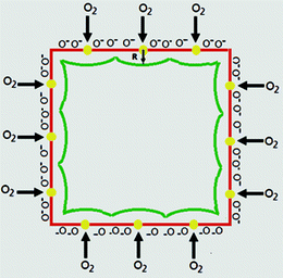 | ||
| Fig. 4 Schematic illustration for gas sensitization of Cu2O nanocubes modified with Au NPs. | ||
In conclusion, Au NPs with a narrow size distribution have been successfully grown on the surfaces of Cu2O nanocubes via a spontaneous redox reaction. The driving force for the reaction is the difference in reduction potentials between Cu2+/Cu2O and AuCl4−/Au pairs. The enhanced sensing performance of the Au-decorated sensor has been observed, which may be attributed to the effect caused by homogeneous distribution of Au NPs on nanosized Cu2O cubes. This method may be extended to the deposition of other noble metal or alloy NPs on the surface of Cu2O nanostructures in order to further improve the sensing behavior of pure Cu2O nanostructures.
Acknowledgements
This work has been supported by the National Natural Science Foundation (Nos. 21001006, 21171007 and 21105001) of P. R. China.Notes and references
- M. E. Franke, T. J. Koplin and U. Simon, Small, 2006, 2, 36 CrossRef CAS.
- X.-J. Huang and Y.-K. Choi, Sens. Actuators, B, 2007, 122, 659 CrossRef.
- D. Chen, J. Xu, Z. Xie and G. Shen, ACS Appl. Mater. Interfaces, 2011, 3, 2112 CAS.
- J. Liu, Z. Guo, F. Meng, Y. Jia, T. Luo, M. Li and J. Liu, Cryst. Growth Des., 2009, 9, 1716 CAS.
- D.-K. Ma, J.-L. Jiang, J.-R. Huang, D.-P. Yang, P. Cai, L.-J. Zhang and S.-M. Huang, Chem. Commun., 2010, 46, 4556 RSC.
- X. Lai, D. Wang, N. Han, J. Du, J. Li, C. Xing, Y. Chen and X. Li, Chem. Mater., 2010, 22, 3033 CrossRef CAS.
- J. Liu, T. Luo, F. Meng, K. Qian, Y. Wan and J. Liu, J. Phys. Chem. C, 2010, 114, 4887 CAS.
- H. Nguyen and S. A. El-Safty, J. Phys. Chem. C, 2011, 115, 8466 CAS.
- M. Tiemann, Chem.–Eur. J., 2007, 13, 8376 CrossRef CAS.
- X. Sun, J. Liu and Y. Li, Chem.–Eur. J., 2006, 12, 2039 CrossRef CAS.
- X. W. Lou, L. A. Archer and Z. C. Yang, Adv. Mater., 2008, 20, 3987 CrossRef CAS.
- J. R. Huang, K. Yu, C. P. Gu, M. H. Zhai, Y. J. Wu, M. Yang and J. H. Liu, Sens. Actuators, B, 2010, 147, 467 CrossRef.
- C. Wang, L. Yin, L. Zhang, D. Xiang and R. Gao, Sensors, 2010, 10, 2088 CrossRef CAS.
- X. Liu, J. Zhang, L. Wang, T. Yang, X. Guo, S. Wu and S. Wang, J. Mater. Chem., 2011, 21, 349 RSC.
- X. Liu, J. Zhang, X. Guo, S. Wu and S. Wang, Nanotechnology, 2010, 21, 095501 CrossRef.
- Y. Zhang, Q. Xiang, J. Xu, P. Xu, Q. Pan and F. Li, J. Mater. Chem., 2009, 19, 4701 RSC.
- C. Li, L. Li, Z. Du, H. Yu, Y. Xiang, Y. Li, Y. Cai and T. Wang, Nanotechnology, 2008, 19, 035501 CrossRef.
- J. T. Zhang, J. F. Liu, Q. Peng, X.. Wang and Y. D. Li, Chem. Mater., 2006, 18, 867 CrossRef CAS.
- H. G. Zhang, Q. S. Zhu, Y. Zhang, Y. Wang, L. Zhao and B. Yu, Adv. Funct. Mater., 2007, 17, 2766 CrossRef CAS.
- J. Liu, S. Z. Wang, Q. Wang and B. Y. Geng, Sens. Actuators, B, 2009, 143, 253 CrossRef.
- K. X. Yao, X. M. Yin, T. H. Wang and H. C. Zeng, J. Am. Chem. Soc., 2010, 132, 6131 CrossRef CAS.
- B.-X. Tang, F. Wang, J.-H. Li, Y.-X. Xie and M.-B. Zhang, J. Org. Chem., 2007, 72, 6294 CrossRef CAS.
- A. O. Musa, T. Akomolafe and M. J. Carter, Sol. Energy Mater. Sol. Cells, 1998, 51, 305 CrossRef CAS.
- L. Zhang, H. Li, Y. Ni, J. Li, K. Liao and G. Zhao, Electrochem. Commun., 2009, 11, 812 CrossRef CAS.
- P. Poizot, S. Laruelle, S. Grugeon, L. Dupont and J. M. Taracon, Nature, 2000, 407, 496 CrossRef CAS.
- W.-Y. Yang, W.-G. Kim and S.-W. Rhee, Thin Solid Films, 2008, 517, 967 CrossRef CAS.
- C. C. Li, X. M. Yin, T. H. Wang and H. C. Zeng, Chem. Mater., 2009, 21, 4984 CrossRef CAS.
- Y. Xie, K. Ding, Z. Liu, R. Tao, Z. Sun, H. Zhang and G. An, J. Am. Chem. Soc., 2009, 131, 6648 CrossRef CAS.
- H. Zhang, Y. Xie, Z. Sun, R. Tao, C. Huang, Y. Zhao and Z. Liu, Langmuir, 2011, 27, 1152 CrossRef CAS.
- S. Wang, J. Huang, Y. Zhao, S. Wang, X. Wang, T. Zhang, S. Wu, S. Zhang and W. Huang, J. Mol. Catal. A: Chem., 2006, 259, 245 CrossRef CAS.
- R. Xu and H. C. Zeng, Langmuir, 2004, 20, 9780 CrossRef CAS.
- G. Millazzo and S. Caroli, Tables of Standard Electrode Potentials, John Wiley & Sons Inc., New York, 1978 Search PubMed.
- D. Kohl, Sens. Actuators, B, 1990, 1, 158 CrossRef.
- J. Huang, Y. Wu, C. Gu, M. Zhai, Y. Sun and J. Liu, Sens. Actuators, B, 2011, 155, 126 CrossRef.
Footnote |
| † Electronic supplementary information (ESI) available: Experimental materials and procedures, XRD patterns of pure Cu2O and Cu2O–Au nanocomposites. See DOI: 10.1039/c2ra20789c |
| This journal is © The Royal Society of Chemistry 2012 |