Facile fabrication of conducting hollow carbon nanofibers/Si composites for copper phthalocyanine-based field effect transistors and high performance lithium-ion batteries
Jie
Shu
*a,
Rui
Ma
a,
Miao
Shui
a,
Ying
Wang
*b,
Nengbing
Long
a,
Dongjie
Wang
a,
Yuanlong
Ren
a,
Ruifeng
Zhang
a,
Weidong
Zheng
a and
Shan
Gao
a
aFaculty of Materials Science and Chemical Engineering, Ningbo University, Ningbo, 315211, Zhejiang Province, People's Republic of China. E-mail: sergio_shu@hotmail.com; shujie@nbu.edu.cn; Fax: +86-574-87609987; Tel: +86-574-87600787
bSchool of Material Science and Research Center for Integrated Science, Japan Advanced Institute of Science and Technology, 1-1 Asahidai, Nomi, Ishikawa, 923-1292, Japan. E-mail: wang-y@jaist.ac.jp
First published on 3rd July 2012
Abstract
In this paper, we describe the preparation and dual-use of carbon nanofibers/Si (CNFs/Si) composites as the source/drain contacts for copper phthalocyanine (CuPc) based thin film transistors (TFTs) and as anode materials for high performance lithium-ion batteries. The CNFs/Si composites are prepared by a facile chemical vapor deposition (CVD) technique with iron nitrate as the catalyst source and acetylene as the carbon source. In the CNFs/Si structure, Si particles are tightly wrapped by CNFs with an average diameter of 15–30 nm and length of 1–2 μm. It can be seen that the catalysts are grown on the top tip of the CNFs. Based on the superior properties of the CNFs coating, the CNFs/Si composites are applied in different fields. Compared with CuPc based OTFTs with Au contacts, the performances of organic thin film transistors (OTFTs) with CNFs/Si contacts are significantly improved. For OTFTs with CNFs/Si contacts, they show the on-state current increasing from 9 × 10⁻⁹ to 3 × 10⁻⁷ A at the gate voltage of −40 V, field effect mobility increasing from 1.9 × 10⁻⁴ to 4.2 × 10⁻³ cm2 V−1 s−1, and threshold voltage shifting from 15 to 30 V for the saturation regime. These are attributed to the more effective charge-carrier injection of CNFs/Si contacts than of Au contacts. Besides, the CNFs/Si composites are also promising lithium storage host materials. They show excellent rate capability as anode materials for lithium batteries. The initial discharge and charge capacities of CNFs/Si composites at 0.05 C are 1491.6 and 1168.7 mAh g−1, respectively. For comparison, the initial discharge and charge capacities of the CNFs/Si composites at 0.60 C are 1197.8 and 941.4 mAh g−1, respectively. After twenty cycles, the discharge and charge capacities at 0.60 C are 834.4 and 733.9 mAh g−1, respectively.
1. Introduction
In the last decade, multi-functional materials have been an important factor in many fields, such as energy storage, and solid state devices. Thus, they have attracted much attention and enormous efforts have been devoted to the synthesis of new multi-functional materials, in both academic and industrial laboratories. Among multi-functional materials for different applications, solution-processed highly conductive electrode materials are desirable due to their wide applications. However, the yet reported multi-functional solution-processed materials with high conductivity are still limited and cannot meet the needs of the modern world.Conducting carbon mixing or coating is an efficient technique to improve the electronic conductivity of active materials for lithium-ion batteries. For conducting carbon mixing, acetylene black (AB), carbon black (CB), carbon fiber (CNF) or carbon nanotubes (CNT) are always used and added to the active materials by high energy ball-milling. For conducting carbon coating, an amorphous carbon layer, CNF or CNT is always formed on the surface of the active materials by thermal decomposition of carbon-containing organic compounds. Among all the conducting carbon materials, CNT is an one-dimensional material with a hollow tube including a curled graphene structure and an end cap with a hemispherical fullerene structure. The peculiar structure means CNTs have different physical and chemical characteristics. Due to their high electronic and thermal conductivities, and excellent mechanical and chemical stabilities, CNTs are always used as conducting additives in lithium-ion batteries. In previous reports, we preliminarily explored the possibility of fabricating cage-like composites with CNTs as anode materials for lithium ion batteries.1,2 It was found that putting active materials into the CNTs cage can improve the electrochemical properties of the electrodes, especially for Si particles. Furthermore, CNTs are also good lithium storage candidate materials with a reversible capacity of around 200 mAh g−1. Following lithium ion insertion into a CNTs structure, lots of solvent will decompose and deposit onto the surface of CNTs. Due to their large specific surface area, the irreversible capacity of CNTs is huge.1 Similar to the physical/chemical properties of CNTs, CNFs also have high electronic, thermal conductivities, and excellent mechanical and chemical stabilities. However, CNFs are almost electrochemically inactive materials for lithium storage. Therefore, this may inhibit some side reactions during charge–discharge processes. Using CNFs as the building material, urchin-like nature graphite/CNFs, carbon sphere/CNFs, Si/CNFs and Cr2O3/CNFs composites can be prepared by a thermal chemical vapor deposition method.3–6 Fabricated as anode materials for lithium-ion batteries, these urchin-like composites show improved electrochemical performances after CNFs coating. However, the fabricating of Si/CNFs is associated with a pre-coating with pyrolytic carbon on Si particles. It is a complex method for material preparation, but otherwise many of the Si particles cannot be wrapped by the CNFs.5,6 In our previous studies, the CNTs are grown on the surface of Si particles with a pre-deposition of Ni–P alloys by a complex chemical bath method.1 It is too complicated and high-cost for the nano/micro-structured composite fabrication of lithium-ion batteries. Therefore, it is necessary to develop a facile technique to fabricate the CNFs/Si composites in a simple manner.
Organic thin film transistors (OTFTs) are the critical components of future organic electronics and will enable cheap, flexible and solution-processed low-end storage, flat panel displays and chemical sensors.7,8 A great deal of effort is being devoted to increasing their key performance parameters, including carrier mobility, on/off ratio and threshold voltage. By far, most effort has mainly focused on the synthesis of new organic semiconductors and dielectrics and the deposition of the semiconductors,9–11 but the contact between the electrodes and the active layer has not received much attention. As carrier injection from the source/drain contacts (one of the essential components of the OTFTs) into the active semiconducting layer is also critical for OTFTs performance,12–14 the study of materials that can be used as the drain and source contacts is of equal importance. In most reported OTFTs, source and drain contacts mainly use vacuum-deposited noble-metal contacts or solution-processed intrinsically conductive molecular or polymeric contacts. However, the use of noble metal contacts (such as gold) runs counter to the low-cost approach of organic electronics. Firstly, it mainly is deposited by vacuum deposition methods (such as sputtering or evaporation) instead of less-expensive solution methods (such as printing and casting). Secondly, though other methods instead of vacuum deposition, such as electroplating and inkjet printing of noble metal nanoparticles, have been used to deposit noble metal contacts,15 noble metals are very expensive and their adhesion to organic materials is not good. Lastly, physical damage from deposited metal contacts, or metal–semiconductor reactions may also influence the contact resistance. Therefore, intrinsically conductive molecules or polymers are more preferable. Conducting polymers have been widely used as source/drain contacts.16,17 Nevertheless, available conducting materials tend to degrade when they are exposed to ambient air and their high resistivities, relative to metal contacts, compromise the performance of the OTFTs devices. High-resolution printable conducting polyaniline nanotube composites have been prepared and shown a high conductivity of 2 S cm−1. Pentacene-based OTFTs using them as contacts showed a high mobility of 0.20 cm2 V−1 s−1 and logic gates exhibited gains greater than 10.18a Nevertheless, solution-processed conducting materials as the contacts of OTFTs are scarce and will be of great scientific and technological interest for the future. CNFs/Si composites for lithium ion batteries have high conductivity and a very interesting structure; Si particles wrapped by CNFs. It has been reported that CNTs can be used as the electrode materials of OTFTs and the devices show good performance.18b Here, the CNFs/Si composites have a high conductivity and the CNFs on the Si particles probably have good contact with the organic semiconductors. This inspired us to use the CNFs/Si composites as the electrode materials for OTFTs.
In this paper, we report on the characteristics and properties of multi-functional materials; CNFs/Si composites. The applications of CNFs/Si composites as the source/drain contact of the CuPc based TFTs and anode materials for lithium-ion batteries are thoroughly studied. It is found that the CuPc based TFTs using CNFs/Si as contacts show an on-state current of 3 × 10⁻⁷ A at a gate voltage of −40 V, field effect mobility of 4.2 × 10⁻³ cm2 V−1 s−1, and threshold voltage shifting of 30 V for the saturation regime. Similarly, the anode fabricated by CNFs/Si shows a reversible capacity of 733.9 mAh g−1 and a capacity retention of 77.9% at 0.60 C after twenty cycles, which is better than the previous reported results.13,16,18a
2. Experimental
2.1. Fabrication and characterization of CNFs/Si
Before use, commercial Si particles (Sinopharm Chemical Reagent Shanghai Co., Ltd, China) are ball-milled for 10 h to reduce the particle size. A solution of Fe(NO3)3 is prepared by putting 30 g Fe(NO3)3·9H2O (Sinopharm Chemical Reagent Shanghai Co., Ltd, China) into 100 mL distilled water. After high energy ball-milling, 20 g Si powder is dispersed into the Fe(NO3)3 solution with a constant solution temperature of 50 °C, then the mixing solution is continuously stirred for 5 h. After filtration, the precipitate is dried at 100 °C for 12 h in a vacuum oven. The resulting product is ground by a mortar and pestle. For CNFs growth, the resulting product is put into a tube furnace equipped with mixed gases of acetylene, hydrogen and argon (C2H2/H2/Ar = 1![[thin space (1/6-em)]](https://www.rsc.org/images/entities/char_2009.gif) :1:9, v/v/v). CNFs/Si composites can be obtained by a thermal chemical vapor deposition at 550 °C for 1 h. The morphologies and components of samples are characterized by means of a Hitachi S-3400 scanning electron microscopy (SEM) equipped with a Bruker energy dispersive X-ray spectroscopy (EDS). The fine grain structures of samples are observed with a JEOL JEM-2100 high resolution transmission electron microscopy (HRTEM).
:1:9, v/v/v). CNFs/Si composites can be obtained by a thermal chemical vapor deposition at 550 °C for 1 h. The morphologies and components of samples are characterized by means of a Hitachi S-3400 scanning electron microscopy (SEM) equipped with a Bruker energy dispersive X-ray spectroscopy (EDS). The fine grain structures of samples are observed with a JEOL JEM-2100 high resolution transmission electron microscopy (HRTEM).
2.2. Preparation of CuPc based TFTs
The fabrication of CuPc based OTFTs starts with a heavily n-doped silicon substrate with 450 nm thermal SiO2 as the gate insulator. A 50 nm thick CuPc active layer is deposited on the surface of SiO2 at a fixed rate of 1 Å s−1 by vapor deposition under pressure of 4 × 10⁻⁵ Pa. The substrate is held at room temperature during the deposition. The contacts of carbon nanotubes/Si composites are deposited by drop casting a mixture of active materials and polyvinylidene fluoride dissolved in N-methyl-pyrrolidone, defining a channel length (L) of 4 mm and a channel width (W) of 13 mm. For comparison, the Au source/drain contacts are deposited on the CuPc active layer through a shadow mask by vacuum evaporation, defining the same channel length and width. Finally, all OTFTs are characterized at room temperature using a Hewlett–Packard 4140B semiconductor parameter analyzer at different gate voltages, without any precautionary measures being taken to isolate the devices from exposure to ambient oxygen and moisture.2.3. Preparation of lithium-ion batteries
For electrochemical analysis, the working electrode is fabricated by mixing the as-prepared materials with additives. The pure Si electrode is composed of Si powder (80 wt.%), acetylene black (10 wt.%) and polyvinylidene fluoride (10 wt.%). The CNFs/Si electrode is composed of CNFs/Si composites (90 wt.%) and polyvinylidene fluoride (10 wt.%). Polyvinylidene fluoride is dissolved in N-methyl-pyrrolidone to form an organic solution. After mixing the active materials and additives, an homogeneous slurry can be obtained. The working electrode is prepared by casting the slurry on a copper foil by a doctor blade technique. After casting, the film is dried at 120 °C for 12 h in a vacuum oven, then cut into discs with a diameter of 15 mm. For electrochemical cycling, the simulated battery is assembled by using the as-prepared working electrode as the cathode, a Whatman glass fiber filter as separator, a metal lithium disc as anode and 1 mol L−1 LiPF6 dissolved in a mixture of ethylene carbonate and dimethyl carbonate (1:1, v/v) as the electrolyte in an Etelux Ar-filled glove box. All the charge–discharge cycles are tested on a multi-channel Land battery testing system at room temperature.
3. Results and discussion
3.1. Growth process and characteristic of CNFs/Si composites
Fig. 1(a)–1(e) show the morphology of Si particles after high energy ball-milling for 10 h. The sample is composed of irregular Si particles. The size of the Si particles ranges from 0.5 to 3 μm. Whether the particles are spheres or blocks, the Si particles are well-crystallized samples with an amorphous SiO2 layer on the surface as the HRTEM images shown in Fig. 1(b)–1(e). After soaking in aqueous Fe(NO3)3 solution for 5 h, the surface of the Si particles is loaded by plenty of small catalysts with an average particle size of 10–20 nm as the SEM images show in Fig. 1(f) and 1(g). EDS results in Fig. 1(h) shows that these catalysts are iron oxides. After a thermal chemical vapor deposition, the Si particles are wrapped tightly by carbon nanofibers as the EDS, SEM and HRTEM images show in Fig. 1(i)–(p). In the experiments, coiled CNFs are grown on the Si particles and crosslinked mutually. This is different from the previous results reported by ref. 5 & 6. They find that it is difficult to form a well-wrapped CNFs/Si composite without pre-treatment, such as a pyrolytic carbon coating on Si particles. In contrast, all the Si particles are thoroughly wrapped by CNFs with Fe-based catalysts directly loading on the Si particles. The Si particles are out-of-sight. Besides, it can also be seen that the catalysts are grown on the top tip of the CNFs. These hollow CNFs show a turbostratic graphite structure with a diameter of 15–30 nm and length of 1–2 μm. As a result, the Si particles are put into CNFs-fabricated cages. The image in Fig. 1(i) shows that the CNFs/Si composites are distributed uniformly and form a continuous film. Between the CNFs/Si composites, coiled CNFs from different cages are also crosslinked mutually and make all the CNFs/Si composites connect with each other. It seems that Si particles are embedded in a three-dimensional network of CNFs.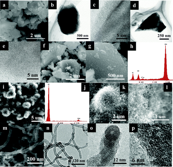 | ||
| Fig. 1 SEM, HRTEM and EDS images of Si particles (a)–(e), catalysts/Si composites (f)–(h) and CNFs/Si composites (i)–(p). | ||
The whole growth process of CNFs/Si composites is illustrated in Fig. 2. It indicates that the preparation method of CNFs/Si composites is a facile technique. According to the previous reports,19–21 it is known that Si material is a promising lithium storage anode material with a theoretical capacity of 4200 mAh g−1. However, pure Si powder shows a poor cycling calendar life and low reversible capacity for large volume changes during lithiation–delithiation reactions. Therefore, it is expected that the electrochemical properties of CNFs/Si composites may be improved by putting Si particles into CNFs cages. As is well-known, the application of OTFTs is always limited to the use of noble metal contacts and their fabrication techniques. As a result, many kinds of conducting materials have been tried as source/drain contacts.16,17 Here, CNFs/Si composites are fabricated by a CNFs coating layer with high electronic conductivity. It indicates that CNFs/Si composites may be good candidate materials as source/drain contacts for OTFTs. Based on this novel structure, it is expected that CNFs/Si composites will be multi-functional materials in these application fields.
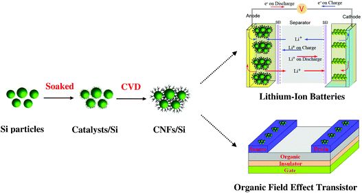 | ||
| Fig. 2 Schematic view of the preparation process of CNFs/Si composites and their applications. | ||
3.2. Application in organic thin film transistors
Fig. 3(a) and 3(b) illustrate the schematic cross section of OTFTs in a conventional top contact with different source/drain contacts. Fig. 4(a) and (b) shows the drain-to-source current (IDS) as a function of drain-to-source voltage (VDS) of the CuPc TFTs with CNFs/Si composites and Au as the source/drain contacts, respectively. All devices show good output characteristics with classical linear/saturation response. At a gate voltage (VGS) of 0 V, IDS is very small and the OTFTs operate in the accumulation mode with excellent current saturation at higher VDS. The large output impedance, achieved at the saturation regime, is desirable in electronics applications. For these devices, enhancement of the saturation current is seen as a function of increasing gate voltage in Fig. 4.These results demonstrate that the CNFs/Si composites, same as Au, can be effectively used as the source/drain contacts of OTFTs. Under a gate voltage of −40 V, for the CuPc based OTFTs with the CNFs/Si contacts a high saturation current of more than 3 × 10⁻⁷ A was achieved, which is relatively high compared to the value, 9 × 10⁻⁹ A, of the CuPc based OTFTs using Au electrodes. In the saturation regime, the field effect mobility (μFE) of the OTFTs can be calculated from the slope of the plot of |IDS|1/2vs. VGS in the saturation field region (VDS=−80 V) by the eqn:| IDS = (WCi/2L)μFE(VGS − VT) | (1) |
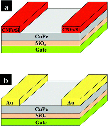 | ||
| Fig. 3 Schematic view of the OTFTs with CNFs/Si contacts (a) and Au contacts (b). | ||
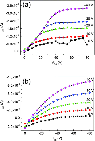 | ||
| Fig. 4 The output characteristics of the CuPc based OTFTs with CNFs/Si contacts (a) and Au contacts (b). | ||
where L is the channel length, W is the channel width, Ci is the capacitance per unit area of the insulating layer, VT is the threshold voltage, and μFE is the field effect mobility. The threshold voltage was calculated from the x-axis intercept of the square root of the IDSvs. VGS plot. The CuPc based OTFTs with Au affording mobile contacts are inferior, relative to the reported performance of CuPc OTFTs with Au contacts and SiO2 insulator.22,23 The substrate was not heated during evaporation and the channel length was rather long, which may result in inferior performance because of numerous CuPc grain boundaries. Comparing the two groups of data shown in Table 1, OTFTs with the CNFs/Si contacts have a twentyfold increase of field-effect mobility and a 15-V shift of the threshold voltage in the positive direction. The VT of the devices with different source/drain contacts are 15 V and 30 V, respectively. VT is a measurement of the amount of charge that must be electrostatically induced to switch on the electrical conduction in OTFTs and its magnitude depends on the quality of the source/drain contacts. A 15-V shift of the threshold voltage in the positive direction suggests that little induced holes are needed to switch on the OTFTs. Since the difference between the two OTFTs is just the material that is used for the source/drain contacts, we believe that the reason for the improved performance can be attributed to the better hole injection of CNFs/Si contacts than that of Au contacts. A similar improvement of the performance of the OTFTs has been achieved by improving charge-carrier injection using a lutetium bisphthalocyanine buffer layer between the Au contacts and CuPc film.24a Using the CNFs/Si composite contacts, it is inferred that the contact between CNFs and CuPc films is the main contact between the contacts and CuPc films, as the silicon particles are wrapped by the coiled CNFs cage, as shown in Fig. 1(i). As the CNFs composed of six-membered rings, a strong van der Waals force connection between the source/drain contacts and CuPc film can be expected, resulting in an effective charge injection from the contacts to the CuPC films. However, the deposition of Au will form a metallic overlayer, which is a mixture of metal and organic semiconductor. The interface dipole forms an increasing barrier height between the Au contacts and CuPc, which results in poor charge-injection.
| Source/drain electrodes | Capacitance of SiO2 dielectric/nF cm−2 | Mobility/cm2 V−1 s−1 | On/off ratio | Threshold potential/V |
|---|---|---|---|---|
| CNFs/Si contacts | 10 | 4.2 × 10⁻³ | 62 | 30 |
| Au contacts | 10 | 1.9 × 10⁻⁴ | 15 | 15 |
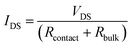
Poor charge injection into the semiconductor layer affects the electrical characteristics of the device in the linear region. In order to understand further the difference in the charge injection properties (contact resistance) of the devices with different contacts, Fig. 5(a) and (b) shows the plots of IDSvs. VDS at constant VGS of 0 V and −40 V from 0 V to −35 V, respectively. The slopes of the two curves indicate a total resistance (Rtotal) of OTFTs including the contact resistance and the bulk resistance. The IDS is proportional to the total resistance (Rtotal) between the source and drain contacts:
 | (2) |
 | ||
| Fig. 5 The plots of IDSvs. VDS at constant VGS of 0 V (a) and−40 V (b) from 0 V to−35 V of the CuPc based OTFTs. | ||
where Rcontact and Rbulk represent the contact resistance and bulk resistance, respectively. Rbulk depends on the number of charge carriers in the semiconductor layer and thus is influenced by VGS. As seen from Fig. 5(a), it is found that a substantial current, about 6 × 10⁻⁸ A at −35 V, flows through the CNFs/Si contacts at zero gate voltage, which indicates a relatively high conductivity. The current flowing through the Au contacts is only about 1.8 × 10⁻¹⁰ A at −35 V. The total resistance at a VGS of 0 V is about 4.6 × 10¹⁰ Ω for the device with CNFs/Si contacts and 1.7 × 10¹² Ω for the device with Au contacts by linear fitting of the two curves, respectively. When the devices are applied with a zero gate voltage both devices are all on-state because the threshold voltages of both devices are positive. The organic semiconductors generally have very high resistivities and Rcontact is relatively small, especially for the wide conductive channel of the devices. So it is reasonable that Rbulk, which is directly dependent on the number of charge carriers, dominates Rtotal because both CuPc films are grown at the same condition and then have similar traps. Rbulk with Au contacts is larger than Rbulk with CNFs/Si contacts, so the lower Rbulk results from more holes easily injected from the CNFs/Si contacts. Moreover, the threshold voltage of the devices with CNFs/Si composites is more positive than that of the devices with Au, which is consist with that of the devices with lower injection barrier.24b Although the contact resistance is not assessed quantitatively, in this case due to the problem of fabrication, all results show that the CNFs/Si contacts have a much lower contact resistance than Au contacts.
3.3. Application in lithium-ion batteries
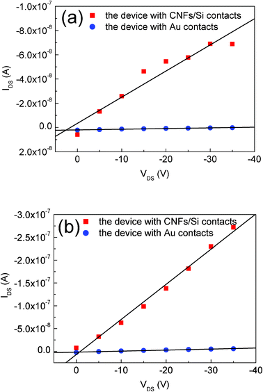
Fig. 6(a) and 6(b) show the charge–discharge and corresponding dQ/dV curves of pure Si and CNF/Si composites at different charge–discharge rates. The initial discharge and charge capacities of pure Si are 3906.8 and 2566.1 mAh g−1, respectively. This suggests that Si-based materials will be promising anode candidates for lithium-ion batteries. The electrochemical reactions between Li and Si always result in the formation of successive Li–Si alloys, such as Li12Si7, Li14Si6, Li13Si4 and Li22Si5. According to a maximum lithium storage capacity of Li22Si5, the volume expansion of an Si particle is calculated to be as high as 400%. This induces the cracking and pulverization of Si particles, then the disintegration of the electrode. As a result, the capacity retention of pure Si is poor. Viewed from dQ/dV curves, it is obvious that the reduction and oxidation peaks of pure Si disappear at the 5th and 10th cycles. After twenty cycles, the discharge and charge capacities of pure Si are merely 162.2 and 134.4 mAh g−1, respectively. To suppress the volume change of pure Si, an effective approach is to narrow the cycling potential window.25,26 Based on this method, the volume expansion and shrinkage can be restricted by limiting of lithium storage content in Si particles. Here, conducting hollow CNFs are introduced to improve the electrochemical properties of Si particles.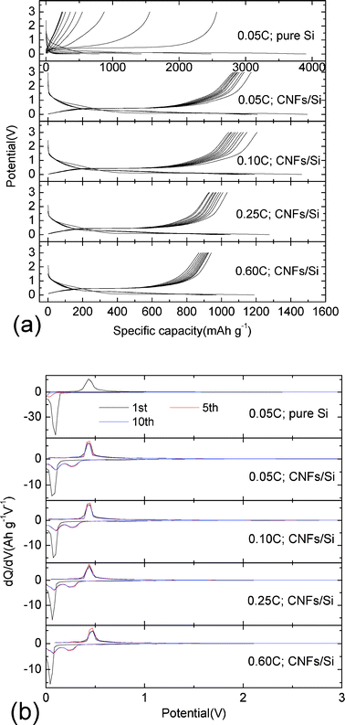 | ||
| Fig. 6 Charge–discharge curves and corresponding dQ/dV curves of pure Si and CNFs/Si composites at different rates (0.05 C, 0.10 C, 0.25C and 0.60 C) in 0.0–3.0 V. | ||
As shown in Fig. 6(a), CNFs/Si composites exhibit improved electrochemical properties at a charge–discharge rate of 0.05 C. The initial discharge and charge capacities of CNFs/Si composites are 1491.3 and 1173.5 mAh g−1, respectively. After twenty cycles, the discharge and charge capacities are 868.1 and 788.2 mAh g−1, respectively. From the 2nd to 10th cycles, it is also found that the dQ/dV curves of CNFs/Si composites maintain similar reduction and oxidation peaks at 0.05 C. These results show that the volume change of Si particles is effectively suppressed by CNFs coating. During the lithiation and delithiation process, CNFs layer acts as a buffer to relieve the mechanical stresses inside the Si particles. Based on previous studies, it is known that most Si/C composites always show advanced electrochemical properties in a narrow potential window, such as 0.02–1.2 V.25–30 This is why the degree of lithium storage in Si particles is limited, to suppress the volume change of active materials. In contrast, the CNFs/Si composites fabricated in this experiment can be cycled in a broad electrochemical window 0.0–3.0 V. The cycling calendar life and reversible capacity of CNFs/Si composites in 0.0–3.0 V are as good as those delivered by other reported Si/C composites in 0.02–1.2 V. This indicates that crosslinked CNFs coating may provide a solid cage stronger than the continuous carbon layer on the surface of Si particles. Therefore, as-prepared CNFs/Si composites are promising anode candidate materials for lithium-ion batteries.
Rate performance is an important factor for lithium-ion batteries in the field of practical applications. Although the rate performances of carbonaceous materials have been widely reported, high rate behavior of Si-based materials has been rarely described over the past several decades. This is because lots of lithium ions inserting into Si particles in a short time will induce the non-uniform distribution of mechanical stresses inside the Si particles. As a result, the Si particles are vulnerable to suffer cracking and pulverization, then electronic contact loss. In our experiment, the CNFs/Si composites were cycled at rates of 0.05 C, 0.10 C, 0.25 C and 0.60 C in a potential range of 0.0–3.0 V. It is expected that a CNFs/Si composite could show superior rate performance by using crosslinked CNFs as a buffer and a three-dimensional conducting network. Fig. 6(a) shows the charge–discharge curves of CNF/Si composites at different rates. It is obvious that not only the cycling calendar life but also the rate properties are improved by introducing the CNFs coating. In the cage-like CNFs/Si composites, plenty of crosslinked CNFs provide many electronic conducting bridges between Si particles and the current collector for electron transportation. Furthermore, the CNFs cage has a three-dimensional network structure with lots of channels allowing lithium ion transportation without obstacle. As a result, the charge–discharge curves at a rate as high as 0.6 C show similar behavior to those obtained at 0.05 C. As displayed in Fig. 6(a), the charge–discharge curves of CNFs/Si composites at 0.60 C exhibit the typical Li lithiation–delithiation characteristics of Si/C composite materials. Viewed from the dQ/dV curves in Fig. 6(b), it can be found that there are two reduction peaks located at around 0.08 and 0.25 V and one oxidation peak located at around 0.44 V for all the samples at different rates (0.05 C, 0.10 C, 0.25 C and 0.60 C). This is consistent with the equilibrium potentials of electrochemical reactions between lithium ions and Si materials, which are 0.05, 0.16, 0.29 and 0.35 V.21,31 Therefore, these novel CNFs/Si composites may be suitable as lithium storage anode materials.
Fig. 7(a) and 7(b) shows the comparative charge–discharge curves and cycling performances of pure Si and CNFs/Si composites at different rates (0.05 C, 0.10 C, 0.25 C and 0.60 C). Based on the typical charge–discharge curves, there are two lithiation potential platforms and one delithiation potential platform, which correspond to the reduction and oxidation peaks in dQ/dV curves as shown in Fig. 6(b). With an increase of charge–discharge rates from 0.05 C to 0.60 C, two lithiation platforms in Fig. 7(a) shift from 0.266, 0.096 V (0.05 C) to 0.259, 0.101 V (0.10 C), 0.246, 0.083 V (0.25 C) and 0.240, 0.073 V (0.60 C). The delithiation platform increases from the potential at 0.427 V (0.05 C) to 0.432 V (0.10 C), 0.439 V (0.25 C) and 0.463 V (0.60 C). Although the charge–discharge rate is increased from 0.05 C to 0.60 C, the charge and discharge polarization potentials are merely 0.036 and 0.024 V, respectively. This indicates that the crosslinked CNFs coating is very effective to enhance the electronic conductivity between Si particles and the current collector. On the other side, the discharge and charge capacities of CNFs/Si composites are almost the same values at different rates. Therefore, the improved rate capability can be also ascribed to the robust micro/nano-structure. Compared with pure Si, the reversible capacity, cycling calendar life and capacity retention are greatly enhanced for the cage-like CNFs/Si composites as shown in Fig. 7(b). The reversible capacity of CNFs/Si composites at 0.05 C, 0.10 C, 0.25 C and 0.60 C are 788.2, 766.8, 692.6 and 733.9 mAh g−1, respectively. The capacity retentions of CNFs/Si composites at 0.05 C, 0.10 C, 0.25 C and 0.60 C are 67.3, 63.6, 67.1 and 77.9%, respectively. For comparison, the reversible capacity and capacity retention of pure Si are merely 162.2 mAh g−1 and 6.3%, respectively. In previous studies,1 the improved electrochemical properties of carbon nanotubes/Si composites contribute to the three-dimensional conducting carbon nanotube network and continuous solid electrolyte interphase (SEI) film as the elastic buffer. Here, the SEM images of two kinds of electrodes after twenty cycles are shown in Fig. 8(a) and 8(b). It is found that the cracking and pulverization of Si particles can also be effectively suppressed by the crosslinked CNFs coating, as shown in Fig. 8(a)–8(c). However, few SEI films can be observed on the surface of CNFs/Si composites, as shown in Fig. 8(b). The SEI free characteristics of CNFs are probably attributed to the electrochemically inactive behavior during the charge–discharge cycles. Therefore, crosslinked CNFs should be solely responsible for the advanced rate performance of CNFs/Si composites. After repeated electrochemical cycles, the Si particles are tightly wrapped by crosslinked CNFs, which provides cage-like micro/nano-structures acting as holder of chemical/mechanical robustness to suppress the volume expansion of Si particles. As a result, CNFs/Si composites show superior electrochemical properties as anode materials for lithium-ion batteries.
 | ||
| Fig. 7 Comparative charge–discharge curves (a) and cycling performances (b) of CNFs/Si composites at different rates (0.05 C, 0.10 C, 0.25C and 0.60 C) in 0.0–3.0 V. | ||
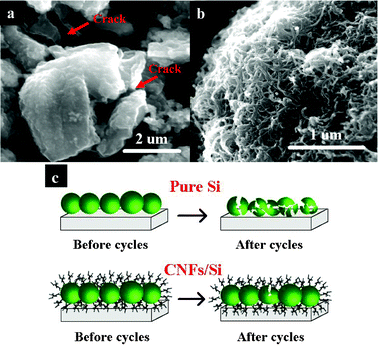 | ||
| Fig. 8 SEM images of pure Si (a) and CNFs/Si (b) electrodes after cycles and their schematic view before and after cycling (c). | ||
4. Conclusions
Novel CNFs/Si composites are fabricated by soaking Si particles in Fe(NO3)3 solution followed by a thermal CVD process. In the CNFs/Si structure, the Si particles are tightly wrapped by CNFs with an average diameter of 15–30 nm and length of 1–2 μm. It can be seen that the catalysts are grown on the top tip of CNFs. CuPc based OTFTs with CNFs/Si composites as the source/drain contacts are fabricated. Our results indicate that CuPc based OTFTs with CNFs/Si composites as the source/drain contacts are superior to comparable devices fabricated using Au when tested under the same conditions. Compared with CuPc based TFTs using Au contacts, the use of CNFs/Si contacts leads to on-state current increases from 9 × 10⁻⁹ to 3 × 10⁻⁷ A at the gate voltage of −40 V, the field effect mobility increases from 1.9 × 10⁻⁴ to 4.2 × 10⁻³ cm2 V−1 s−1, and the threshold voltage shifts from 15 to 30 V for the saturation regime. Our promising results suggest that solution processed CNFs/Si composites can be used as source/drain contacts of CuPc based OTFTs and have more effective charge injection and lower contact resistance than Au contacts. This also indicates that solution processed CNFs/Si composites are a viable alternative to Au for CuPc based TFTs, eliminating the vacuum deposition of Au in the fabrication. In addition the lithium storage performance of CNFs/Si composite is also discussed in this paper. It is found that CNFs/Si composites show superior electrochemical properties as anode materials for lithium batteries. A reversible charge capacity of 733.9 mAh g−1 can be delivered at 0.60 C after twenty cycles and the capacity retention is as high as 77.9%. Excellent lithium storage behavior is attributed to crosslinked CNFs coatings. They not only provide electronic conducting bridges between Si particles and the current collector for electron transportation but also acts as a buffer to suppress the volume expansion of Si particles during lithiation and delithiation reactions. These results show that cage-like CNFs/Si composites play a vital factor in multi-functional materials and their applications.Acknowledgements
This project is sponsored by 973 Fundamental Research Program (No. 2010CB635116), National Science Foundation of China (No. 51104092), Key Project of Chinese Ministry of Education (No. 210083), Qianjiang Talent Project of Zhejiang Province (2011R10089) and the Scientific Research Foundation for the Returned Overseas Chinese Scholars, State Education Ministry. The work is also supported by Hulan Excellent Doctoral Fund and K. C. Wong Magna Fund in Ningbo University.References
- J. Shu, H. Li, R. Yang, Y. Shi and X. J. Huang, Electrochem. Commun., 2006, 8, 51 CrossRef CAS.
- J. Shu, Electrochem. Solid-State Lett., 2008, 11, A219 CrossRef CAS.
- H. L. Zhang, Y. Zhang, X. G. Zhang, F. Li, C. Liu, J. Tan and H. M. Cheng, Carbon, 2006, 44, 2778 CrossRef CAS.
- C. W. Huang, C. H. Hsu, P. L. Kuo, C. T. Hsieh and H. Teng, Carbon, 2011, 49, 895 CrossRef CAS.
- S. M. Jang, J. Miyawaki, M. Tsuji, I. Mochida and S. H. Yoon, Carbon, 2009, 47, 3383 CrossRef CAS.
- H. P. Liu, W. M. Qiao, L. Zhan and L. C. Ling, New Carbon Mater., 2009, 24, 124 CrossRef CAS.
- C. D. Dimitrakopoulos and P. R. L. Malenfant, Adv. Mater., 2002, 14, 99 CrossRef CAS.
- H. Sirringhaus, Nat. Mater., 2003, 2, 641 CAS.
- Y. Li, Y. Wu, S. Gardner and B. S. Ong, Adv. Mater., 2005, 17, 849 CrossRef CAS.
- A. Facchetti, M. H. Yoon and T. J. Marks, Adv. Mater., 2005, 17, 1705 CrossRef CAS.
- M. Chikamatsu, S. Nagamatsu, Y. Yoshida, K. Saito, K. Yase and K. Kikuchi, Appl. Phys. Lett., 2005, 87, 203504 CrossRef.
- B. H. Hamadani and D. Natelson, J. Appl. Phys., 2005, 97, 064508 CrossRef.
- J. Z. Wang, J. F. Chang and H. Sirringhaus, Appl. Phys. Lett., 2005, 87, 083503 CrossRef.
- C. W. Chu, S. H. Li, C. W. Chen, V. Shrotriya and Y. Yang, Appl. Phys. Lett., 2005, 87, 193508 CrossRef.
- Y. Li, Y. Wu and B. S. Ong, J. Am. Chem. Soc., 2005, 127, 3266 CrossRef CAS.
- K. Saito and S. Kobayashi, Appl. Phys. Lett., 2002, 80, 1489 CrossRef CAS.
- M. Halik, H. Klauk, U. Zschieschang, T. Kriem, G. Schmid, W. Radlik and K. Wussow, Appl. Phys. Lett., 2002, 81, 289 CrossRef CAS.
- (a) M. Lefenfeld, G. Blanchet and J. A. Rogers, Adv. Mater., 2003, 15, 1188 CrossRef CAS; (b) C. M. Aguirre, C. Ternon, M. Paillet, P. Desjardins and R. Martel, Nano Lett., 2009, 9, 1457 CrossRef CAS.
- A. Magasinski, P. Dixon, B. Hertzberg, A. Kvit, J. Ayala and G. Yushin, Nat. Mater., 2010, 9, 353 CrossRef CAS.
- C. K. Chan, H. Peng, G. Liu, K. McIlwrath, X. F. Zhang, R. A. Huggins and Y. Cui, Nat. Nanotechnol., 2007, 3, 31 CrossRef.
- R. A. Huggins, J. Power Sources, 1999, 81–82, 13 CrossRef CAS.
- Z. Bao, A. J. Lovinger and A. Dodabalapur, Appl. Phys. Lett., 1996, 69, 3066 CrossRef CAS.
- K. Xiao, Y. Liu, Y. Gui and B. Zhu, Appl. Phys. A: Mater. Sci. Process., 2003, 77, 367 CrossRef CAS.
- (a) J. Wang, H. Wang, J. Zhang, X. Yan and D. Yan, J. Appl. Phys., 2005, 97, 026106 CrossRef; (b) Chong-an Di, Gui Yu, Yunqi Liu, Xinjun Xu, Dacheng Wei, Yabin Song, Yanming Sun, Ying Wang, Daoben Zhu, Jian Liu, Xinyu Liu and Dexin Wu, J. Am. Chem. Soc., 2006, 128(51), 16418–16419 CrossRef CAS.
- H. Li, X. J. Huang and L. Q. Chen, Electrochem. Solid-State Lett., 1999, 2, 547 CrossRef CAS.
- U. Kasavajjula, C. S. Wang and A. J. Appleby, J. Power Sources, 2007, 163, 1003 CrossRef CAS.
- Z. P. Guo, E. Milin, J. Z. Wang, J. Chen and H. K. Liu, J. Electrochem. Soc., 2005, 152, A2211 CrossRef.
- I. S. Kim and P. N. Kumta, J. Power Sources, 2004, 136, 145 CrossRef CAS.
- Y. X. Zhang, P. K. Patil, C. Wang, A. J. Appleby, F. E. Little and D. L. Cocke, J. Power Sources, 2004, 125, 206 CrossRef.
- Y. Liu, K. Hanai, J. Yang, N. Imanishi, A. Hirano and Y. Takeda, Solid State Ionics, 2004, 168, 61 CrossRef CAS.
- S. C. Lai, J. Electrochem. Soc., 1976, 123, 1763 CrossRef.
| This journal is © The Royal Society of Chemistry 2012 |