DOI:
10.1039/C2RA20758C
(Paper)
RSC Adv., 2012,
2, 10968-10976
Nanostructured organic–inorganic heterojunction diodes as gas sensors
Received
23rd April 2012
, Accepted 6th September 2012
First published on 11th September 2012
Abstract
Nanostructured organic–inorganic heterojunction devices were fabricated by employing n-type zinc sulphide (ZnS) grown on ITO by RF magnetron sputtering and thin film of zinc phthalocyanine (ZnPc) deposited on the top of the ZnS layer by thermal evaporation. On the top of the ZnPc layer, an Al film was coated to form an electrode. Thin films of ZnS and ZnPc were characterized by optical absorption and Field Emission Scanning Electron Microscopy (FESEM). Current–voltage (I–V) characteristics of the fabricated ITO/ZnS/ZnPc/Al hetero-structures were studied at different temperatures (30 to 90 °C) in vacuum and diode-like behaviour was observed. In the case of single layer devices ITO/ZnS/Al and ITO/ZnPc/Al diode-like behavior was not obtained. The effects of donor ammonia and acceptor oxygen gases on the electrical properties of single layer devices ITO/ZnS/Al, ITO/ZnPc/Al and ITO/ZnS/ZnPc/Al heterojunctions were studied in order to investigate the utility of these devices as gas sensors. A drastic increase in forward current of the heterojunction has been noticed in the presence of donor ammonia gas containing water vapor, while a decrease in forward current has been noticed in the presence of acceptor oxygen gas. This change in forward current (diode current) in the presence of gases (under doped conditions) has been explained by the creation of charge carriers inside the ZnPc layer and hence bending of ZnPc bands. The threshold voltage (Vth) of the junction diodes has been found to depend on the temperature and the presence of donor and acceptor gases. Our experimental results suggest that this heterojunction diode could be a novel candidate for gas sensors.
1. Introduction
Electrical properties of organic semiconductors are dependent on ambient conditions,1–6 and this makes them very promising for the development of various types of gas or vapor sensors including humidity1–3 sensors. Metal phthalocyanines (MPc's) are very attractive organic materials as sensing elements in gas sensors because of their high chemical and thermal stability,7,8 their ability to be deposited as thin layers and their high electrical conductivity variations in the presence of some active gases (i.e. strong donor or acceptor gases) as the result of redox reactions.4–6 Recently with the increase in atmospheric pollutants, various MPcs have been investigated to ascertain their suitability as viable, low-cost gas sensing material.4–6 The performance of MPcs as gas sensors is based on large changes in the dark conductivity (several order of magnitude) which are directly related to the adsorption of toxic gases on the surface of MPc films.6,9 The electrical properties of MPcs are extremely sensitive to the effect of electron accepting and donating gases.6,10
Due to their huge implications, MPcs were also studied in our laboratory for last few years.11–19 The CuPc nanoflowers11,12 and the thin films of CuPc containing nanoparticles, nanoflowers, nanocabbages, nanoribbons12,13etc. have been prepared to achieve different crystalline forms and morphology of CuPc on technologically important substrates. Similarly, nanoflowers of various MPcs have been studied.14 The change in crystalline phase and the optical property of ZnPc thin films with annealing temperature have been observed.15 Research in our laboratory has shown high rectification ratio in copper(II) phthalocyanine (CuPc) photodetectors.16 The photoconducting behaviour,17 the persistence in photoconductivity18 and thickness dependent surface electrical conductivity of phthalocyanine thin films have been studied very recently.19 Mali et al.20 have studied the electro-optical properties of copper phthalocyanine (CuPc) vacuum deposited thin films and their study has indicated the possibility of the application of CuPc in flexible organic solar cells. The growth of thin films of phthalocyanines having preferred orientation on suitable substrates/electrodes is an important factor for application of these films in electronic and optoelectronic devices.
Metal phthalocyanines are p-type organic semiconductors which exhibit high sensitivity to both electron acceptor gases such as O2 and donor gases such as NH3. Zinc sulphide (ZnS) is also one of the most important wide band gap II–VI semiconductor materials with band gap energy of about 3.91 eV in the hexagonal form at room temperature; it has many valuable properties such as photoluminescence, electrochemical, photocatalytic and gas sensing properties.21–23 With the motivation of studying the gas sensing properties of heterodevices of MPcs we fabricated organic–inorganic heterojunction devices with the structure ITO/ZnS/ZnPc/Al and investigated their electrical properties at different temperatures (30–90 °C) in vacuum. The electrical properties of these devices in the presence of donor gas NH3 containing water vapor and acceptor gas oxygen to investigate the possible application of this heterojunction device as a gas sensor with better sensitivity. It is well known that the structure and morphology of phthalocyanine thin films can strongly influence their gas sensing characteristics.24,25 It is reported that metal phthalocyanine in α-phase has higher sensitivity to gaseous media as compared to other polymorphs and that is why we have also used the α-phase of ZnPc thin film as gas sensing purpose.24,25 In addition to the heterojunction devices, studies on single layer devices like ITO/ZnS/Al and ITO/ZnPc/Al were performed for comparison. From such studies unusual and interesting gas sensing properties of the heterojunction devices was observed and the results are reported in this article.
2. Experimental
On the top of the cleaned ITO coated glass substrate, n-type zinc sulphide (ZnS) thin films were deposited from a ZnS target under argon atmosphere using a planar radio frequency (RF) magnetron sputtering system (model 12′′ MSPT; Hind Hivac, Bangalore, India). Before deposition, the base pressure of the chamber was kept down to 10−6 Torr and ZnS target was pre-sputtered for 5 min in order to remove the impurities on the target surface. During pre-sputtering a shutter was used to prevent deposition on the ITO substrates. The deposition parameters were as follows: bias voltage = 250 Volt, RF power = 120 W, substrate temperature (room temperature) = 30 °C and chamber pressure = 0.07 mbar. After deposition for 1h the substrate was allowed to cool down at room temperature (30 °C). The thickness of the deposited ZnS layer was nearly 180–200 nm. ZnPc was deposited on the top of the ZnS layer by thermal evaporation using a separate vacuum coating unit (Model 12A4D; Hind Hivac, Bangalore, India). A molybdenum boat was used to evaporate the sample. The ZnPc powder (dye content ∼97%, Aldrich, USA) was used after repeated degassing of the source prior to deposition. ZnPc films were deposited on the top of the ZnS at a substrate temperature of 30 °C and at chamber pressure of ∼10−6 Torr. The thickness of the deposited ZnPc film and the rate of deposition were maintained at 100 nm and 0.6–1.0A0 s−1, respectively. A specially designed brass conductivity chamber17–19 fashioned with Teflon was used for the electrical measurements the films under study. For the measurements of the electrical dark conductivity of the device ITO/ZnS/ZnPc/Al with the sandwich structure, a 50 nm thick aluminum electrode top was deposited as strips with an effective area of (2 × 10⁻² cm2) by thermal evaporation under high vacuum through a shadow mask. It should be mentioned here that previous researchers26 have used Al electrodes in ITO/NiPc/Al and ITO/PcVO/Al cells. Muzikante et al.27 used an Al top electrode in the cell configuration Au/F16NiPc/NiPc/Al. It was noticed that the Al electrode provides better diffusion of gases and favours redox reactions at the phthalocyanine/Al interface.26 The current (I)–voltage (V) characteristics of the heterojunction sandwich structure were recorded in the temperature range 30 to 90 °C. In addition, I–V characteristics of the devices ITO/ZnS/Al and ITO/ZnPc/Al having sandwich structures were also studied at room temperature for comparison of the results with that of the ITO/ZnS/ZnPc/Al devices. The thin films were characterized by UV-vis optical absorption spectroscopy and field emission scanning electron microscopy (FESEM). A UV-vis scanning spectrophotometer (UV-2401 PC; Shimadzu, Japan) was used to record the electronic absorption spectra of the films at room temperature and FESEM (JSM-6700F; JEOL, Japan) was used to record the scanning electron micrograph images of the thin films. The electrical current–voltage characteristics of the sandwich structures were recorded by a computer controlled electrometer (model 6517A; Keithley Inst. Inc., USA) under various atmospheres like vacuum, air and ammonia. For adsorption of ammonia vapors on the devices, dry nitrogen gas (as carriers of ammonia vapor) was bubbled at a constant rate through the aqueous ammonia solution (25% GR, Merck, as well as diluted ammonia solution) kept inside a bubbler by the procedure reported previously.28 Before the adsorption, desorption of water vapor, oxygen or other pre-adsorbed vapors from the sample cell was ensured by heating and cooling treatment. The current–voltage (I–V) characteristics were recorded for both sweep directions. The voltage step was 0.05 V, with a scan speed of 25 mV s−1. The devices were allowed to relax for at least 30 min between two successive I–V scans, because within this time limit the residual amount of current attained a negligible/minimum value. The reproducibility of the experiment was within a 10% error limit.
3. Results and discussion
FESEM images of a ZnS thin film deposited on ITO coated glass substrate and a ZnPc thin film deposited on top the of ZnS film are shown in Fig. 1(a) and (b), respectively. Fig. 1(a) shows the densely packed spherical nanoparticles uniformly distributed through out the whole substrate. The average diameter of the particle is estimated to be in the range 40–60 nm. Different morphological features of the as-deposited ZnPc film on the top of ZnS film were observed at room temperature as seen from Fig. 1(b). The particles are mostly spherical in shape with average diameters in the range 60–80 nm. Few spherical particles having larger diameter are also observed for the as deposited ZnPc film (Fig. 1(b)). This could be due to coagulation of smaller particles which gives particles of larger diameters. In addition to the spherical particles, some particles of other shapes are also noticed from Fig. 1(b).
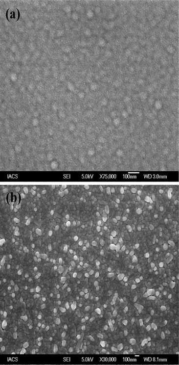 |
| | Fig. 1 FESEM image of (a) ZnS thin film deposited on ITO coated glass substrate and (b) ZnPc thin film deposited on the top of ZnS film. | |
The absorption spectra of ZnS and the ZnPc thin films deposited on ZnS at room temperature are shown in Fig. 2. The ZnS film shows an absorption peak nearly at 332 nm. The band gap energy was estimated to be 3.38 eV using the variation in absorption coefficient (α) with photon energy (hν). It has been mentioned in the previous article that the UV-vis absorption spectrum of metal phthalocyanines originates from the molecular orbitals within the aromatic 18-π electron system and from overlapping orbitals on the central metal.12 In the near UV region, the B-band or Soret band, representing the π → π* transition for the ZnPc film, shows a peak at ∼333 nm.12 The absorption band in the visible region with peak position in the range 623–696 nm is known as the Q-band (representing the π → π* transition), and has a doublet due to Davydov splitting.12,15 For ZnPc the intensity of the higher energy peak (∼623 nm) in the doublet is higher than that of the lower energy peak (∼696 nm). This behavior represents the typical features of the α-phase of a phthalocyanine.12 From optical absorption spectra, the band gap was determined by the peak energy at low energy maxima using the variation in absorption coefficient (α) with photon energy (hν).12 The estimated value of the energy gap for the as-prepared ZnPc film is 1.73 eV.
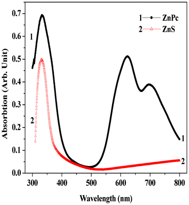 |
| | Fig. 2 UV-visible absorption spectra of ZnS and ZnPc thin films deposited on ZnS at room temperature (30 °C). | |
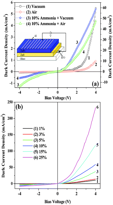 |
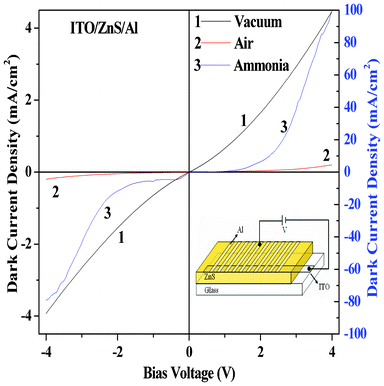
| | Fig. 3 Dark current–voltage characteristics of the heterojunction (ITO/ZnS/ZnPc/Al) devices in: (a) vacuum (curve 1), air (oxygen; curve 2), 10% aqueous ammonia plus vacuum (curve 3) and 10% aqueous ammonia plus air (curve 4). 1 and 2 refer to the left scale and 3 and 4 refer to the right scale. Inset shows the structure of a heterojunction device; (b) ammonia vapor (different concentrations of aqueous ammonia solution) at room temperature (30 °C). | |
We prepared organic–inorganic heterojunction devices based on n-type ZnS and p-type ZnPc as mentioned earlier. The I–V characteristics of these devices were determined under different ambient conditions such as in vacuum (10−3 torr), in air (i.e., in the presence of acceptor oxygen) and in the presence of donor gas NH3 containing water vapor (from aqueous solution of NH3). Such I–V characteristics in the case of vacuum (curve 1), air (oxygen) (curve 2), 10% aqueous ammonia plus vacuum (curve 3) and 10% aqueous ammonia plus air (curve 4) are shown in the Fig. 3(a). The current noted by the device in air (curve 2) decreases compared to vacuum (curve 1). Again, if ammonia is passed through the device kept in air, enhancement in current is observed as shown in curve 4. However, relatively higher current was noticed when ammonia was passed through the device kept in vacuum, as shown in curve 3, Fig. 3a. From Fig. 3a it is clear that if one introduces oxygen (air) instead of ammonia, decrease in current compared to the case of ammonia as well as vacuum is noticed. Thus the device is suitable for selectively sensing ammonia present in air or vacuum through current enhancement. Fig. 3(b) shows the I–V characteristics for ammonia environment of various concentrations. From Fig. 3(a) and (b) it is observed that after certain value (threshold voltage) of forward bias voltage, a sudden increase in current is noticed and the amount of increase depends on the surrounding environment. The I–V characteristics of the device ITO/ZnS/ZnPc/Al with ITO (work function of 4.8 eV) as the −ve electrode and Al (work function of 4.2 eV) as the +ve electrode have shown a typical p-n junction diode-like nature in all cases (Fig. 3). When the junction is forward biased (i.e., ZnPc in contact with the positive bias) and ZnS (in contact with the negative bias), a relatively large current can flow through the junction as shown in the Fig. 3. On the other hand, when a reverse bias is applied, only a small current can flow as the reverse bias increases barrier height.29Fig. 3(b) shows that the heterojunction device is highly sensitive to ammonia gas. The sensitivity of the heterojunction device for ammonia gas, of various concentrations, relative to air (i.e. the ratio of current (INH3) measured under ammonia environment to the current (Iair) measured under air) as a function of bias voltage is shown in Fig. 4(a). Similarly, the sensitivity of the heterojunction device for ammonia gas of various concentrations, relative to vacuum (i.e. the ratio of current measured (INH3) under ammonia environment to the current (Ivac) measured under vacuum) as a function of bias voltage is shown in Fig. 4(b). The sensitivity of the heterojunction device for air relative to vacuum (i.e. the ratio of current (Iair) measured in air to the current (Ivac) measured under vacuum, as a function of bias voltage is shown in Fig. 4(c). From Fig. 4 it is observed that the heterojunction device is highly sensitive to ammonia gas (and also air) at lower values of bias voltage. The variation of dark current density versus time for passing gas inside the conductivity chamber and after turning off the flow of gas (gas out) is shown in Fig. 5 (a) for ammonia gas of various concentrations. After turning off the flow of gas, the current returns to the original value in each case showing the reversibility of the process. However, for higher concentration of ammonia gas (Fig. 5(b)) the current takes longer time to attain original value of current noted before the gas was passed into the conductivity chamber. The values of rectification ratio (ratio of current at a certain value of forward bias to the corresponding value of current under same value of reverse bias) of the heterojunction diode under various environments were evaluated for different values of bias voltages. The evaluated values of the rectification ratio are shown in Table 1, which shows that the rectification ratio increases with bias voltage. The value of observed rectification ratio is comparable to the reported rectification ratios of organic materials.30 It should be mentioned here that the sensitivity of ammonia vapor for the current enhancement in the heterojunction device reported in the present experiment is much higher (about 800 times around 1.5 V) than that reported earlier by Muzikante et al.27 in the case of a heterojunction consisting of hexadecafluorinated nickel phthalocyanine (Ni(F16Pc)) and nickel phthalocyanine (NiPc). The plots of variation of response [(Iammonia − Iair)/Iair] and [(Iammonia − Ivac)/Ivac] versus aqueous ammonia concentration at 2V are shown in Fig. 6(a) and (b) respectively. Good linear plots with correlation factor R = 0.99 are obtained.
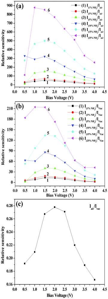 |
| | Fig. 4 Relative sensitivity of the heterojunction devices under different environments at room temperature (30 °C): (a) INH3/Iair, (b) INH3/Ivac and (c) Iair/Ivac. | |
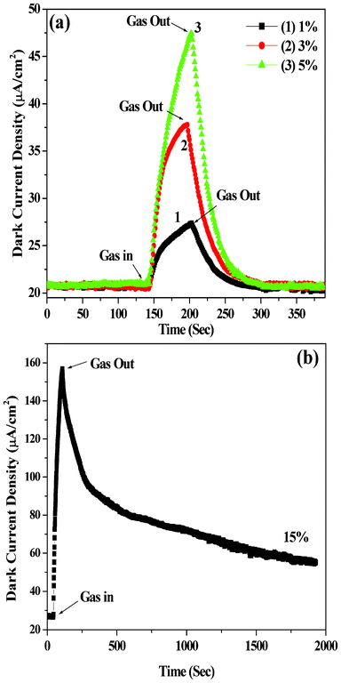 |
| | Fig. 5 Dark current-time characteristics for the heterojunction device (ITO/ZnS/ZnPc/Al) exposed to ammonia vapor: (a) 1, 3 and 5% and (b) 15% ammonia (from the aqueous ammonia solution). | |
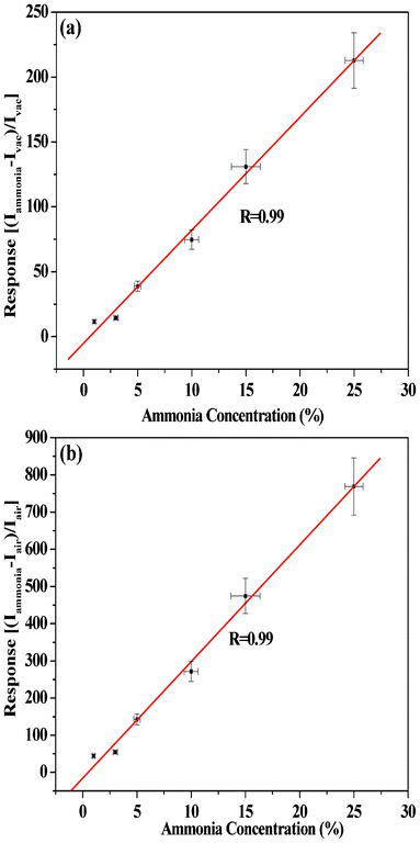 |
| | Fig. 6 Calibration curve representing the plot of response versus ammonia concentration with respect to (a) vacuum and (b) air for the device (ITO/ZnS/ZnPc/Al) at 2 V. Linear plots with correlation factor of R = 0.99 were obtained. | |
Table 1 Calculation of the rectification ratio (RR) of the heterojunction devices (ITO/ZnS/ZnPc/Al) under different environments (ammonia, air and vacuum).
| Voltage (Volt) |
Rectification ratio (RR) |
| Ammonia (%) |
Air |
Vacuum |
| 1 |
3 |
5 |
10 |
15 |
25 |
| 0.5 |
2.1 |
2.6 |
1.8 |
5.9 |
2.6 |
6 |
5.5 |
5.3 |
| 1 |
3.5 |
3.9 |
4.1 |
6.8 |
7.4 |
6.8 |
4.1 |
6.2 |
| 1.5 |
5.7 |
6.1 |
6.5 |
14.3 |
11.6 |
8.6 |
4.9 |
6.3 |
| 2 |
6.8 |
6.9 |
8.4 |
15.5 |
17.3 |
12.3 |
5.3 |
9.3 |
| 2.5 |
7.4 |
8.4 |
9.3 |
13.4 |
20.9 |
15.4 |
9.1 |
14.1 |
| 3 |
7.9 |
9.9 |
11 |
13.6 |
23.2 |
19.9 |
11.7 |
26.7 |
| 3.5 |
8.9 |
10.9 |
12.9 |
15.9 |
27.9 |
23.8 |
18.2 |
53.6 |
| 4 |
9.2 |
11.8 |
14 |
17.4 |
28.7 |
27.1 |
23.9 |
92 |
The effect of temperature on the I–V characteristics of the ITO/ZnS/ZnPc/Al device has also been studied in the temperature range (30–90 °C). Such I–V characteristics are shown in Fig. 7. From these I–V characteristics, good diode-like nature of the device is noticed in the studied temperature range. Diode current increases with temperature as expected for semiconducting materials and the threshold voltage also decreases with increasing temperature (as shown in the inset of Fig. 7). The high current flow at high temperatures may be either due to increased bond breaking, and thus generating more free charge carriers to participate in the conduction process, or due to increased de-trapping of the charge carriers from their respective trapping centers.2 The decrease in threshold voltage with increasing temperature is due to the possible reduction of the barrier height at higher temperatures. The values of the rectification ratio, measured at 4 V (above the threshold voltage), evaluated at 30, 50, 70 and 90 °C are 92, 42, 35 and 39, respectively. A decrease in rectification ratio was observed with the increase of temperature up to 70 °C. Such a decrease in rectification ratio could be due to fact that the reverse saturation current is more sensitive (compared to the value of the current at room temperature), up to a temperature of 70 °C than the forward current of the p-n junction diode.17 The increase in rectification ratio at 90 °C is due to the much greater enhancement in forward current (due to temperature induced enhancement in carrier density) compared to reverse current at this temperature.
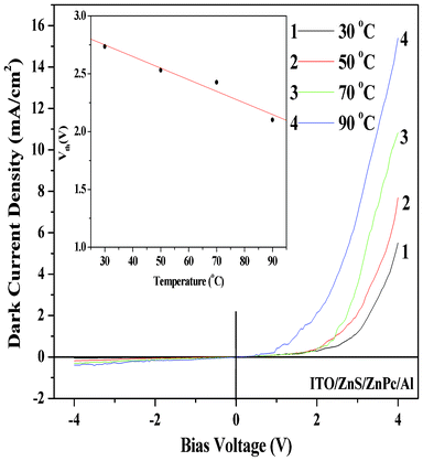 |
| | Fig. 7 Dark current–voltage characteristics (in vacuum) of the device (ITO/ZnS/ZnPc/Al) as a function of temperature. Inset shows the variation of threshold voltage (Vth) as a function of temperature. | |
As discussed earlier, the effect of donor gas (NH3 vapor from aqueous ammonia solution) and acceptor gas (O2) present in air on the current–voltage characteristics of the organic–inorganic (ITO/ZnS/ZnPc/Al) heterojunction diode was studied. Before studying the effect of gas adsorption on the heterojunction, the effect of gas adsorption on the I–V characteristics in the case of the single layer devices like ITO/ZnS/Al and ITO/ZnPc/Al were also studied as represented in Fig. 8 and Fig. 9, respectively. From the I–V characteristics of the single layer devices of ZnS (Fig. 8) and ZnPc (Fig. 9) in vacuum, diode-like rectification behaviour was not noticed. Experimental results reveals that there is some asymmetry in the I–V characteristics between the forward and reverse bias, which arises due to different work functions of the electrode material. Such types of current–voltage characteristics have also been observed previously for the heterojunction device consisting of Ni(F16Pc) and NiPc thin films sandwiched between Au and Al electrodes.27 In air, i.e. after exposure to acceptor gas O2, some free holes are created and consequently, a decrease in charge carrier (electron) density occurs in the n-type ZnS resulting in decrease in current.21 On the other hand after exposure of donor NH3 gas on n-type ZnS, the donor gas generates more free electrons inside the semiconductor material resulting in an increase of charge carrier density inside the ZnS layer and ultimately, an increase in the current for the single layer ZnS device was observed (Fig. 8).21 The reverse effect has been noticed (Fig. 9) in the case of the single layer ZnPc device on adsorption of donor and acceptor gases as ZnPc is a p-type semiconductor.31 When a donor type gas such as ammonia is adsorbed by p-type ZnPc material in film then ammonia produces donor states near the surface region of ZnPc which is fully compensated by the hole carriers of p-type ZnPc.6 Water vapor (present with NH3 as mentioned earlier) also acts as an effective donor even in the presence of a strong donor adsorbates such as ammonia.32 This causes a decrease in majority of the charge carriers, i.e. holes in the p-type ZnPc, resulting in the decrease in current as observed in the present experiment (Fig. 9). Twarowski proposed a model where he explained how oxygen molecules diffuse into the bulk of the ZnPc film and act as electron acceptor sites.33 It is also reported that the formation of charge-transfer complexes by the coordination of O2 to the metal center of MPc at the air/phthalocyanine interface leads to the formation of oxidized MPc+ and O2− species and injection of holes to the bulk solids takes place.4,34 Under open air, oxygen gas is coordinated with the metal atom of a phthalocyanine molecule through a charge transfer interaction to form a redox couple.35,36 The positive charge produced is then delocalized over Pc rings, can serve as a trap for electrons or donate holes to the sample. These acceptor gas-generated holes increase the charge carrier density in p-type ZnPc and that is why the highest current in ZnPc single layer devices was observed when measured in the presence of air (oxygen) as shown in Fig. 9. It should be mentioned here that the sensitivity of the single layer devices for both ammonia and air (i.e. oxygen) is much lower than that of the heterojunction device discussed above.
 |
| | Fig. 8 Shows the current–voltage characteristics, at room temperature (30 °C), of the device (ITO/ZnS/Al) under different atmospheres: (1) vacuum, (2) air and (3) ammonia. (1 and 2 correspond to left scale and 3 corresponds to right scale). Inset shows the device structure of ITO/ZnS/Al heterojunctions. | |
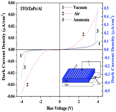 |
| | Fig. 9 Dark current–voltage characteristics, at room temperature (30 °C), of the device (ITO/ZnPc/Al) under different atmosphere: (1) vacuum, (2) air and (3) ammonia. (1 and 2 correspond to the left scale and 3 correspond to the right scale). Inset shows the device structure of the ITO/ZnPc/Al heterojunctions. | |
Electrical properties of heterojunction diode with device structure ITO/ZnS/ZnPc/Al was studied in the presence of NH3 and O2. I–V characteristics of such diode in the presence of O2 (air) and NH3 containing water vapor are shown in Fig. 3a and 3b, respectively. In the presence of donor NH3 gas containing water, the forward bias current increase dramatically with respect to the current in vacuum, while in the presence of acceptor O2 gas, forward current decreases with respect to the vacuum. This increase in forward current in the presence of donor gas and decrease in current in the presence of acceptor gas can be explained by both charge carrier generation due to the adsorbed gases and hence bending in energy bands of ZnPc in the presence of free carriers near the ZnPc/ZnS junction as discussed later. From the I–V curves of this ZnPc/ZnS heterojunction, we got a threshold voltage (Vth) of 2.72 V when measurements were done in vacuum, 2.76 V when measurements were done in air (i.e., in the presence of O2) and 1.55 V when measurements were done in the presence of NH3. This decrease in threshold voltage in the presence of donor gas and increase in threshold voltage in the presence of acceptor gas can also be explained by the band bending.37
As mentioned earlier the adsorption of donor ammonia gas decreases the hole density inside the ZnPc layer, when a forward bias is applied, a large number of electrons from the n-type ZnS layer move to the p-type ZnPc layer, out of which only a few electrons were captured by the lesser number of electron trapping centers, which remain after NH3 adsorption (recombination probability is very small or neglected) and may result in an increase in diode current. When O2 was absorbed by ZnPc, hole carrier density increases inside the ZnPc layer. In forward bias voltages the electron and holes diffuses through the junctions and the electrons when passing through the p-region might be trapped by the holes (high recombination probability), which may reduce the forward current with respect to other atmospheres. However, the very high forward current in the presence of donor NH3 gas and low current in the presence of O2 can be explained properly by the band bending at the ZnS and ZnPc interface. The work function of ZnPc (∼4.3 eV) is lower than that of ZnS (∼5.2 eV).37 It is suggested by Zhang et al.37 that the transfer of electrons from ZnPc to the ZnS layer is expected during interface formation, corresponding to a downward band bending in ZnS and upward band bending in ZnPc. They also mentioned37 that the formation of band bending may take place in both the ZnS substrate and the ZnPc film after the deposition of the film with 2.8 nm nominal thickness. But the applicability of band bending in organic semiconductors is unlikely due to the usual lower charge carrier concentration in these materials.37 In recent studies on the organic–organic heterojunction based on CuPc and F16CuPc, Wang et al.38 discussed that the accumulation of carriers during interface formation causes band bending at the organic–organic interface. ZnS is an n-type inorganic semiconductor with a larger charge carrier concentration as compared to charge carriers in ZnPc. But charge carriers inside the ZnPc layer can be tuned by the donor or acceptor vapor adsorption. So under doped condition sufficient numbers of charge carriers at the interface could be expected and that effectively bends the ZnPc band. It is reported that adsorption of different polar molecules may significantly change the surface band bending by modifying the surface state distribution.39 In the present case also the change in charge distribution in the surface states of ZnPc upon adsorption of vapors is possible, which may cause band bending. In our case the values of film thickness (100 nm) and the observed current values were much higher which indicates that the charge carrier concentration in the sample films is significant for causing band bending in our heterojunction devices. In the forward bias condition and in the absence of any gas, holes are injected to the ZnPc from the anode and electrons are injected to the ZnS from the cathode. These injected free holes and electrons move to the ZnPc/ZnS junction in the presence of applied electric field. If we consider the energy band diagram of these materials (before and after biasing, as shown in the Fig. 10(a) and Fig. 10(b), respectively), the highest occupied molecular orbital (HOMO) and lowest unoccupied molecular orbital (LUMO) levels of ZnPc are −5.2 eV and −3.5 eV, respectively,31 while valence band (EV) and conduction band (EC) energy of ZnS is −7.6 eV and −3.9 eV respectively.40 Since the EV of ZnS is 2.4 eV lower than the HOMO of ZnPc, holes within ZnPc are blocked by the ZnS layer and these accumulated holes bend the band of ZnPc as shown in the Fig. 10(b). ZnPc is the exposed surface in our case, so the carrier concentrations and position of the Fermi levels depends on the types of dopants.41–43Fig. 10(b) shows the position of the Fermi level of ZnPc under undoped conditions i.e. in the absence of any gases. It is reported that ZnPc is a P-type organic semiconductor and the equilibrium Fermi level (ΦZnPc) increases by 0.1–0.3 eV when the sample is exposed to oxygen due creation of holes inside the ZnPc layer.41–43 Whereas, the donor gas ammonia creates electron inside the ZnPc layer that decreases the Fermi level (ΦZnPc). So under doped conditions, the position of the Fermi level for the ZnS/ZnPc heterostructures is shifted to higher or lower energy due to exposure to O2 or ammonia vapor, respectively (figure not shown), as compared to undoped conditions. The LUMO level of ZnPc is slightly higher (0.4 eV) than the EC of ZnS and therefore electrons could move to the ZnPc layer from ZnS. However, this barrier for electron injection increases due to the bending of ZnPc band. When the diode is exposed in NH3 gas, NH3 diffusion takes place inside the ZnPc layer and creates some free electrons within the ZnPc layer as mentioned earlier. Water vapor could also create some electrons within the ZnPc layer. These free electrons recombine with the holes that are injected from the anode inside the ZnPc layer and reduce the accumulated hole density within the ZnPc layer near the ZnPc/ZnS junction, which reduces the band bending as shown in the Fig. 10(b) or band may not bend at all. From the Fig. 10(b), it is clear that the ZnPc band bends in such a way that if bending is less then the barrier height for electron injection from ZnS to ZnPc layer becomes smaller than the barrier height in vacuum and electron transport is favorable. As a result, electron injection efficiency from ZnS to the ZnPc layer increases very much which increases the forward current dramatically as shown in the Fig. 3(b) for ammonia gas. This decrease in barrier height due to the adsorption of donor NH3 gas also decreases the threshold voltage of the ZnS/ZnPc heterojunction dramatically from 2.72 V in vacuum to 1.55 V in the presence of NH3. On the other hand when the diode is exposed in open air (i.e., in O2), O2 diffusion to the ZnPc layer takes place which creates some free holes within the ZnPc layer as discussed earlier. This acceptor gas created holes along with the injected holes from the anode which greatly increases the free hole density within the ZnPc layer. Due to the application of forward bias these holes in the ZnPc layer move toward the ZnS layer and accumulate near the junction due to the deep EV of ZnS as mentioned earlier. These accumulated holes bend the ZnPc bands heavily near the junction, increasing the electron injection barrier. Therefore the electron injection efficiency from the ZnS to ZnPc is drastically reduced, which results in a very low forward current (lowest in the present experiment among the three studied environments). This increase in barrier height due to the adsorption of acceptor gas O2 also increases the threshold voltage of the ZnS/ZnPc heterojunction from 2.72 V in vacuum to 2.76 V in the presence of O2. It is very difficult to measure the band bending quantitatively due to gas adsorption on the heterojunction devices. The change in current and threshold voltage of the ITO/ZnS/ZnPc/Al heterojunction suggests that this diode could be a potential candidate for sensing/detecting gas, especially donor gas NH3.
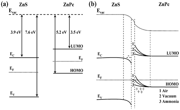 |
| | Fig. 10 (a) Schematic energy band diagram of ZnS and ZnPc before and (b) after the contact (under different environments: (1) air, (2) Vacuum and (3) Ammonia). Evac and EF denote the vacuum level and the Fermi level (undoped conditions), respectively. Position of EF increases (air) or decreases (ammonia) under doped conditions (not shown in figure). | |
4. Conclusions
Current–voltage (I–V) characteristics of the heterojunction devices ITO/ZnS/ZnPc/Al, using nanostructured films of ZnS and ZnPc, have shown diode-like characteristics under different environments. In contrast, the single layer devices like ITO/ZnS/Al and ITO/ZnPc/Al have not shown such diode-like behaviour. An increase in current in the n-type ZnS single layer device was observed when the device was exposed in donor gas aqueous NH3, while a decrease in current was noticed when the device was exposed to air (acceptor gas O2). Current in the heterojunction device, especially in the forward direction, increased more than 200 times compared to vacuum and more than 800 times compared to air in 1.5 volt bias. The threshold voltage decreased significantly when the heterojunction device was exposed to the donor gas NH3. On the other hand, a decrease in device current with an increase in threshold voltage has been noticed when the diode was exposed to air. This increase in current in the presence of NH3 and a decrease in current in the presence of O2 have been explained by the creation of charge carriers inside the ZnPc layer in the presence of gases and hence bending of ZnPc band near the ZnS/ZnPc junction. The decrease in threshold voltage in the presence of donor gas NH3 and increase in threshold voltage in the presence of acceptor gas O2 adds further support in favor of band bending in the ZnPc layer. Excellent reversibility of the heterojunction devices has been observed when exposed to lower concentrations of ammonia gas. The change in current values and threshold voltages in the presence of gases suggests that this heterojunction device could be a potential candidate for sensing gases, especially for sensing NH3 gas.
Acknowledgements
One of the authors, Bipul Biswas thanks the Council of Scientific and Industrial Research (CSIR), New Delhi, India, for providing financial assassistance the form of NET CSIR fellowship (File No.: 09/080 (0628)/2008/EMR-I).
References
- D. Li, E. J. Borkent, R. Nortrup, H. Moon, H. Katz and Z. Bao, Appl. Phys. Lett., 2005, 86, 042105 CrossRef.
- M. M. Ahmed, K. S. Karimov and S. A. Moiz, IEEE Trans. Electron Devices, 2004, 51, 121 CrossRef CAS.
- P. S. Smertenko, V. P. Kostylev, V. V. Kislyuk, A. F. Syngaevsky, S. A. Zynio and O. P. Dimitriev, Sol. Energy Mater. Sol. Cells, 2008, 92, 976 CrossRef CAS.
- F. I. Bohrer, A. Sharoni, C. Colesniuc, J. Park, I. K. Schuller, A. C. Kummel and W. C. Trogler, J. Am. Chem. Soc., 2007, 129, 5640 CrossRef CAS.
- Q. Zhou and R. D Gould, Thin Solid Films, 1998, 317, 432 CrossRef CAS.
- M. Bouvet, V. Parra, C. Locatelli and H. Xiong, J. Porphyrins Phthalocyanines, 2009, 13, 84 CrossRef CAS.
- B. J. Prince, B. E. Williamson and R. J. Reeves, J. Lumin., 2001, 93, 293 CrossRef CAS.
- A. O. Ribeiro, J. C. Biazzotto and O. A. Serra, J. Non-Cryst. Solids, 2000, 273, 198 CrossRef CAS.
- G. L. Pakhomov, G. P. Shaposhnikov, V. N. Spektor, L. G. Pakhomov and J. M. Ribo, Russ. Chem. Bull., 1996, 45, 228 CrossRef.
- B. Schöllhorn, J. P. Germain, A. Pauly, C. Maleysson and J. P. Blanc, Thin Solid Films, 1998, 326, 245 CrossRef.
- S. Karan, D. Basak and B. Mallik, Chem. Phys. Lett., 2007, 434, 265 CrossRef CAS.
- S. Karan and B. Mallik, J. Phys. Chem. C, 2007, 111, 7352 CAS.
-
B. Mallik and S. Karan, Modern Research and Educational Topics in Microscopy, 2007, A. Méndez-Vilas and J. Díaz (ed.), Formatex, 671 Search PubMed.
- S. Karan and B. Mallik, J. Phys. Chem. C, 2008, 112, 2436 CAS.
- A. Chowdhury, B. Biswas, M. Majumder, M. K. Sanyal and B. Mallik, Thin Solid Films, 2012, 520, 6695 CrossRef CAS.
- S. Karan and B. Mallik, Nanotechnology, 2008, 19, 495202 CrossRef.
- S. Karan and B. Mallik, Phys. Chem. Chem. Phys., 2008, 10, 6751 RSC.
- S. Karan, D. Basak and B. Mallik, Curr. Appl. Phys., 2010, 10, 1117 CrossRef.
- S. Karan and B. Mallik, Thin Solid Films, 2012, 520, 2343 CrossRef CAS.
- S. S. Mali, D. S. Dalavi, P. N. Bhosale, C. A. Betty, A. K. Chauhan and P. S. Patil, RSC Adv., 2012, 2, 2100 RSC.
- L. Xu, H. Song, T. Zhang, H. Fan, L. Fan, Y. Wang, B. Dong and X. Bai, J. Nanosci. Nanotechnol., 2011, 11, 2121 CrossRef CAS.
- S. V. Pol, V. G. Pol, J. M. Calderon-Moreno, S. Cheylan and A. Gedanken, Langmuir, 2008, 24, 10462 CrossRef CAS.
- J. Lahiri and M. Batzill, J. Phys. Chem. C, 2008, 112, 4304 CAS.
- M. E. Azim-Araghi and A. Krier, Appl. Surf. Sci., 1997, 119, 260 CrossRef CAS.
- V. V. Cherpak, P. Y. Stakhira, O. I. Kuntyy and A. Zakutayev, Mol. Cryst. Liq.
Cryst., 2008, 496, 131 CrossRef CAS.
- G. L. Pakhomov, L. G. Pakhomov, V. V. Travkin, M. V. Abanin, P. Y. Stakhira and V. V. Cherpak, J. Mater. Sci., 2010, 45, 1854 CrossRef CAS.
- I. Muzikante, V. Parra, R. Dobulans, E. Fonavs, J. Latvels and M. Bouvet, Sensors, 2007, 7, 2984 CrossRef CAS.
- R. N. Bera and B. Mallik, Synth. Met., 1999, 99, 61 CrossRef CAS.
- X. Duan, Y. Huang, Y. Cui, J. Wang and C. M. Lieber, Nature, 2001, 409, 66 CrossRef CAS.
- G. J. Ashwell, J. Ewington and B. J. Robinson, Chem. Commun., 2006, 618 RSC.
- Z. R. Hong, R. Lessmann, B. Maennig, Q. Huang, K. Harada, M. Riede and K. Leo, J. Appl. Phys., 2009, 106, 064511 CrossRef.
- A. Belghachi and R. A. Collins, J. Phys. D: Appl. Phys., 1990, 23, 223 CrossRef CAS.
- A. Twarowski, J. Chem. Phys., 1982, 77, 5840 CrossRef CAS.
- H. R. Kerp, K. T. Westerdui, A. T. van Veen and E. E. van Faassen, J. Mater. Res., 2001, 16, 503 CrossRef CAS.
- G. L. Pakhomov, L. G. Pakhomov and V. N. Spektor, Russ. Chem. Bull., 1995, 44, 1432 CrossRef.
- H. Y. Wang and J. B. Lando, Langmuir, 1994, 10, 790 CrossRef CAS.
- L. Zhang, H. Peisert, I. Biswas, M. Knupfer, D. Batchelor and T. Chasse, Surf. Sci., 2005, 596, 98 CrossRef CAS.
- H. Wang, J. Wang, H. Huang, X. Yan and D. Yan, Org. Electron., 2006, 7, 369 CrossRef CAS.
- E. Capua, A. Natan, L. Kronik and R. Naaman, ACS Appl. Mater. Interfaces, 2009, 11, 2679 Search PubMed.
- S. Kundu and L. C. Olsen, Thin Solid Films, 2005, 471, 298 CrossRef CAS.
- M. Pfeiffer, K. Leo and N. Karl, J. Appl. Phys., 1996, 80, 6880 CrossRef CAS.
- W. Gao and A. Kahn, Org. Electron., 2002, 3, 53 CrossRef CAS.
- J. Blochwitz, T. Fritz, M. Pfeiffer, K. Leo, D.M. Alloway, P. A. Lee and N. R. Armstrong, Org. Electron., 2001, 2, 97 CrossRef CAS.
Footnote |
| † Permanent address: Basirhat College, Basirhat, North 24 Parganas-743412 |
|
| This journal is © The Royal Society of Chemistry 2012 |
Click here to see how this site uses Cookies. View our privacy policy here.