Realization of transparent and flexible capacitors using reliable graphene electrodes†
Sin-Hye
Na‡
a,
Hyun-A
Song‡
a and
Soon-Gil
Yoon
*ab
aDepartment of Materials Engineering, Chungnam National University, Daeduk Science Town, 305-764, Daejeon, Korea
bGraduate of Analytical Science and Technology, Chungnam National University, Daeduk Science Town, 305-764, Daejeon, Korea. E-mail: sgyoon@cnu.ac.kr
First published on 29th March 2012
Abstract
Reliable graphenes grown by rapid-thermal pulse chemical vapor deposition (CVD) for electrode applications were selectively patterned under optimum conditions for argon rf plasma power and etching time. For the transparent and the flexible capacitors using Bi2Mg2/3Nb4/3O7 (BMNO) dielectric films grown at room temperature, the graphene top and bottom electrodes were integrated onto the polymer substrates. The graphene/BMNO/graphene/Ti/polyethersulfone (PES) capacitors showed typical dielectric and leakage properties for capacitors. The adhesion between substrates and the graphene should be critically considered in order to improve the leakage properties of the capacitors. Graphene that possessed a high bendability was the predominant candidate for application to the top and bottom electrodes of the transparent and flexible capacitors.
Introduction
Graphene has attracted significant attention due to its outstanding properties, which render it a suitable candidate material for electronics applications.1–6 Existing routes for graphene synthesis include mechanical or chemical cleavage of graphite,7–9 bottom-up approaches by chemical synthesis,10 and epitaxial growth methods on silicon carbide11,12 or on metal substrates.13–15 To date, the CVD process is known to be the most powerful method for large-area graphene synthesis. Graphene was segregated from the transition metal surface under working pressure by dissolving carbon in metal at high temperatures followed by cooling at various rates. However, with respect to graphene growth by CVD, reproducibility of the graphene growth remained among the first of the problems to be solved. That is, the hydrocarbon (CH4) that remained in the growing chamber after the graphene experiment contributed to subsequent graphene growth, although the growing chamber was completely evacuated after graphene growth. When that is the case, it presents an important problem for the reliable growth of the graphene. The second problem of graphene growth using CVD was the required amount of time—above 5 h.16,17 The extended amount of time presents a disadvantage for mass production in industry. In order to reduce the synthesis time of the graphene, rapid-thermal pulse CVD was used in the present study.Bendable electrodes are required for embedment of the dielectric materials onto a flexible polymer substrate, and they should be appropriately patterned for top and bottom electrode applications. For application onto flexible substrates, bendability of the electrodes is a critical element. Al-doped ZnO (AZO), indium–gallium doped ZnO (IGZO), and indium–tin oxide (ITO), which are frequently used for transparent electrodes, have bendabilities of approximately 0.03, 0.3, and 0.58–1.15%, respectively. However, the bendability of the graphene was approximately 15–20%, which was significantly higher.
Capacitor applications that use thin films require a low leakage current density and a high dielectric permittivity. If thin film capacitors must be integrated onto flexible substrates, high-dielectric-permittivity oxide films must be grown at room temperature. To obtain a high dielectric permittivity in amorphous films, BMNO dielectric materials with a pyrochlore structure were chosen, as they have a dielectric permittivity of about 210 for crystallized bulk material.18 In the case of thin films, 200 nm-thick BMNO films deposited at room temperature showed a low leakage current density of about 10−8 A cm–2 at 3 V and a dielectric permittivity of about 45 at 100 kHz.19,20
Graphene was synthesized using rapid-thermal pulse CVD to decrease the synthesis time and induce reproducible growth. Graphene for top electrode applications was patterned using argon plasma with different rf powers and etching times for electrode applications of the capacitors. The amorphous BMNO films were grown onto the graphene bottom electrode at room temperature using pulsed laser deposition and were characterized with respect to dielectric and leakage current properties using a graphene (top electrode)/BMNO/graphene (bottom electrode)/PES capacitor structure for transparent and flexible capacitor applications.
Experimental section
Graphene was grown onto 250 nm-thick Ni films/Si (001) using a rapid-thermal pulse chemical vapor deposition technique. Deposition conditions and the working pressure at each step were plotted and are explained in detail in Fig. S1 (ESI†). The synthesis of the graphene was performed for about 16 min, which includes the growth time of the graphene (30 s). The graphene was investigated using Raman spectroscopy (JY LabRam HR) with an Ar ion laser (514.53 nm wavelength) at 0.5 mW. Morphologies of the graphene transferred onto the glass were observed using atomic force microscopy (AFM) and an optical microscope. Etching of the nickel substrate layers and then transferring isolate graphene to the other substrates was performed using an aqueous iron chloride (1 M FeCl3) solution. The resistance and the mobility of the graphene were measured using the Hall system (Accent HL5500) with a magnetic field of 0.514 Tesla and a target Vr of 20 mV. The measurement conditions included a current of 0.123 mA DC and a voltage of 0.17 V. The optical properties were measured at room temperature with an HP 8453 UV/Visible spectrophotometer after transferring the floating graphene to glass or polymer plates. The graphene patterning was performed using a diode-type rf plasma in an argon ambient at room temperature. For the graphene top electrode of the dielectric materials, silver 100 μm in diameter used a shadow mask and was deposited onto the transferred graphene on the BMNO dielectric film, followed by etching using argon plasma. Finally, the silver that remained after the etching was removed by dissolution from a solution including iodine because silver reacts readily with iodine at room temperature, resulting in an AgI solution. For the transparent capacitor, we used 700 μm-thick glass and 300 μm-thick PES, respectively, as substrates. For capacitor applications, high dielectric constant BMNO thin films were deposited at room temperature using pulsed laser deposition (PLD) onto the graphene bottom electrode. In order to enhance the adhesion between the graphene bottom electrode and glass (or PES) substrate, a 3 nm-thick Ti layer was deposited onto the glass substrate at room temperature using dc sputtering. The dielectric properties of the 200 nm-thick BMNO thin films were evaluated at 100 kHz using an impedance gain phase analyzer (HP 4194A). The leakage current characteristics of the BMNO capacitors were investigated via HP4145B semiconductor parameter analysis. A bending test of the BMNO films grown onto Pt, ITO, and a graphene bottom electrode was performed by the method shown in the inset of Fig. 4(d). One side of a 1 × 1 cm2 sample was fixed and the other side was pushed. The samples bent at each point were maintained for 30 s. The surface images of the samples after bending at each point were measured by atomic force microscopy (AFM) using an optical microscope.Results and discussion
1. Reproducible graphene growth using rapid-thermal pulse CVD
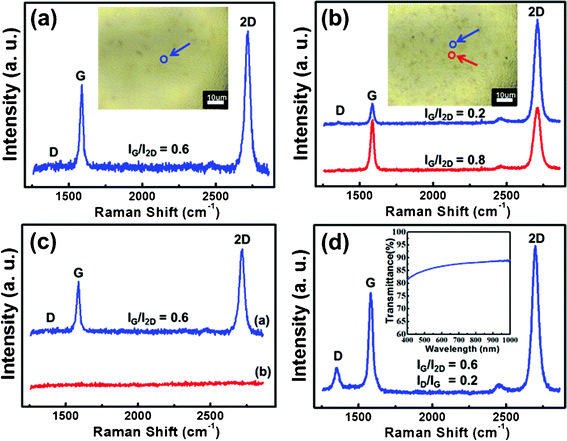
Fig. 1(a), and the inset of 1(a), shows the Raman spectroscopy (with excitation wavelength at 514 nm) and image, respectively, of the graphene as-deposited at 900 °C for 30 s in reaction gas mixtures (CH4![[thin space (1/6-em)]](https://www.rsc.org/images/entities/char_2009.gif) :H2 = 1:5 sccm). From the Raman spectroscopy observed in the circle of the image, a G band of ∼1580 cm−1 and a G' (2D) band of ∼2700 cm−1 were clearly observed and the absence of a D peak (∼1360 cm−1) corresponded to a very low defect density. A single Lorentzian profile of the 2D band corresponded to the hallmarks of a monolayer graphene.21 In these results, ID/IG = 0.05, which exhibited a very low defect density in the films, was also observed away from the graphene edges, suggesting the existence of sub-domain boundaries in areas with a constant number of graphene layers.22 In order to investigate whether the graphene grows when the CH4 is stopped after the growth of graphene using CH4, experiments without CH4 at 900 °C for 300 s in N2 (100 sccm) and H2 (50 sccm) ambient were performed. Fig. 1(b), and the inset of 1(b), shows the Raman spectroscopy and image of the graphene films observed after 4 consecutive experiments under the same conditions without the insertion of a CH4 source. The results in Fig. 1(b) were measured at the circles of the image in the inset. After several experiments without CH4, the deposition of the graphene was clearly observed, as shown in Fig. 1(b). This result suggests that the CH4 still existed in the growing chamber although the reactor was evacuated for a long time after graphene growth, and the remaining CH4 exerted a great influence on the reproducible graphene growth. For reproducible graphene growth, the residual CH4 should be completely removed from the growing chamber for subsequent graphene growth. Fig. 1(c) shows the Raman spectrums of the graphene grown with and without CH4. Compared with the results of the graphene grown in the presence of CH4 ((a) in Fig. 1(c)), (b) in Fig. 1(c) shows the Raman results of the graphene grown in the absence of CH4 (by an insertion of H2 only) after an annealing treatment in oxygen ambient. The oxygen treatment at 700 °C for 30 min in the absence of CH4 exhibited the complete removal of the graphene. The graphene growth was followed by a thermal treatment at 700 °C for 30 min in oxygen without an insertion of CH4.
:H2 = 1:5 sccm). From the Raman spectroscopy observed in the circle of the image, a G band of ∼1580 cm−1 and a G' (2D) band of ∼2700 cm−1 were clearly observed and the absence of a D peak (∼1360 cm−1) corresponded to a very low defect density. A single Lorentzian profile of the 2D band corresponded to the hallmarks of a monolayer graphene.21 In these results, ID/IG = 0.05, which exhibited a very low defect density in the films, was also observed away from the graphene edges, suggesting the existence of sub-domain boundaries in areas with a constant number of graphene layers.22 In order to investigate whether the graphene grows when the CH4 is stopped after the growth of graphene using CH4, experiments without CH4 at 900 °C for 300 s in N2 (100 sccm) and H2 (50 sccm) ambient were performed. Fig. 1(b), and the inset of 1(b), shows the Raman spectroscopy and image of the graphene films observed after 4 consecutive experiments under the same conditions without the insertion of a CH4 source. The results in Fig. 1(b) were measured at the circles of the image in the inset. After several experiments without CH4, the deposition of the graphene was clearly observed, as shown in Fig. 1(b). This result suggests that the CH4 still existed in the growing chamber although the reactor was evacuated for a long time after graphene growth, and the remaining CH4 exerted a great influence on the reproducible graphene growth. For reproducible graphene growth, the residual CH4 should be completely removed from the growing chamber for subsequent graphene growth. Fig. 1(c) shows the Raman spectrums of the graphene grown with and without CH4. Compared with the results of the graphene grown in the presence of CH4 ((a) in Fig. 1(c)), (b) in Fig. 1(c) shows the Raman results of the graphene grown in the absence of CH4 (by an insertion of H2 only) after an annealing treatment in oxygen ambient. The oxygen treatment at 700 °C for 30 min in the absence of CH4 exhibited the complete removal of the graphene. The graphene growth was followed by a thermal treatment at 700 °C for 30 min in oxygen without an insertion of CH4.
 | ||
| Fig. 1 (a) Raman spectroscopy and image (inset) of the graphene films as-deposited at 900 °C for 30 s in reaction gas mixtures (CH4:H2 = 1:5 sccm). (b) Raman spectroscopy and image (inset) of the graphene films observed after four consecutive experiments under the same conditions without the insertion of a CH4 source. (c) Raman spectra of the graphene grown with (a) CH4 and without (b) CH4 (by an insertion of H2 only) after thermal annealing at 700 °C for 30 min in an oxygen atmosphere. (d) Raman spectrum of the graphene transferred to the SiO2/Si substrate, and (inset) transmittance of the graphene transferred to the glass substrate. | ||
In order to evaluate the properties of the graphene, they were transferred to the glass and the SiO2/Si substrates after the etching of the metals.22–24Fig. 1(d) shows the Raman spectrum of the graphene transferred to the SiO2/Si substrate and indicates that IG/I2D = 0.6 and ID/IG = 0.2, which still showed a monolayer of graphene. The inset of Fig. 1(d) shows the transmittance of the graphene transferred to the glass substrate as a function of the wavelength. The transmittance of the graphene was approximately 86% at a wavelength of 550 nm. The sheet resistance and the mobility of the graphene were about 513 Ω sq−1 and 2.8 × 103 cm2 V–1 s, respectively, from the Hall measurement at 0.123 mA and 0.17 V. This result was consistent with the results reported by Lee et al.25
AFM and optical images of the graphenes etched for different argon plasma powers for 30 min and for different times at an argon plasma power of 50 W are described in detail in Fig. S2 and S3 (ESI†), respectively. The etching results suggest that the graphenes were completely removed at an argon rf plasma power of 50 W and with an etching time of 60 min. The etching results show that the graphene was selectively etched for electrode applications for a transparent and flexible capacitor.
Fig. 2(a) shows the optical microscopy of the graphene patterned for 60 min at an rf power of 50 W using photolithography. From the image, graphenes 100 and 200 μm in diameter were clearly patterned by argon plasma. In order to clearly observe the patterning of the graphene, the Raman spectra observed at the non-etched and the etched areas are shown in Fig. 2(b) and 2(c), respectively. The insets of Fig. 2(b) and 2(c) show the Raman image observed at the non-etched and the etched areas, respectively. The non-etched area exclusive of the circles showed a Raman spectrum indicating some remaining graphene (see Fig. 2(b)), while the etched area (circles) showed no spectrum indicating graphene (see Fig. 2(c)). That result suggested that the graphene was completely patterned by the diode-type argon plasma. Generally, a shadow mask was conveniently used to define clearly the top electrode of the dielectric materials. The patterned graphene for the top electrode is shown in Fig. 2(d). The Raman spectra for the non-etched and the etched areas are shown in Fig. 2(e) and 2(f), respectively. As shown in Fig. 2(e), the circles patterned for the top electrode clearly showed a mono-layer graphene, while no graphene was observed at the regions exclusive of the circles, as shown in Fig. 2(f).
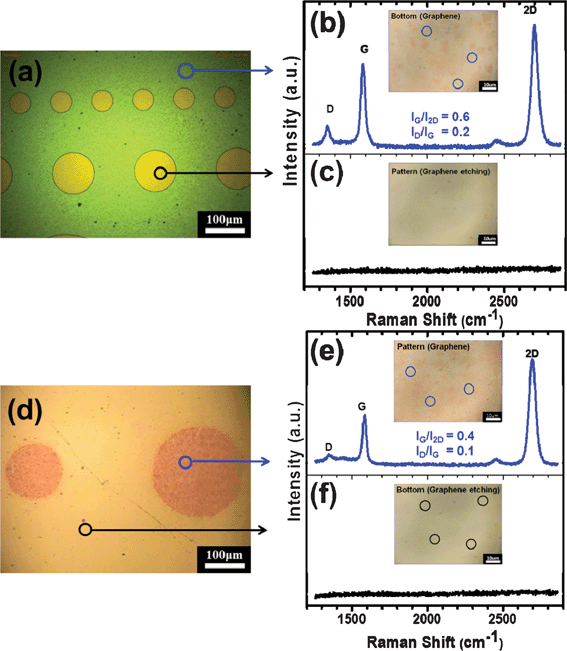 | ||
| Fig. 2 (a) Optical microscopy of the graphene patterned for 60 min at an rf power of 50 W using photolithography with different diameters. Raman spectra observed for (b) the non-etched and (c) the etched areas. Inset of each figure shows the Raman image of the non-etched and the etched areas. (d) Optical microscopy of the graphene patterned for the top electrode. Raman spectra observed for (e) the non-etched and (f) the etched areas. Silver was deposited using a shadow mask by dc sputtering and, after plasma etching, the silver was removed using a solution that included iodine. Inset of each figure shows the Raman images of the non-etched and the etched areas. | ||
2. Electrode applications of the graphene for transparent and flexible capacitors
Graphene (top electrode)/BMNO/graphene (bottom electrode)/Ti (3 nm)/glass or PES (MIM) structures were considered for transparent and flexible capacitor applications using graphene electrodes. Fig. 3(a) shows the transmittance of the MIM structures integrated onto the glass and PES substrates. Transmittances of the different structures were standardized by a transmittance of the Ti/glass and Ti/PES. An integration of the additional layers gradually decreased the transmittance of the structure. Transmittances (wavelength of 550 nm) of the Ti (3 nm)/glass, graphene/Ti/glass, BMNO/graphene/Ti/glass, and graphene/BMNO/graphene/Ti/glass were approximately 95, 86, 77, and 72%, respectively. However, transmittances of the Ti (3 nm)/PES and graphene/BMNO/graphene/Ti/PES were about 86 and 68%, respectively, at a wavelength of 550 nm. An AFM image of the graphene/BMNO/graphene/Ti/glass is shown in Fig. S4 (ESI†). The graphene transferred onto the BMNO/graphene/Ti/glass showed a severe wrinkle, resulting in a transmittance that was lower than that of the BMNO/graphene/Ti/glass. From the results of the transmittance, the transmittance of the MIM structure for the transparent capacitor applications was determined by that of the graphene, indicating that the graphene must be of good quality.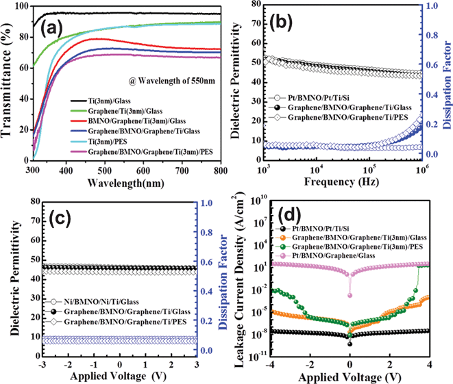 | ||
| Fig. 3 (a) Transmittance of the different structures integrated onto the glass and PES substrates. (b) Dielectric permittivity and dissipation factor as a function of frequency. (c) Dielectric permittivity vs. applied voltage at 100 kHz for various structures. (d) Leakage current characteristics of the Pt/BMNO/Pt/Ti/Si, Pt/BMNO/graphene/glass, graphene/BMNO/graphene/Ti (3 nm)/glass, graphene/BMNO/graphene/Ti (3 nm)/PES as a function of the applied voltage. | ||
In the present study, the Pt top (100 μm diameter) and bottom electrodes were used to compare the electrical properties of the graphene (100 μm diameter)/BMNO (200 nm)/graphene grown onto Ti/glass and Ti/PES substrates. Fig. 3(b) shows variations in the dielectric permittivity and the dissipation factor (dielectric loss) of Pt/BMNO/Pt/Ti/glass, graphene/BMNO/graphene/Ti/glass, and graphene/BMNO/graphene/Ti/PES capacitors as a function of frequency. The dielectric permittivity showed typical characteristics exhibiting a few dispersions with increasing frequency. Compared with the Pt electrode, the dissipation factor of the films grown onto the graphene increased at 2 × 10⁵ Hz, which was attributed to the resistivity (∼10−4 Ω cm) of the graphene. The oxide electrodes such as indium-doped Al-doped ZnO (AIZO),26 LaNiO3,27 and La0.5Sr0.5CoO3(LSCO)28 increased the dielectric loss of the capacitors by a higher resistivity (above 10−4 Ω cm) than that of the metals (ρ = 1–10 μΩ cm in the case of Pt, Au etc.).20 In the same manner, the graphene electrode (ρ = ∼10−4 Ω cm) increased the total dielectric loss of the capacitor at a high frequency of about 105 Hz. Dielectric permittivity and the dielectric loss were approximately 46 and 5%, respectively, at 100 kHz. Fig. 3(c) shows the relationship between dielectric permittivity and an applied voltage at a frequency of 100 kHz. The dielectric permittivity and the dielectric loss showed typical para-electric properties without a hysteresis of the BMNO dielectrics at an applied voltage of ±3 V. This result was consistent with that of the 200 nm thick BMNO films grown onto Pt and Cu bottom electrodes by PLD.20Fig. 3(d) shows the leakage current characteristics of the Pt/BMNO/Pt/Ti/glass, Pt/BMNO/graphene/glass, graphene/BMNO/graphene/Ti/glass, and graphene/BMNO/graphene/Ti/PES capacitors as a function of applied voltage. The Pt/BMNO/graphene/glass capacitor, without a Ti adhesion layer, showed a very high leakage current density (about 1 A cm–2) in the range of an applied voltage of ±2 V. However, graphene/BMNO/graphene/Ti/glass capacitors showed an improved leakage property of about 8 μA cm–2 at ±2 V, indicating the importance of the adhesion between the graphene and the glass substrate. The graphene/BMNO/graphene/Ti/PES capacitors also showed improved leakage properties. In the Pt/BMNO/graphene/glass structure without a Ti layer, BMNO/graphene was completely detached from the glass substrate through the adhesive tape test. From the results of the adhesive tape test, the adhesion between the BMNO and the graphene was satisfactory for the electrode applications of the graphene. Leakage properties of the BMNO were governed by Schottky emission, indicating an interface effect between the BMNO and the electrodes.29 The Schottky emitted mechanism was only limited when the electrode was strongly bonded to the substrate. The adhesion of the bottom electrode deposited onto the substrate influenced the leakage properties of the dielectric films, because the strong adhesion between the bottom electrode and the substrate also improved the interface state between the dielectric film and the bottom electrode. Therefore, the adhesion of the substrates contacting the graphene is critical in order to improve the leakage properties of the capacitors. As the results of the present study show, it is possible to apply graphene to top and bottom electrodes of transparent capacitors.
Bendability of the various electrodes grown onto a flexible substrate was required for application to a flexible capacitor. In the present study, BMNO/Pt/Ti/PES, BMNO/ITO/Ti/PES, BMNO/graphene/Ti/PES, and BMNO/Cu/Ti/PES samples were used for the bending test. The bending experiment was performed by the method shown in the inset of Fig. 4(d), and the method is described in detail in the experimental section. Fig. 4(a), 4(b) and 4(c) show the AFM images of the BMNO surface after bending for 30 s at 4 mm (3 (green line) in the inset of Fig. 4(d)) for BMNO/Pt, BMNO/ITO, and BMNO/graphene, respectively. The insets in each figure show optical images indicating a clear crack formation in the BMNO films grown onto different bottom electrodes. From the AFM and optical images, BMNO films grown onto Pt and ITO included severe cracks after bending, while BMNO films grown onto graphene maintained a smooth surface after bending, as shown in Fig. 4(c). In the present study, BMNO films grown onto a Cu electrode (not shown here) showed cracks similar to those of Pt and ITO electrodes. The rms (root mean square) roughness of the BMNO films grown onto different bottom electrodes is shown in Fig. 4(d) for bending distance. The surface roughness of the BMNO films grown onto Pt, Cu, and ITO electrodes increased in a linear fashion as bending distance increased, while the surface roughness of the BMNO films grown onto graphene was maintained without a typical change of the BMNO films as the bending distance was increased. In the case of the Pt and Cu bottom electrodes, rms roughness of the BMNO films bent at 6 mm was not indicated because the films included many cracks that we were not able to measure using AFM. In order to investigate the device performance of the graphene/BMNO/graphene/Ti/PES after the bending, leakage properties, which are the most sensitive to the bending, were plotted in Fig. 4(e) before and after the bending at 0.6 cm for 30 s. After a severe bending, leakage current density was not typically changed, compared with that of the sample before the bending. From the results of the microstructure and the electrical properties after the bending, graphene was concluded to be a suitable electrode for flexible capacitors.
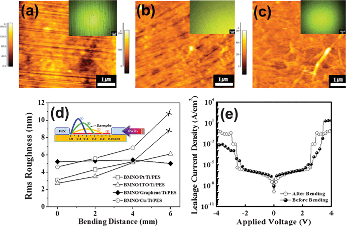 | ||
| Fig. 4 AFM images of the BMNO surface after bending for 30 s at 4 mm (3 (green line) in the inset of Fig. 4(d)) for (a) Pt, (b) ITO, and (c) grapheme-bottom electrodes. Insets in each figure show an optical image indicating a clear crack formation in the BMNO films grown onto different bottom electrodes. (d) Variations in the rms (root mean square) roughness for the bending distance using various samples. (e) Leakage current density vs. applied voltage of graphene/BMNO/graphene/Ti/PES sample before and after bending at 0.6 cm for 30 s. | ||
Conclusions
Reliable graphenes grown by rapid-thermal pulse CVD were selectively patterned under optimum conditions of argon rf plasma power and etching time for electrode applications. The present study established the possibility for graphene top and bottom electrode application to transparent and flexible capacitors using BMNO dielectric films. The graphene/BMNO/graphene/Ti/glass (or PES) capacitors showed typical dielectric and leakage properties of BMNO capacitors. The adhesion between substrates and the graphene is critical in order to improve the leakage properties of the capacitors. The high degree of bendability for graphene was a breakthrough in its application as top and bottom electrodes for transparent and flexible capacitors.Acknowledgements
This work was funded by the Ministry of the Economy, Science and Technology (MEST) (No. 2011-0000359).References
- F. Schedin, A. K. Geim, S. V. Morozov, E. W. Hill, P. Blake, M. I. Katsnelson and K. S. Novoselov, Nat. Mater., 2007, 6, 652 CrossRef CAS.
- J. B. Oostinga, H. B. Heersche, X. Liu, A. F. Morpurgo and L. M. K. Vandersypen, Nat. Mater., 2008, 7, 151 CrossRef CAS.
- T. Ohta, A. Bostwick, T. Seyller, K. Horn and E. Rotenberg, Science, 2006, 313, 951 CrossRef CAS.
- F. Miao, S. Wijeratne, Y. Zhang, U. C. Coskun, W. Bao and C. N. Lau, Science, 2007, 317, 1530 CrossRef CAS.
- F. Wang, Y. Zhang, C. Tian, C. Girit, A. Zettl, M. Crommie and Y. R. Shen, Science, 2008, 320, 206 CrossRef CAS.
- K. I. Bolotin, K. J. Sikes, Z. Jiang, M. Klima, G. Fudenberg, J. Hone, P. Kim and H. L. Stormer, Solid State Commun., 2008, 146, 351 CrossRef CAS.
- A. K. Geim and K. S. Novoselov, Nat. Mater., 2007, 6, 183 CrossRef CAS.
- M. J. McAllister, J. -L. Li, D. H. Adamson, H. C. Schniepp, A. A. Abdala, J. Liu, M. Herrera-Alonso, D. L. Milius, R. Car, R. K. Prud'home and I. A. Aksay, Chem. Mater., 2007, 19, 4396 CrossRef CAS.
- S. Stankovich, D. A. Dikin, R. D. Piner, K. A. Kohlhaas, A. Kleinhammes, Y. Jia, Y. Wu, S. T. Nguyen and R. S. Ruoff, Carbon, 2007, 45, 1558 CrossRef CAS.
- J. S. Wu, W. Pisula and K. Müllen, Chem. Rev., 2007, 107, 718 CrossRef CAS.
- C. Berger, Z. Song, X. Li, X. Wu, N. Brown, C. Naud, D. Mayou, T. B. Li, J. Hass, A. N. Marchenkov, E. H. Conrad, P. N. First and W. A. DeHeer, Science, 2006, 312, 1191 CrossRef CAS.
- M. L. Sadowski, G. Martinez, M. Potemski, C. Berger and W. A. DeHeer, Solid State Commun., 2007, 143, 123 CrossRef CAS.
- P. W. Sutter, J. I. Flege and E. A. Sutter, Nat. Mater., 2008, 7, 406 CrossRef CAS.
- A. T. N'Diaye, S. Bleikamp, P. J. Feibelman and T. Michely, Phys. Rev. Lett., 2006, 97, 215501 CrossRef.
- D. Martoccia, P. R. Willmott, T. Brugger, M. Björck, S. Günther, C. M. Schlepütz, A. Cervellino, S. A. Pauli, B. D. Patterson, S. Marchini, J. Wintterlin, W. Moritz and T. Greber, Phys. Rev. Lett., 2008, 101, 126102 CrossRef CAS.
- K. S. Kim, Y. Zhao, H. Jang, S. Y. Lee, J. M. Kim, K. S. Kim, J. H. Ahn, P. Kim, J. Y. Choi and B. H. Hong, Nature, 2009, 457, 706 CrossRef CAS.
- S. Bae, H. K. Kim, Y. B. Lee, X. Xu, J. S. Park, Y. Zheng, J. Balakrishnan, T. Lei, H. R. Kim, Y. I. Song, Y. J. Kim, K. S. Kim, B. Özyilmaz, J. H. Ahn, B. H. Hong and S. Lijima, Nat. Nanotechnol., 2010, 5, 574 CrossRef CAS.
- D. P. Cann, C. A. Randall and T. R. Shrout, Solid State Commun., 1996, 100, 529 CrossRef CAS.
- J. H. Park, C. J. Xian, N. J. Seong, S. G. Yoon, S. H. Sohn, H. M. Chung, J. S. Moon, H. J. Jin, S. E. Lee, J. W. Lee, H. D. Kang, Y. K. Chung and Y. S. Oh, Appl. Phys. Lett., 2006, 89, 232910 CrossRef.
- C. J. Xian, J. H. Park, K. C. Ahn, S. G. Yoon, J. W. Lee, W. C. Kim, S. T. Lim, S. H. Sohn, J. S. Moon, H. M. Jung, S. E. Lee, I. H. Lee and Y. K. Chung, Appl. Phys. Lett., 2007, 90, 052903 CrossRef.
- A. C. Ferrari, J. C. Meyer, V. Scardaci, C. Casiraghi, M. Lazzeri, F. Mauri, S. Piscanec, D. Jiang, K. S. Novoselov, S. Roth and A. K. Geim, Phys. Rev. Lett., 2006, 97, 187401 CrossRef CAS.
- A. Reina, X. Jia, J. Ho, D. Nezich, H. B. Son, V. Bulovic, M. S. Dresselhaus and J. Kong, Nano Lett., 2009, 9, 30 CrossRef CAS.
- Q. Yu, J. Lian, S. Siriponglert, H. Li, Y. P. Chen and S. S. Pei, Appl. Phys. Lett., 2008, 93, 113103 CrossRef.
- X. S. Li, W. W. Cai, J. H. An, S. Kim, J. Nah, D. X. Yang, R. Piner, A. Velamakanni, I. Jung, E. Tutuc, S. K. Banerjee, L. Colombo and R. S. Ruoff, Science, 2009, 324, 1312 CrossRef CAS.
- Y. B. Lee, S. K. Bae, H. Jang, S. J. Jang, S. E. Zhu, S. H. Sim, Y. I. Song, B. H. Hong and J. H. Ahn, Nano Lett., 2010, 10, 490 CrossRef CAS.
- C. J. Xian and S. G. Yoon, J. Electrochem. Soc., 2009, 156, G180 CrossRef CAS.
- J. Jiang, S. G. Hur and S. G. Yoon, J. Electrochem. Soc., 2011, 158, G83 CrossRef CAS.
- J. Jiang, H. J. Jung and S. G. Yoon, J. Alloys Compd., 2011, 509, 6924 CrossRef CAS.
- N. J. Seong, J. H. Park and S. G. Yoon, Appl. Phys. Lett., 2007, 91, 072904 CrossRef.
Footnotes |
| † Electronic Supplementary Information (ESI) available. See DOI: 10.1039/c2ra20463k |
| ‡ First and second author are equally contributed |
| This journal is © The Royal Society of Chemistry 2012 |