p-type Phosphorus doped ZnO nanostructures: an electrical, optical, and magnetic properties study†
Bharati
Panigrahy
and
D.
Bahadur
*
Department of Metallurgical Engineering & Materials Science, Indian Institute of Technology Bombay, Powai, Mumbai-400076, INDIA. E-mail: dhirenb@iitb.ac.in
First published on 1st May 2012
Abstract
Well-arranged/self-assembled ZnO platelets with durable and reproducible p-type conductivity were synthesized using PCl5 as a dopant source via a simple low cost aqueous based chemical approach. Scanning electron microscopy and selected area diffraction pattern reveal pristine and doped ZnO nanostructures which are single-crystalline and grown predominantly along the [0002] direction. Split UV emission peaks in the photoluminescence spectra are located at 3.324 and 3.2714 eV, which could be attributed to acceptor bound exciton and free electrons to the acceptor emission, respectively. The relative intensity of defect-related broad-band emission (with respect to UV emission) ranging from 480–750 nm is enhanced significantly (ID/IUV = 1–0.056) in doped nanostructures, rendering the creation of defects. A systematic evaluation of room temperature ferromagnetism is found in pristine and doped ZnO nanostructures. p-type Doping is confirmed by photoluminescence spectra and the I–V characteristic of phosphorus doped ZnO nanoplatelets.
Introduction
Due to its transparent, wide band gap and piezoelectric properties, ZnO is continuously attracting interest for thin-film transistors (TFT), ultraviolet (UV) emitters, laser, and sensors.1–3 It also has the potential to rival GaN, due to its promising properties such as a larger exciton binding energy (60 meV), lower cost, and higher chemical etching rate.4,5 It is known that ZnO is a strong candidate for semiconductor devices operating in harsh environments, such as in space and nuclear reactors because ZnO is more radiation-resistive than either Si, GaAs, SiC, or GaN.6–8 In order to develop nanodevices based on ZnO, complementary doping (both n-type and p-type doping) is necessary. While n-type ZnO is available even without any intentional doping, it is very difficult to make p-type ZnO.9 Several mechanisms leading to doping difficulty are known: low solubility, compensation by low-energy native defects, deep impurity level, and structural bistability.10 Although several claims exist for obtaining p-type ZnO by use of either nitrogen (N) or arsenic (As) as a dopant element;11–13 the stability and reproducibility of p-type behaviour using either element remains in controversy.14–16Phosphorus (P) is a possible acceptor dopant for p-type ZnO. According to Kim et al.,17 P-doped ZnO (ZnO:P) films are more reliable and reproducible than N-doped ones. Several methods, for example, chemical vapor deposition,18,19 metal organic chemical vapor deposition (MOCVD),20,21 magnetron sputtering,22,23 molecular beam epitaxy,24,25 vapor–liquid–solid (VLS) growth,26 laser deposition techniques27,28 and the hydrothermal method,29 have been developed to prepare p-type doped ZnO nanostructures and thin films. Xiu et al.24 reported the fabrication of ZnO:P films grown by molecular-beam epitaxy with a GaP effusion cell as phosphorus dopant source at high cell temperatures ranging from 680 to 750 °C. Several groups applied MOCVD to grow ZnO nanowall arrays on some special substrates, such as GaN30 and Si3N4,31 without any catalyst. But MOCVD is a more complex and costly technology that usually involves the use of toxic metalorganic salts and inflammable gases. Also, special substrates are necessary and usually expensive. Kim et al.32 reported the synthesis of ZnO:P nanowires via an Au-assisted VLS process. The careful control of the Au–Zn alloy to form connected ripples instead of separated nanoparticles that are the growth bases for nanowires was crucial. A complex procedure, high costs, sophisticated instrumentation and rigid experimental conditions are required for the physical deposition methods. Therefore, exploring a simple, cheap, and catalyst-free method using ordinary substrates is required. Hence, we developed a simple, low cost and fast fabrication approach to synthesize ZnO:P nanostructures.
As of now, no report has been addressed on the chemical synthesis of ZnO:P nanostructures to the best of our knowledge. Here, we succeeded in establishing an easy approach towards the synthesis of uniform and self-assembled ZnO:P nanoplatelets in aqueous solution under ambient condition. The present aqueous based chemical synthesis method is fast, facile, simple, economical, and environmentally benign. Selected area diffraction pattern (SAED) confirms that pristine and doped ZnO nanostructures are c-axis (0002) oriented. Introduction of phosphorous ions can tune the photoluminescence properties of ZnO nanorods (ID/IUV = 1–0.056). XRD studies reveal the wurzite phase of the ZnO:P nanostructures and shift of all the peaks towards the left confirms the incorporation of phosphorous ions. Furthermore, the doped and undoped ZnO nanostructures exhibit interesting room-temperature ferromagnetic behavior, which degrades by the P dopant ion (M = 7 to 6 × 10⁻⁴ emu g−1) due to the quenching of n-type magnetic carriers. The I–V curve demonstrates a p-type conductivity of ZnO nanoplatelets.
Experimental section
To synthesise well-aligned pure and doped ZnO nanostructures, the ZnO film is first grown by pulsed laser deposition (PLD) on a Si substrate. For the PLD derived films, the PLD chamber was evacuated to a typical base pressure of 5 × 10⁻⁵ mbar using a turbo molecular pump. The output of a Nd:YAG with a fluence of 200–250 mJ, operating at a pulse repetition rate of 10 Hz was focused onto a rotating sintered ZnO target. The deposition is carried out at a low background pressure of oxygen (p(O2) = 1 × 10⁻¹ mbar) for 20 min at 500 °C substrate temperature. This ZnO film-coated substrate is then used for growing aligned nanostructures. The synthesis of aligned pristine ZnO nanorods has been described elsewhere.33 For the fabrication of ZnO:P nanostructures, zinc nitrate hexahydrate [Zn(NO3)2·6H2O, Aldrich], hexamethylenetetramine (HMTA, C6H12N4, Thomas Baker) and phosphorus pentachloride (PCl5, Thomas Baker) were used as precursors. All chemicals were analytical grade reagents and used as reactants without further purification. The reaction solutions of Zn0.95P0.05O was prepared by mixing 0.1 M of both zinc nitrate hexahydrate and HMTA, and specific concentrations (5 mol%) of phosphorus pentachloride with Milli-Q (18.2 MΩ cm, purified and deionised to a high degree) water in separate containers. The precursors were completely dissolved in water, and then all the solutions were mixed in a beaker. The coated-substrate was positioned at the bottom of the beaker and heated at 95 °C temperature for 10 h. The deposited substrate was then taken out of the solution, copiously rinsed with Milli-Q water for several times to remove the residual salt and amino complex and finally dried at room temperature.The identification and purity of the phase was tested by X-ray diffraction (XRD) studies using a Philips powder diffractometer PW3040/60 with Cu-Kα radiation (λ = 1.54 Å). The morphology and composition of the samples were examined by Hitachi S-3400 N scanning electron microscope (SEM) combined with energy-dispersive spectroscopy (EDS). Transmission electron microscopic (TEM) images and selected area diffraction patterns (SAED) were obtained with a CM 200, Philips transmission electron microscope at an accelerating voltage of 200 kV. Photoluminescence (PL) spectra were taken at room temperature following excitation with a He–Cd laser (λ = 325 nm). The magnetic properties of the samples were measured by a physical property measurement system (Quantum Design PPMS).
Results and discussion
The morphologies of the pristine and P doped ZnO nanostructures were investigated using scanning electron microscopy. Fig. 1 shows the typical SEM images of the pristine and P doped ZnO nanostructures at low and high magnifications. Pristine ZnO nanorods with a diameter of 300 nm and a length of 5–6 μm are shown in Fig. 1a. The inset of Fig. 1a shows the selected area diffraction pattern which confirms that ZnO nanorods are c-axis (0002) oriented. Fig. 1b and 1c demonstrate uniform well-arranged/self-assembled ZnO:P nanoplatelets with a thickness of 80–100 nm (see ESI†) and a dimension of several micrometers. Fig. 1b shows quasi-aligned ZnO nanoplatelets with well-defined facets. All platelets are terminated by a flat plane. Most of the nanoplatelets are perpendicular to the substrate although some could form a small cavity on the substrate. In some places, these nanoplatelets formed a dis-junction and gave rise to cavity or hole like structures, as marked in Fig. 1b. Fig. 1c shows the low magnified SEM images of ZnO:P nanoplatelets. The distribution of the nanoplatelets is remarkably uniform over the whole substrate (1 × 1 cm2). EDS line scan in Fig. 1d indicated that the amount of phosphorus incorporated into the ZnO nanoplatelets is only ∼2.6 atom% using 5 mol% phosphorous as initial precursor during the reaction. Here, we demonstrate that doping with phosphorus renders a platelet-like structure instead of nanorods as observed in case of pristine ZnO. However, it has been reported that In doping induced a transition from nanowires to nanoribbons of ZnO.34 The transition was attributed to the preferential incorporation of In atoms in the nonpolar [110] direction, which would inhibit the [001] growth of ZnO. In the case of ZnO:P nanostructures, phosphorus possibly plays a similar role to the In atoms by inducing the transition from a nanorod to nanoplatelet structure of ZnO. The incorporation of P hinders the growth of ZnO:P nanostructures along the [001] direction forming platelet like structures.![SEM images of (a) pristine ZnO, (b) high and (c) low magnified ZnO:P nanostructures. In all cases, the products are composed of uniform nanostructures. The inset of (a) shows that the SAED pattern confirms the single-crystalline and [0002] directional growth of the nanorods. (d) EDAX pattern of ZnO:P nanostructures.](/image/article/2012/RA/c2ra20441j/c2ra20441j-f1.gif) | ||
| Fig. 1 SEM images of (a) pristine ZnO, (b) high and (c) low magnified ZnO:P nanostructures. In all cases, the products are composed of uniform nanostructures. The inset of (a) shows that the SAED pattern confirms the single-crystalline and [0002] directional growth of the nanorods. (d) EDAX pattern of ZnO:P nanostructures. | ||
In order to investigate the crystal structure of pristine and P-doped ZnO, powder X-ray diffraction was employed. XRD results indicate that both pristine and doped samples are polycrystalline with hexagonal wurtzite structure and have a preferred (002) orientation as shown in Fig. 2. The XRD pattern of the ZnO:P nanoplatelets confirms that no secondary phase exists in the doped samples. It is interesting to notice that the (002) peaks in XRD pattern at 2θ including 34.488 and 34.365 for pristine ZnO nanorods and ZnO:P platelets, respectively, shows (left shift in peak position) that the introduction of phosphorus doping has led to an increment of the lattice spacing. From the XRD spectra, lattice constants for ZnO are derived as a = 3.247 Å and c = 5.200 Å, consistent with the standard values for ZnO,33 whereas the lattice constant for ZnO:P is a = 3.254 Å and c = 5.220 Å. In order to analyse the increase in the lattice constants for ZnO:P nanoplatelets, we discuss the ionic radii of different ions that may exist in these nanostructures. The ionic radii of the P3− ion is about 0.180–0.212 nm, the O2− ion is about 0.138–0.140 nm, the P3+ ion is about 0.044–0.058 nm, the P5+ ion is about 0.031–0.034 nm, and the Zn2+ ion is about 0.074 nm.35 One of the most likely reasons may be that the O2− anions have been substituted by P3− anions, thus leading to an increase in the lattice spacing of the ZnO:P nanostructures. The (002) peak broadening with addition of PCl5 powder is observed, in agreement with Heo et al.36 who showed a broadening of the (002) peak with an addition of P in ZnO matrix, which may be caused by the increase in strains contribution. A similar trend can also be observed for the ZnO (101) and (100) peak positions. Xiang et al.18 reported that the Zn–P bond length (2.18 Å) is larger than Zn–O one (1.93 Å). Therefore, phosphorous occupying the substitutional oxygen sites will introduce lattice strain and form acceptor like antisites (PO).37 As a result, the length of the nanorods gradually decreases, finally leading to the formation of platelet like structure because the strain relaxation increases along the radial direction of the nanorods.
![XRD patterns taken from the pristine ZnO and ZnO:P (5 mol%) nanostructures. The inset shows the XRD pattern of the three most intense peaks [(100), (002), and (101)] of both the samples, showing shifting of the center of diffraction after P doping.](/image/article/2012/RA/c2ra20441j/c2ra20441j-f2.gif) | ||
| Fig. 2 XRD patterns taken from the pristine ZnO and ZnO:P (5 mol%) nanostructures. The inset shows the XRD pattern of the three most intense peaks [(100), (002), and (101)] of both the samples, showing shifting of the center of diffraction after P doping. | ||
In order to check if the phosphorus doping could change the optical properties of the ZnO nanorods, the PL measurements were carried out. PL spectroscopy is a powerful and non-destructive method to explore the characteristics of pristine and doped nanostructures. Fig. 3 shows the PL spectrum of pristine and P doped ZnO nanostructure at room temperature. Pristine ZnO exhibited a sharp UV emission at 383 nm and is attributed to the near band-edge (NBE) excitonic emission and a weak broad-band emission ranging from 480–750 nm due to the presence of defects. For ZnO:P nanoplatelets, the UV emission peak in the PL spectra shows 10 nm blue shift. As the UV emission is related to the NBE emission, there may be an effect on the band edge of pristine ZnO which increases by doping some external ions (P). The UV emission intensity of the pristine ZnO nanorod layer is more intense than (more than two order of magnitude) that of the ZnO:P nanoplatelets, indicating a higher crystal quality of the pristine nanorods. All these changes were considered due to P doping in the ZnO crystal lattices.38 The inset of Fig. 3 shows the UV emission peak of P doped ZnO nanostructures. It can be observed that this peak splits into 4/5 small peaks at different positions as 3.342 eV, 3.324 eV, 3.2975 eV and 3.2714 eV. It has been claimed by some researchers that this peak splitting corresponds to the p-type nature of the sample.39,40 The weak broad-band emission basically originates from the intrinsic defect centres present in the sample.41 To investigate the role of phosphorus on the defect related broad band emission, the relative and absolute intensities of the UV and broad band emission has been calculated. Since defects mostly reside on the surface, the intensity ratio of defect-related emission to the intrinsic UV emission is a measure of the surface-to-volume ratio of ZnO nanostructures.43 Therefore, instead of the absolute value, the intensities of the defect-related band normalized by the UV emission have been considered. It can be seen that the intensity ratio of defect to the UV emission band (ID/IUV) value for P doped ZnO nanostructures (0.44) increases by more than one order of magnitude, as compared to the pure ZnO nanorods (0.0249) indicating that more defect centres have been created after doping. The creation of defects may be due to the formation of PO, as discussed in the XRD analysis section. This factors may affect the formation of defects in ZnO:P nanoplatelets.
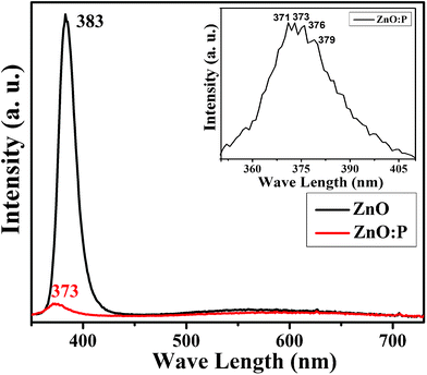 | ||
| Fig. 3 Room-temperature photoluminescence spectra: comparison of pristine ZnO and ZnO:P (5 mol%) nanostructures. The inset shows the magnified UV emission spectral region of ZnO:P nanostructures. | ||
The origin of ferromagnetism in pure ZnO nanostructures has been controversial in the absence of a ferromagnetic metal or metal compound; and structural defects have often been invoked to explain magnetic ordering. Nanoparticles possess a lot of such defect sites because of their comparatively large surface, which, naturally, has many defects in the form of unsaturated bonds. The defects such as Vo, VZn, Vo+, Zni, mechanical stress, and vacancy clusters are considered the main cause for magnetic behaviour in non-magnetic oxides (ZnO, Al2O3, In2O3).42–48 Magnetization curves of pristine and P doped ZnO nanostructures measured at 298 K were shown in Fig. 4. A clear hysteresis loop is observed in the pristine and 5 mol% of P doped ZnO nanostructures with coercivity (Hc) of 30–35 Oe. The magnetization nonlinearly increases with an increase in the applied field. This behaviour is in agreement with the magnetization curve of the ferromagnetic system. The value of magnetisation is 7 × 10⁻⁴ emu g−1 for pristine and 6 × 10⁻⁴ emu g−1 for P doped ZnO nanostructures at a 2000 Oe applied field. There is a slight decrease in the value of magnetization for the ZnO:P samples. Previously, we demonstrated that the magnetism of pristine ZnO nanorods can be switched from ferro- to diamagnetic by annealing in an oxygen-rich atmosphere, resulting in the cancellation of oxygen vacancies (n-type carriers).43 Due to the p-type nature of ZnO:P nanostructures (observed in PL spectra), there is a reduction in the value of magnetization. In our case, single-phased XRD patterns and a slightly shifted ZnO (002) peak with phosphorous doping have been observed. We believe that the detected ferromagnetism in pure and doped nanostructures can be correlated to the oxygen vacancy or zinc interstitial (n-type carriers) related defects exists in the samples. However, the mechanism responsible for the origin of ferromagnetism in pure ZnO nanostructures remains controversial and unclear till now.
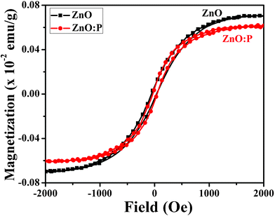 | ||
| Fig. 4 Hysteresis loop (M–H) of pure ZnO and ZnO:P (5 mol%) nanostructures at room temperature. | ||
For unequivocally demonstrating that the incorporated phosphorus atoms actually lead to p-type doping, electrical measurements are required. Recently we reported the mobility enhancement of p-type organic transistors formed using Poly(3-Hexylthi-ophene) (P3HT) using the dispersion of ZnO (zinc oxide) nanostructures.49 In this work, to investigate the effect of phosphorus doping on the electrical properties, current–voltage measurements were performed on both the doped and the undoped nanostructures. For electrical measurements, transistor structures (bottom-gate-top-contact devices) were fabricated as follows. Shadow mask technique was utilized to define source and drain contacts on pure and doped nanostructures. Source and drain metal layers were deposited by RF metal sputtering, consisting of Cr/Au (5 nm/50 nm), where Cr is used as an adhesion layer for Au. The current–voltage characteristics were measured with a probe station under ambient conditions in the dark using a Keithly 2400 semiconductor parameter analyzer. The transistor channel length was 5 μm. Prior to the transistor fabrication, the pure and doped ZnO nanostructures were annealed by a rapid thermal annealing (RTA) system at 600 °C for 10 min to activate the type dopant dominant in the sample. The schematic structure of transistor of pure and doped ZnO nanostructure is shown in Fig. 5a. Fig. 5b presents the gate-dependent drain-source current (Ids) versus voltage (Vds) curves of a representative p-type ZnO:P nanostructures. A quasi linear Idsversus Vds curve under Vg = 0 V indicate that the contact is ohmic. With negatively increasing gate voltage (Vg = 5 V to −5 V), the conductance of the nanostructures increases, revealing a p-type conductivity of the ZnO:P device. To determine the efficiency of the gating behavior and nature of the ZnO:P nanostructure, the transfer characteristics (Ids–Vg) were obtained with a fixed drain-source voltage of −5 V, as shown in Fig. 5c. Fig. 5d presents the room temperature transfer characteristics of a representative n-type ZnO nanorod transistor. The Idsversus Vg curve clearly reveals n-type conductivity of the ZnO nanorods. The electrical studies reveal that p-type characteristics were simultaneously obtained in our synthesized P doped ZnO nanostructures.
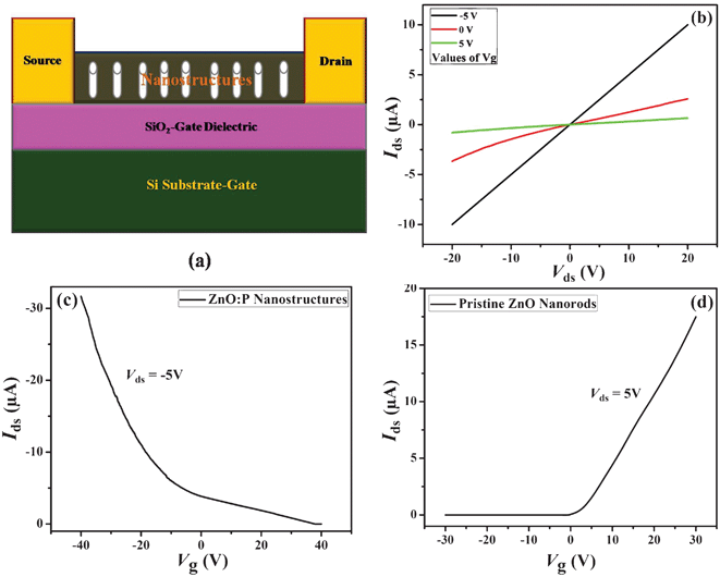 | ||
| Fig. 5 (a) The schematic structure of a back-gated ZnO:P transistor. (b) The Ids–Vds plots of the p-type ZnO:P device at different Vg. (c) Ids–Vg plots of ZnO:P device at Vds = −5 V. (d) Ids–Vg plots of the n-type ZnO transistor device at Vds = 5 V. | ||
Conclusions
In summary, we demonstrate the growth of high-quality well-aligned ZnO:P nanostructures via a simple aqueous based chemical technique. It is found that the structural, optical, electrical, and magnetic properties are sensitively dependent on the incorporation of phosphorous ions in the ZnO lattice sites. The subsequent XRD peak shifts towards the left confirms the effectiveness of the P ion substitutions in the ZnO lattice. The pure and doped nanostructures are single crystals grown along the c-axis [0002] direction, as confirmed by XRD and SAED patterns. But the growth velocity of ZnO:P nanostructures along the [110] direction is distinctly higher than the [001] growth direction, which implies a nanoplatelet structure. The room-temperature PL spectra show that the ZnO nanorods have a strong NBE emission compared to the doped nanostructures. UV emission spectrum of ZnO:P nanoplatelets reveals the acceptor-bound-exciton emission, corroborating the p-type conductivity in nanostructures. In comparison to pristine ZnO nanorods, ZnO:P nanostructures demonstrate a significant enhancement (more than an order of magnitude increase) in ID/IUV value (1–0.056) indicating that more defect centres have been created after doping. The doping of phosphorus ions in ZnO showed a reduction of room temperature ferromagnetism due to the dominance of p-type character in ZnO:P nanoplatelets. A transition from n-type conductivity in undoped ZnO nanorods to a p-type conductivity in ZnO:P nanostructure is achieved by a simple approach.Acknowledgements
The authors thank Prof. D. S. Mishra, Department of Physics, IIT Bombay, for allowing us to use the PLD set up. Financial support from nanomission of Department of Science and Technology (DST), Government of India is greatly acknowledged. The authors are grateful to Centre for Research in Nanotechnology & Science (CRNTS) for TEM facility.References
- Transparent conductive zinc oxide, ed. K. Ellmer, A. Klein and B. Rech, Springer, Berlin, Germany, 2008 Search PubMed.
- S. W. Fana, A. K. Srivastava and V. P. Dravid, Sens. Actuators, B, 2010, 144, 159–163 CrossRef.
- P. Yang, H. Yan, S. Mao, R. Russo, J. Johnson, R. Saykally, N. Morris, J. Pham, R. He and H. J. Choi, Adv. Funct. Mater., 2002, 12, 323–331 CrossRef CAS.
- Ü. Özgür, Y. I. Alivov, C. Liu, A. Teke, M. A. Reshchikov, S. Doğan, V. Avrutin, S.-J. Cho and H. Morkoç, J. Appl. Phys., 2005, 98(041301), 1–104 Search PubMed.
- S. J. Pearton, D. P. Norton, K. Ip, Y. W. Heo and T. Steiner, Prog. Mater. Sci., 2005, 50, 293–340 CrossRef CAS.
- A. A. Lebedev, V. V. Kozlovski, N. B. Strokan, D. V. Davydov, A. M. Ivanov, A. M. Strel'chuk and R. Yakimova, Semiconductors, 2002, 36, 1270–1275 CrossRef CAS.
- F. D. Auret, S. A. Goodman, M. Hayes, M. J. Legodi, H. A. van Laarhoven and D. C. Look, Appl. Phys. Lett., 2001, 79, 3074–3076 CrossRef CAS.
- D. C. Look, D. C. Reynolds, J. W. Hemsky, R. L. Jones and J. R. Sizelove, Appl. Phys. Lett., 1999, 75, 811–813 CrossRef CAS.
- S. B. Zhang, S.-H. Wei and A. Zunger, J. Appl. Phys., 1998, 83, 3192–3196 CrossRef CAS.
- C. H. Park, S. B. Zhang and S.-H. Wei, Phys. Rev. B, 2002, 66(073202), 1–3 Search PubMed.
- M. Joseph, H. Tabata and T. Kawai, Jpn. J. Appl. Phys., 1999, 38, L1205–L1207 CrossRef CAS.
- Y. R. Ryu, S. Zhu, D. C. Look, J. M. Wrobel, H. M. Jeong and H. W. White, J. Cryst. Growth, 2000, 216, 330–334 CrossRef CAS.
- Y. Yan, S. B. Zhang and S. T. Pantelides, Phys. Rev. Lett., 2001, 86, 5723–5726 CrossRef CAS.
- K. Tamura, T. Makino, A. Tsukazaki, M. Sumiya, S. Fuke, T. Furumochi, M. Lippmaa, C. H. Chia, Y. Segawa, H. Koinuma and M. Kawasaki, Solid State Commun., 2003, 127, 265–269 CrossRef CAS.
- Z. Q. Chen, T. Sekiguchi, X. L. Yuan, M. Maekawa and A. Kawasuso, J. Phys.: Condens. Matter, 2003, 15, 1–7 CrossRef.
- B. W. Thomas and D. Walsh, J. Phys. D: Appl. Phys., 1973, 6, 612–615 CAS.
- K. –K. Kim, H. –S. Kim, D. –K. Hwang, J. –H. Lim and S. –J. Park, Appl. Phys. Lett., 2003, 83, 63–65 CrossRef CAS.
- B. Xiang, P. Wang, X. Zhang, S. A. Dayeh, D. P. R. Aplin, C. Soci, D. Yu and D. Wang, Nano Lett., 2007, 7, 323–328 CrossRef CAS.
- K. Minegishi, Y. Koiwai, Y. Kikuchi, K. Yano, M. Kasuga and A. Shimizu, Jpn. J. Appl. Phys., 1997, 36, L1453–L1455 CrossRef CAS.
- X. Zhou, Z. Ye, F. Chen, W. Xu, Y. Miao, J. Huang, J. Lü, L. Zhu and C. B. Zhao, J. Semicond., 2006, 27, 91–95 CAS.
- W. Xu, Z. Ye, T. Zhou, B. Zhao, L. Zhu and J. Huang, Chinese Journal of Semiconductors, 2005, 26, 38–41 CAS.
- J. Yang, H. Kim, J. Lim, D. Hwang, J. Oh and S. Park, J. Electrochem. Soc., 2006, 153, G242–G244 CrossRef CAS.
- P. Wang, N. Chen and Z. Yin, Appl. Phys. Lett., 2006, 88(152102), 1–3 Search PubMed.
- F. X. Xiu, Z. Yang, L. J. Mandalapu and J. L. Liu, Appl. Phys. Lett., 2006, 88(152116), 1–3 Search PubMed.
- D. C. Look, D. C. Reynolds, C. W. Litton, R. L. Jones, D. B. Eason and G. Cantwell, Appl. Phys. Lett., 2002, 81, 1830–1832 CrossRef CAS.
- M. Sun, Q. F. Zhang and J. L. Wu, J. Phys. D: Appl. Phys., 2007, 40, 3798–3802 CrossRef CAS.
- Y. W. Heo, Y. W. Kwon, Y. Li, S. J. Pearton and D. P. Norton, Appl. Phys. Lett., 2004, 84, 3474–3476 CrossRef CAS.
- T. Aoki, Y. Shimizu, A. Miyake, A. Nakamura, Y. Nakanishi and Y. Hatanaka, Phys. Status Solidi B, 2002, 229, 911–914 CrossRef CAS.
- J. Briscoe, D. E. Gallardo and S. Dunn, Chem. Commun., 2009, 10, 1273–1275 RSC.
- Y. J. Hong, H. S. Jung, J. Yoo, Y. J. Kim, C. H. Lee, M. Y. Kim and G. C. Yi, Adv. Mater., 2009, 21, 222–226 CrossRef CAS.
- S. W. Kim, S. Fujita, M. S. Yi and D. H. Yoon, Appl. Phys. Lett., 2006, 88(253114), 1–3 Search PubMed.
- D. S. Kim, J. Fallert, A. Lotnyk, R. Scholz, E. Pippel, S. Senz, H. Kalt, U. Gösele and M. Zacharias, Solid State Commun., 2007, 143, 570–573 CrossRef CAS.
- B. Panigrahy, M. Aslam, D. S. Misra and D. Bahadur, Int. J. Nanosci., 2011, 10, 629–633 CrossRef CAS.
- H. J. Fan, A. S. Barnard and M. Zacharias, Appl. Phys. Lett., 2007, 90(143116), 1–3 Search PubMed.
- R. D. Shannon, Acta Crystallogr., Sect. A: Cryst. Phys., Diffr., Theor. Gen. Crystallogr., 1976, A32, 751–767 CrossRef CAS.
- Y. W. Heo, K. Ip, S. J. Park, S. J. Pearton and D. P. Norton, Appl. Phys. A: Mater. Sci. Process., 2004, 78, 53–57 CrossRef CAS.
- Z. G. Yu, H. Gong and P. Wu, Chem. Mater., 2005, 17, 852–855 CrossRef CAS.
- C. L. Hsu, S. J. Chang, Y. R. Lin, S. Y. Tsaib and I. C. Chen, Chem. Commun. (Cambridge), 2005, 28, 3571–3573 Search PubMed.
- P.-J. Li, Z.-M. Liao, X.-Z. Zhang, X.-J. Zhang, H.-C. Zhu, J.-Y. Gao, K. Laurent, Y. L. Wang, N. Wang and D.-P. Yu, Nano Lett., 2009, 9, 2513–2518 CrossRef CAS.
- C. X. Shan, Z. Liu and S. K. Hark, Appl. Phys. Lett., 2008, 92(073103), 1–3 Search PubMed.
- B. Panigrahy, M. Aslam and D. Bahadur, J. Phys. Chem. C, 2010, 14, 11758–11763 Search PubMed.
- B. Panigrahy, M. Aslam, D. S. Misra, M. Ghosh and D. Bahadur, Adv. Funct. Mater., 2010, 20, 1161–1165 CrossRef CAS.
- A. Sundaresan, R. Bhargavi, N. Rangarajan, U. Siddesh and C. N. R. Rao, Phys. Rev. B, 2006, 74(161306), 1–4 Search PubMed.
- K. Potzger, S. Zhou, J. Grenzer, M. Helm and J. Fassbender, Appl. Phys. Lett., 2008, 92(182504), 1–3 Search PubMed.
- J. B. Yi, H. Pan, J. Y. Lin, J. Ding, Y. P. Feng, S. Thongmee, T. Liu, H. Gong and L. Wang, Adv. Mater., 2008, 20, 1170–1174 CrossRef CAS.
- S. Banerjee, M. Mandal, N. Gayathri and M. Sardar, Appl. Phys. Lett., 2007, 91(182501), 1–3 Search PubMed.
- Q. Xu, H. Schmidt, S. Zhou, K. Potzger, M. Helm, H. Hochmuth, M. Lorenz, A. Setzer, P. Esquinazi, C. Meinecke and M. Grundmann, Appl. Phys. Lett., 2008, 92(082508), 1–3 Search PubMed.
- B. Panigrahy, M. Aslam and D. Bahadur, Appl. Phys. Lett., 2011, 98(183109), 1–3 Search PubMed.
- R. R. Navan, B. Panigrahy, M. S. Baghini, D. Bahadur and V. R. Rao, Composites, Part B, 2012, 43, 1645–1648 CrossRef CAS.
Footnote |
| † Electronic supplementary information (ESI) available. See DOI: 10.1039/c2ra20441j |
| This journal is © The Royal Society of Chemistry 2012 |