Electronic and magnetic properties of boron nitride nanoribbons with topological line defects
Peizhe
Tang
a,
Xiaolong
Zou
a,
Shanying
Wang
a,
Jian
Wu
a,
Haitao
Liu
b and
Wenhui
Duan
*a
aDepartment of Physics and State Key Laboratory of Low-Dimensional Quantum Physics, Tsinghua University, Beijing 100084, People's Republic of China. E-mail: dwh@phys.tsinghua.edu.cn
bThe Key Laboratory of Computational Physics, Institute of Applied Physics and Computational Mathematics, P. O. Box 8009, Beijing 100088, People's Republic of China
First published on 25th April 2012
Abstract
Spin-polarized first-principles calculations show that in contrast to pristine boron nitride nanoribbons (BNNRs), the hybrid BNNRs with topological line defects exhibit diverse electronic and magnetic properties. It is interesting to find that with no need for selective edge functionalization, hybrid BNNRs can exhibit half-metallicity and half-semi-metallicity, dependent on the type of edge and line defect. Furthermore, an applied tensile strain can tune the half-semi-metal gap and stabilize the ferromagnetic ordering of the ground state. For hybrid BNNRs with two zigzag edges saturated, the tailoring of line defect state makes the band gap smaller. This work provides a possibility of making spintronic devices based on hybrid BNNRs with line defects and an interesting way of fabricating metal-free half-metal.
Introduction
Quasi one-dimensional (1D) sp materials such as graphene nanoribbons (GNRs),1,2 boron nitride nanoribbons (BNNRs)3–6 and C–BN nanoribbons,7,8 have attracted much attention recently due to their intriguing physical properties and potential nanoelectronic applications. In addition, first-principles calculations have predicted that half-metallicity (i.e., one of the spin channels showing insulating behavior and the other being metallic) can be achieved in zigzag GNRs and BNNRs via applying external transverse electric fields,1,4,6,9 or selective chemical functionalizations.4,9–12 However, the required rigorous conditions of high electric field and selective functionalization are difficult to achieve in current experiments. For practical spintronic applications, it is interesting and crucial to find some new quasi 1D sp materials with intrinsic half-metallicity.The grain boundaries (GBs) in two dimensional structures, which can be described as extended topological line defects,13 are almost unavoidable in large area synthesis of graphene14,15 and layered hexagonal boron nitride (h-BN).16,17 The topographies of GBs in graphene have been identified experimentally14,15,18,19 and theoretically13,20,21 as a line defect which may be composed of octagonal and pentagonal carbon rings. Although the detailed structure of the GBs observed in h-BN on Ni(111) by scanning tunneling microscopy16 are not clearly identified yet, the formation mechanism of this line defect is similar to that of GBs in graphene. On the other hand, several methods such as etching22,23 and electron beam irradiation24 could be used to cut the layered material into nanoribbons, which makes it possible to fabricate GNRs and BNNRs with GBs. GBs in graphene can change the lattice orientations,20 tune the features of the ribbon edges, and more importantly, induce half-metallicity.21 For BNNRs, half-metallicity can be achieved when the N edge is bare and the B edge is selectively saturated,11 which originates from localized lone-pair edge states and dangling-bond states in the bare N edge. Since the existence of GBs will change the crystalline orientation, hybrid BNNRs with GBs can have two bare N edges (i.e., no B edges), suggesting the possibility that the half-metallicity could be realized without introducing selective chemical adsorption or high external electric fields.
In this work, using first-principles calculations, we study structural, electronic and magnetic properties of hybrid BNNRs. Two types of hybrid BNNRs are considered. One is composed of two zigzag nanoribbons (denoted ZZ-BNNRs) joined by a line defect of octagonal and pentagonal rings. The other is composed of a zigzag nanoribbon and an armchair nanoribbon (denoted ZA-BNNRs) joined by a line defect of heptagonal and pentagonal rings. It is found that ZZ-BNNRs with two bare N edges can exhibit half-metallicity with both N edges being the spin polarized transport channels. When the two edges of hybrid ZZ-BNNRs are saturated by H atoms, the B-B pairs in the line defect could reduce the gap effectively. In contrast, ZA-BNNRs with only one bare N edge exhibit half-semi-metallicity (i.e., one of the electron spins shows insulating behavior and the other shows narrow-gap semiconducting behavior25). Moreover, the half-semi-metal gap can be tuned by an applied strain, leading to stabilization of the ferromagnetic ordering. Under the uniaxial strain of 7.5%, the carriers of ZA-BNNRs are 100% spin polarized, and the half-semi-metal gap increases to 228 meV, large enough for operating the single-spin state at room temperature. Our results demonstrate the potential of hybrid BNNRs in the spintronic applications.
Models and method
The structures of hybrid BNNRs are shown in Fig. 1. The line defect in ZZ-BNNRs (Fig. 1(a) to 1(d)) is composed of an array of pairs of pentagons and octagons (called as the 5-5-8 chain hereafter), and that in ZA-BNNRs (Fig. 1(e) and 1(f)) contains a linear array of pentagons and heptagons (called as the 5-7 chain hereafter). The two zigzag edges of ZZ-BNNRs are chosen as the same type (i.e., two N edges or two B edges). ZZ-BNNRs with H-passivated N (B) edges or bare N (B) edges are denoted respectively, ZZ-BNNR-NH (ZZ-BNNR-BH) and ZZ-BNNR-N (ZZ-BNNR-B). In contrast, ZA-BNNRs have only one zigzag edge. ZA-BNNRs with one bare zigzag N (B) edge is denoted ZA-BNNR-N (ZA-BNNR-B). These hybrid BNNRs are further labeled by the number of zigzag BN chains along the x direction, which defines the width of the ribbons. The hybrid BNNRs with n B-N chains in the left part and m B–N chains in the right part are denoted ZZ-(n,m)-BNNR or ZA-(n,m)-BNNR. It should be noted that hybrid ZZ-BNNRs with one B edge and one N edge are not considered here: more B–B and N–N bonds are formed in the topological line defects of these structures, which results in much higher formation energies. In this work, ZZ-(7,7)-BNNR and ZA-(7,6)-BNNR are chosen as representative models of hybrid BNNRs.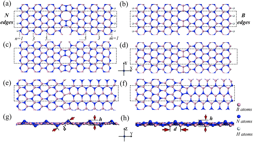 | ||
| Fig. 1 Geometrical structures of boron nitride nanoribbons with 1-D line defects: (a) ZZ-(7,7)-BNNR-NH; (b) ZZ-(7,7)-BNNR-BH; (c) ZZ-(7,7)-BNNR-N; (d) ZZ-(7,7)-BNNR-B; (e,g) ZA-(7,6)-BNNR-N (top view, side view); (f, h) ZA-(7,6)-BNNR-B (top view, side view). The ribbons are infinitely long along the y direction. The dashed rectangles denote the unit cell of the systems. d′ and d are the distances between neighboring N edge atoms in ZA-(7,6)-BNNR-N and the distance between neighboring B edge atoms in ZA-(7,6)-BNNR-B. And h is the average shift of the bridge N atoms from the basal plane. | ||
The spin polarized density functional theory calculations are performed using the Vienna ab initio simulation package (VASP),26 with the exchange–correlation potential described by local spin density approximation (LSDA) functional.27 The projector augmented wave (PAW) potentials28 are employed with a cut off energy of 450 eV for the plane wave expansion. The full structural optimizations are carried out by 1 × 10 × 1 Monkhorst–Pack k points sampling until the residual forces on atoms are less than 0.01 eV Å−1. In the self-consistent total-energy calculations, the Brillouin zone (BZ) is sampled by 1 × 30 × 1 Monkhorst–Pack k points. A vacuum layer of 12 Å is used to avoid the spurious interaction between two adjacent ribbons. The strain is applied along the topological defect line (the y direction).
Results and discussion
A. Geometrical structures
An essential structural feature of the hybrid BNNRs is the formation of the N–N or B–B bonds in the line defect. The N–N bond length in the 5-5-8 chain of ZZ-(7,7)-BNNR-NH and ZZ-(7,7)-BNNR-N is about 1.46 Å. The three associated bond angles are approximately 108.5°, 108.5° and 143°, significantly deviating from the standard sp2 bond angle (120°). The B-B bond length in the 5-5-8 chain of ZZ-(7,7)-BNNR-BH and ZZ-(7,7)-BNNR-B is about 1.65 Å, and the three associated bond angles are approximately 107.5°, 107.5°, and 145°, close to the bond angles around the N–N bond. It is found that the planar structure is maintained in all hybrid ZZ-BNNRs.For ZA-(7,6)-BNNR-N and ZA-(7,6)-BNNR-B, besides the formation of B–B bonds (1.66 Å) or N–N bonds (1.40 Å) in the 5-7 chain, the hexagonal network is significantly distorted due to the incommensurability of the zigzag and armchair segments (see Fig. 1(e) –1(h)). The average B–N bond lengths along the x direction in zigzag and armchair segments of the hybrid system are similar to that of pristine BNNRs. In contrast, the average B–N bond length along the y direction in the zigzag segment is 1.38 Å, shorter than that of pristine BNNRs (1.45 Å). And the bond length in the armchair part is 1.53 Å, larger than that of pristine BNNRs. In comparison with the pristine BNNRs, the armchair segment is under tension whereas the zigzag segment is under compression along the y direction, which is induced by the incommensurability of the hybrid structure. It is found that an in-plane reconstruction occurs at the armchair edges, similar to pristine armchair BNNRs without H passivation.29 In particular, an out-of-plane reconstruction of the zigzag edge can be observed due to the compression in the zigzag segment. The distance between two adjacent B edge atoms in ZA-(7,6)-BNNR-B (d in Fig. 1(h)) decreases from 2.33 to 1.89 Å, and the associated bridge N atoms move out from the basal plane after reconstruction. In contrast, the bridged N atoms in ZA-(7,6)-BNNR-N (Fig. 1(g)) stay at opposite sides of the basal plane, thus the distance between them (d′ in Fig. 1(g)) becomes larger owing to the out-of-plane reconstruction. The out-of-plane reconstruction can be quantitatively described by the average shift of the bridge N atoms from the basal plane (h in Fig. 1(g) and 1(h)). The h of ZA-(7,6)-BNNR-N is 0.05 Å, larger than that of ZA-(7,6)-BNNR-B (0.03 Å). All these structural deformations and edge reconstructions will dramatically affect electronic and magnetic properties of the hybrid BNNRs.
B. Electronic and magnetic properties
For ZZ-(7,7)-BNNR-N, our calculations show that the spin configuration (++, ++) and (++, −−) are degenerate ground states with magnetic moment of 1 μB per edge N atom. In this case, the coupling between the two ferromagnetic N edges is relatively weak, partially due to the existence of the GB in the structure. More importantly, the energy of spin configuration (++, ++) is 60 meV/(edge atom) and 82 meV/(edge atom) lower than those of spin configuration (+−, +−) and nonmagnetic phase respectively. Since no edge reconstruction occurs, this ferromagnetism results from the exchange interaction between the dangling-bond electrons in pristine zigzag BNNRs with passivated B edge,11 which was also observed in partially hydrogenated Si (111) surfaces.30Fig. 2(a) and 2(c) display the band structures of ZZ-(7,7)-BNNR-N in spin configurations (++, ++) and (++, −−), respectively. It can be seen that the (++, ++) configuration is half-metallic, but the (++, −−) one is metallic with spin-degenerate bands.
![Band structures of (a) ZZ-(7,7)-BNNR-N with spin configuration (++, ++), (c) ZZ-(7,7)-BNNR-N with spin configuration (++, −−) and (d) ZZ-(5,5)-BNNR-N with spin configuration (++, ++). The Fermi level (dashed line) is set to zero. Red and black lines stand for spin-majority and spin-minority states, respectively. (b) Partial charge density of the γ, α and β bands at different k points. The spatial distribution of the charge difference between spin-majority and spin-minority [ρ↑(r) − ρ↓(r)] for (e) ZZ-(7,7)-BNNR-N with spin configuration (++, ++) and (f) ZZ-(7,7)-BNNR-N with spin configuration (++, −−). Green/red is for spin majority/minority. The isovalue is 0.01 e Å−3.](/image/article/2012/RA/c2ra20306e/c2ra20306e-f2.gif) | ||
| Fig. 2 Band structures of (a) ZZ-(7,7)-BNNR-N with spin configuration (++, ++), (c) ZZ-(7,7)-BNNR-N with spin configuration (++, −−) and (d) ZZ-(5,5)-BNNR-N with spin configuration (++, ++). The Fermi level (dashed line) is set to zero. Red and black lines stand for spin-majority and spin-minority states, respectively. (b) Partial charge density of the γ, α and β bands at different k points. The spatial distribution of the charge difference between spin-majority and spin-minority [ρ↑(r) − ρ↓(r)] for (e) ZZ-(7,7)-BNNR-N with spin configuration (++, ++) and (f) ZZ-(7,7)-BNNR-N with spin configuration (++, −−). Green/red is for spin majority/minority. The isovalue is 0.01 e Å−3. | ||
For half-metallic ZZ-(7,7)-BNNR-N, the spin-majority channel (left panel of Fig. 2(a)) shows a band gap of 3.33 eV, while the spin-minority channel is metallic (right panel of Fig. 2(a)). In such a system, the carrier transport is totally dominated by spin-minority electrons and the current flow would be completely spin polarized. The half-metal gap, defined as the energy difference between the Fermi level and the valence band maximum (VBM) of spin-majority channel, is 34.5 meV. Different from the pristine zigzag BNNRs with passivated B edge,11 the hybrid ZZ-BNNR-N has two spin polarized transport channels at both N edges due to its unique geometrical structure.
Interestingly, half-metallicity in ZZ-(7,7)-BNNR-N may be stabilized by applying an external magnetic field and hybrid ZZ-BNNR-N shows massless Dirac-fermion behaviors: a linear band crossing at the Fermi level can be clearly observed. The partial charge density distributions of γ (at X point), α (at X point), β (at Γ, M, and X points) and δ (at M point) bands are plotted in Fig. 2(b) Similar to the results of pristine zigzag BNNRs with passivated B edge,11 the two-fold degenerate α band originates from dangling-bond states of N edges, while the δ band is contributed by lone-pair states. The wavefunctions of α and δ bands are, respectively, symmetric and antisymmetric with respect to the basal plane. So no gap is created at the crossing of α and δ bands. The β band exhibits very different characteristics from the α and δ bands. As shown in Fig. 2(b), at X point β state is well localized at the 5-5-8 line defect (line defect state), while at Γ point it is mainly composed of the pz orbitals of edge N atoms (lone-pair state) and degenerate with the δ band. At the k point between them (such as M point), the partial charge density distributes at line defect and both edges due to the hybridization of the line defect state and the lone-pair states (Fig. 2(b)-βM). The hybridization opens a gap below the Fermi level (ΔEG in Fig. 2(a) and 2(d)), which is strongly dependent on the ribbon width. Fig. 2(d) shows the half-metallic band structure of narrower hybrid ZZ-(5,5)-BNNR-N, which is very similar to that of ZZ-(7,7)-BNNR-N. However, ΔEG in ZZ-(5,5)-BNNR-N is 156 meV, much larger than that in ZZ-(7,7)-BNNR-N (70 meV). The half-metallicity is also enhanced with the half-metal gap increased by 11.5 meV. This suggests that the coupling between the edge state and line defect state can be used to enhance the half-metallicity by changing the ribbon width.
Although the states localized at the 5-8-5 line defect play a key role in the half-metallicity in this hybrid system, the spin-polarization results from only the N edges, as can be easily seen from the spatial distributions of the charge difference between spin-majority and spin-minority in Fig. 2(e) and 2(f). Moreover, our results on asymmetric ZZ-(7,3)-BNNR-N show similar band structures, with the magnetic moments of the edge atoms hardly changed. The half-metallic gap increases to 85.7 meV. These render the robust half-metallicity and magnetism in this system, which is in sharp contrast to the case of the GNRs embedded with Stone-Wales defects.31
For ZZ-(7,7)-BNNR-B, the (+−, +−) configuration is the most stable state, about 20 meV/(edge atom) lower in energy than the (++, −−) configuration. Both spin configurations exhibit semiconducting behavior with spin-degenerate bands, as shown in Fig. 3(a). The magnetic properties are determined by the two bare B edges as seen from the spatial distribution of the charge difference between spin-majority and spin-minority in Fig. 3(c). The average magnetic moment on the edge B atom is 0.76 μB. These results are very similar to those of pristine BNNRs with H-passivated N edge and bare B edge.11 The band gap of ZZ-(7,7)-BNNR-B with (+−, +−) configuration is 1.00 eV, which is even smaller than that of pristine ZBNNR-NH (1.89 eV).11 As shown in Fig. 3(d), the bottom of the conduction bands in ZZ-(7,7)-BNNR-B with (+−,+−) configuration is localized at the line defect, while the top of the valence band is contributed by the edge states. Due to the existence of both the line defect and bared B edges, the band gap is reduced remarkably.
![Band structures of (a) ZZ-(7,7)-BNNR-B and (b) ZZ-(7,7)-BNNR-BH, ZZ-(7,7)-BNNR-NH. The Fermi level (dashed line) is set to zero. (c) The spatial distribution of the charge difference between spin-majority and spin-minority [ρ↑(r) − ρ↓(r)] for ZZ-(7,7)-BNNR-B with spin configuration (+−, +−). Green is for spin majority and red is for spin minority. (d) Partial charge density of the α′, β′ bands at Γ point. (e) Partial charge density of the α and γ bands at the X point, and β and δ bands at the Γ point. The isovalue is 0.01 e Å−3.](/image/article/2012/RA/c2ra20306e/c2ra20306e-f3.gif) | ||
| Fig. 3 Band structures of (a) ZZ-(7,7)-BNNR-B and (b) ZZ-(7,7)-BNNR-BH, ZZ-(7,7)-BNNR-NH. The Fermi level (dashed line) is set to zero. (c) The spatial distribution of the charge difference between spin-majority and spin-minority [ρ↑(r) − ρ↓(r)] for ZZ-(7,7)-BNNR-B with spin configuration (+−, +−). Green is for spin majority and red is for spin minority. (d) Partial charge density of the α′, β′ bands at Γ point. (e) Partial charge density of the α and γ bands at the X point, and β and δ bands at the Γ point. The isovalue is 0.01 e Å−3. | ||
Following on, we turn to the effects of the edge passivation. As shown in Fig. 3(b), the electronic structures of ZZ-(7,7)-BNNR-BH and ZZ-(7,7)-BNNR-NH exhibit typical non-magnetic semiconducting behaviors, similar to those of the pristine BNNRs passivated by H atoms.6,11 However, the band gaps of these hybrid ribbons are reduced tremendously due to the introduction of the 5-5-8 chain. In detail, the band gaps of ZZ-(7,7)-BNNR-BH and ZZ-(7,7)-BNNR-NH are 2.50 and 3.30 eV respectively, which are much smaller than those of h-BN (4.53 eV)5 and 8-ZBNNR-H (3.90 eV)11 by the LSDA calculations. Fig. 3(e) shows the partial charge density of the VBM (i.e., α band and γ band at X point) and conduction band minimum (CBM) (i.e., β band and δ band at Γ point). It can be seen that for ZZ-(7,7)-BNNR-BH, both the α and β bands are mainly contributed by the line defect. This indicates that the energy difference between the bonding and antibonding states of B-B bonds determines the band gap. For ZZ-(7,7)-BNNR-NH, the γ band is mainly contributed by the center N–N pairs of the line defect and δ band is well localized at the B atoms of the line defect. The line defect with B–B pairs can reduce the band gap more strongly than that with N–N pairs. Therefore, introducing topological line defects, especially the 5-5-8 chain with B–B bonds, is probably an efficient way to substantially reduce the band gap of BN systems. These interesting electronic properties will make hybrid ZZ-BNNRs with H-passivation promising for potential applications, particularly in nanoelectronics.
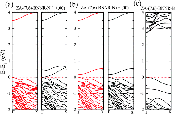 | ||
| Fig. 4 (a, b) Band structures of ZA-(7,6)-BNNR-N in the (++, 00) and (+−, 00) spin configurations. The Fermi level (dashed line) is set to zero. Red and black lines stand for spin-majority and spin-minority states, respectively. (c) Band structure of ZA-(7,6)-BNNR-B, which is nonmagnetic. | ||
![The half-semi-metal gap of ZA-(7,6)-BNNR-N as a function of the tensile strain η along the y direction. The band structures around the Fermi level are shown for ZA-(7,6)-BNNR-N under different strain as the inserts: (a) η = 0, (b) η = 2.15% and (c) η = 7.53%. The Fermi level (dashed line) is set to zero. Red and black lines stand for spin-majority and spin-minority states, respectively. Partial charge densities of the α, β, γ and δ bands at Γ point are also shown in the insets. The spatial distribution of the charge difference between spin-majority and spin-minority [ρ↑(r) − ρ↓(r)] for ZA-(7,6)-BNNR-N with (d) η = 0 and (e) η = 7.53%. Green/red is for spin majority/minority. The isovalue is 0.01 e Å−3.](/image/article/2012/RA/c2ra20306e/c2ra20306e-f5.gif) | ||
| Fig. 5 The half-semi-metal gap of ZA-(7,6)-BNNR-N as a function of the tensile strain η along the y direction. The band structures around the Fermi level are shown for ZA-(7,6)-BNNR-N under different strain as the inserts: (a) η = 0, (b) η = 2.15% and (c) η = 7.53%. The Fermi level (dashed line) is set to zero. Red and black lines stand for spin-majority and spin-minority states, respectively. Partial charge densities of the α, β, γ and δ bands at Γ point are also shown in the insets. The spatial distribution of the charge difference between spin-majority and spin-minority [ρ↑(r) − ρ↓(r)] for ZA-(7,6)-BNNR-N with (d) η = 0 and (e) η = 7.53%. Green/red is for spin majority/minority. The isovalue is 0.01 e Å−3. | ||
It is well known that applying external strain can effectively tune electronic and magnetic properties of graphene and related materials.33,34 For example, the energy gap, subband spacing, and spatial distributions of electronic wave functions of the armchair graphene nanoribbons can be modified by the strain.33 In consideration of the intrinsic stress induced by the incommensurability of the zigzag and armchair segments in the hybrid ZA-BNNRs, we further explore the effect of an applied uniaxial tensile strain on their half-semi-metallicity. It can be expected that the tensile strain would enhance the B-N bond length of the zigzag segment along the y direction, recover the original magnetic properties of bare zigzag N-edges, and consequently tune the ferromagnetism of the system. Herein, the applied tensile strain is defined as η = (r − r0)/r0, where r and r0 are the deformed and equilibrium lattice constants along the axial direction (y direction in Fig. 1).
As demonstrated in Fig. 5, the half-semi-metal gap monotonously increases with increasing tensile strain. Typically, the half-semi-metal gap of ZA-(7,6)-BNNR-N is 21 meV under zero strain, but increases to 228 meV under a tensile strain of 7.53%. This value is about 8 times larger than kB T at T = 300 K, and is comparable to the half-metal gap of ZGNRs under high electric field1 and large enough for room-temperature operation. Moreover, the energy difference between the (++, 00) and (+−, 00) spin configurations increases from 2.5 meV/(edge atom) to 30 meV/(edge atom). Clearly, the tensile strain applied to ZA-(7,6)-BNNR-N could tune the half-semi-metal gap and stabilize the ferromagnetic ordering of the ground state.
The evolution of the band structures and partial charge densities with strain are also shown for ZA-(7,6)-BNNR-N in the insets of Fig. 5. It can be seen that the VBM in the spin-majority channel (β band and γ band at Γ point) is mainly contributed by the armchair edge (Fig. 5-βΓ and 5-γΓ). Due to the out-of-plane reconstruction of the N-edge, the VBM and CBM in the spin-minority channel (Fig. 5-αΓ) show different features from those in ZZ-BNNR-N. The sp2 bonding between the edge N atom and the neighboring B atoms is strongly distorted, and the distance between the neighboring edge N atoms increases. As a result, the direct exchange interaction between dangling bonds decreases, which weakens the ferromagnetic ordering of the system. When a tensile strain is applied, the out-of-plane distortion of the N edge in the zigzag segment (originally compressed in ZA-BNNRs) is greatly reduced. This leads to the recovery of the sp2 hybridization at the zigzag N-edge and the stabilization of the ferromagnetic ordering. Correspondingly, the characteristics of the band structure around the Fermi level, dominated by the zigzag N-edge states (Fig. 5-δΓ), become similar to those of pristine zigzag BNNRs11 and hybrid ZZ-BNNRs except for a gap-opening at the Dirac point. The gap-opening originates from the symmetry breaking in ZA-BNNRs: the coupling between the dangling-bond state and lone-pair state occurs since the dangling-bond state is not completely anti-symmetric with respect to the basal plane, due to the incommensurability of the zigzag and armchair segments.
Conclusions
In summary, structural, electronic and magnetic properties of hybrid BNNRs with topological line defects are investigated using first-principles calculations. Two types of line defect are considered. One is the 5-5-8 chain joining two zigzag segments, and the other is the 5-7 chain joining a zigzag segment with an armchair segment. It is found that hybrid zigzag-zigzag BNNRs with two bare N edges can exhibit half-metallicity. In this case, both N edges can act as the spin-polarized transport channels, and the half-metallic gap increases with decreasing ribbon width. Differently, hybrid zigzag-zigzag BNNRs with two bare B edges are antiferromagnetic and semiconducting with a significantly reduced band gap. For hybrid zigzag-armchair BNNRs, a sizable out-of-plane distortion occurs at the zigzag edge. A half-semi-metallic behavior is observed in the zigzag-armchair BNNRs with one bare N edge. The half-semi-metal gap and ferromagnetic stability can be manipulated by applying an uniaxial strain. More importantly, to achieve half-metallicity and half-semi-metallicity, rigorous selective chemical decorations or a high external electric field is not required in these hybrid systems. These properties make the hybrid BNNRs with line defects attractive candidates for future nanoscale spintronics devices, such as spin filter, nanomemory elements, and nanotransistors.Acknowledgements
This work was supported by the Ministry of Science and Technology of China (Grant Nos. 2011CB606405 and 2011CB921901), the National Natural Science Foundation of China (Grant No. 11074139).References
- Y. W. Son, M. L. Cohen and S. G. Louie, Nature, 2006, 444, 347 CrossRef CAS.
- (a) Y. W. Son, M. L. Cohen and S. G. Louie, Phys. Rev. Lett., 2006, 97, 216803 CrossRef; (b) Q. M. Yan, B. Huang, J. Yu, F. W. Zheng, J. Zang, J. Wu, B. L. Gu, F. Liu and W. H. Duan, Nano Lett., 2007, 7, 1469 CrossRef CAS; (c) Z. Y. Li, H. Y. Qian, J. Wu, B. L. Gu and W. H. Duan, Phys. Rev. Lett., 2008, 100, 206802 CrossRef; (d) W. Chen, Y. Li, G. Yu, Z. Zhou and Z. F. Chen, J. Chem. Theory Comput., 2009, 5, 3088 CrossRef CAS; (e) J. Li, Z. Y. Li, G. Zhou, Z. Liu, J. Wu, B. -L. Gu, J. Ihm and W. H. Duan, Phys. Rev. B: Condens. Matter Mater. Phys., 2010, 82, 115410 CrossRef; (f) Q. Tang, Z. Zhou and Z. F. Chen, J. Phys. Chem. C, 2011, 115, 18531 CAS.
- D. Golberg, D. Bando, Y. Huang, T. Terao, M. Mitome, C. Tang and C. Zhi, ACS Nano, 2010, 4, 2979 CrossRef CAS.
- O. Hod, V. Barone, J. E. Peralta and G. E. Scuseria, Nano Lett., 2007, 7, 2295 CrossRef CAS.
- (a) C. H. Park and S. G. Louie, Nano Lett., 2008, 8, 2200 CrossRef CAS; (b) Z. Zhang and W. Guo, Phys. Rev. B: Condens. Matter Mater. Phys., 2008, 77, 075403 CrossRef; (c) F. Zheng, Z. Liu, J. Wu, W. H. Duan and B.-L. Gu, Phys. Rev. B: Condens. Matter Mater. Phys., 2008, 78, 085423 CrossRef; (d) H. Zeng, C. Zhi, Z. Zhang, X. Wei, X. Wang, W. Guo, Y. Bando and D. Golberg, Nano Lett., 2010, 10, 5049 CrossRef CAS.
- V. Barone and J. E. Peralta, Nano Lett., 2008, 8, 2210 CrossRef CAS.
- (a) A. Du, Y. Chen, Z. Zhu, G. Lu and S. C. Smith, J. Am. Chem. Soc., 2009, 131, 1682 CrossRef CAS; (b) E. Kan, X. Wu, Z. Li, X. C. Zeng, J. L. Yang and J. G. Hou, J. Chem. Phys., 2008, 129, 084712 CrossRef.
- B. Huang, H. K. Lee, B.-L. Gu, F. Liu and W. H. Duan, Nano Res., 2012, 5, 62 CrossRef CAS.
- Z. Y. Li, B. Huang and W. H. Duan, J. Nanosci. Nanotechnol., 2010, 10, 5374 CrossRef CAS.
- Y. G. Zhou, P. Yang, G. Wang, X. T. Zu, H. Y. Xiao, X. Sun, M. A. Khaleel and F. Gao, Phys. Chem. Chem. Phys., 2011, 13, 7378 RSC.
- F. Zheng, G. Zhou, Z. Liu, J. Wu, W. H. Duan, B.-L. Gu and S. B. Zhang, Phys. Rev. B: Condens. Matter Mater. Phys., 2008, 78, 205415 CrossRef.
- (a) E. J. Kan, Z. Y. Li, J. L. Yang and J. G. Hou, J. Am. Chem. Soc., 2008, 130, 4224 CrossRef CAS; (b) Y. Li, Z. Zhou, P. Shen and Z. Chen, ACS Nano, 2009, 3, 1952 CrossRef CAS; (c) W. Chen, Y. Li, G. Yu, C. Li, S. B. Zhang, Z. Zhou and Z. Chen, J. Am. Chem. Soc., 2010, 132, 1699 CrossRef CAS; (d) M. Wu, X. Wu and X. C. Zeng, J. Phys. Chem. C, 2010, 114, 3937 CrossRef CAS; (e) Y. Wang, Y. Ding and J. Ni, Phys. Rev. B: Condens. Matter Mater. Phys., 2010, 81, 193407 CrossRef; (f) X. H. Zheng, X. L. Wang, T. A. Abtew and Z. Zeng, J. Phys. Chem. C, 2010, 114, 4190 CrossRef CAS; (g) A. Lopez-Bezanilla, J. Huang, H. Terrones and B. G. Sumpter, Nano Lett., 2011, 11, 3267 CrossRef CAS; (h) M. Wu, X. Wu, Y. Pei and X. Zeng, Nano Res., 2011, 4, 233 CrossRef CAS.
- O. V. Yazyev and S. G. Louie, Phys. Rev. B: Condens. Matter Mater. Phys., 2010, 81, 195420 CrossRef.
- P. Y. Huang, C. S. Ruiz-Vargas, A. M. Van der Zande, W. S. Whitney, M. P. Levendorf, J. W. Kevek, S. Garg, J. S. Alden, C. J. Hustedt, Y. Zhu, J. Park, P. L. McEuen and D. A. Muller, Nature, 2011, 469, 389 CrossRef CAS.
- K. Kim, Z. Lee, W. Regan, C. Kisielowski, M. F. Crommie and A. Zettl, ACS Nano, 2011, 5, 2142 CrossRef CAS.
- W. Auwärter, M. Muntwiler, J. Osterwalder and T. Greber, Surf. Sci., 2003, 545, L735 CrossRef.
- W. Auwärter, M. Muntwiler, T. Greber and J. Osterwalder, Surf. Sci., 2002, 511, 379 CrossRef.
- J. Lahiri, Y. Lin, P. Bozkurt, I. I. Oleynik and M. Batzill, Nat. Nanotechnol., 2010, 5, 326 CrossRef CAS.
- J. An, E. Voelkl, J. S. Suk, X. Li, C. W. Magnuson, L. Fu, P. Tiemeijer, M. Bischoff, B. Freitag, E. Popova and R. S. Ruoff, ACS Nano, 2011, 5, 2433 CrossRef CAS.
- O. V. Yazyev and S. G. Louie, Nat. Mater., 2010, 9, 806 CrossRef CAS.
- A. R. Botello-Méndez, E. Cruz-Silva, F. López-Urías, B. G. Sumpter, V. Meunier and M. Terrones, ACS Nano, 2009, 3, 3606 CrossRef.
- X. R. Wang and H. J. Dai, Nat. Chem., 2010, 2, 661 CrossRef CAS.
- P. Sutter, J. Lahiri, P. Albrecht and E. Sutter, ACS Nano, 2011, 5, 7303 CrossRef CAS.
- J. H. Warner, M. H. Rümmeli, A. Bachmatiuk and B. Büchner, ACS Nano, 2010, 4, 1299 CrossRef CAS.
- J. M. Pruneda, Phys. Rev. B: Condens. Matter Mater. Phys., 2010, 81, 161409 CrossRef.
- G. Kresse and J. Hafner, Phys. Rev. B: Condens. Matter, 1994, 49, 14251 CrossRef CAS.
- D. M. Cererley and B. J. Alder, Phys. Rev. Lett., 1980, 45, 566 CrossRef.
- G. Kresse and D. Joubert, Phys. Rev. B: Condens. Matter Mater. Phys., 1999, 59, 1758 CrossRef CAS.
- R. Mukherjee and S. Bhowmick, J. Chem. Theory Comput., 2011, 7, 720 CrossRef CAS.
- (a) S. Okada, K. Shiraishi and A. Oshiyama, Phys. Rev. Lett., 2003, 90, 026803 CrossRef; (b) Z. Zhang, W. Guo and X. C. Zeng, Phys. Rev. B: Condens. Matter Mater. Phys., 2010, 82, 235423 CrossRef.
- P. Lu, Z. Zhang and W. Guo, Phys. Lett. A, 2009, 373, 3354 CrossRef CAS.
- S. G. Hao, G. Zhou, W. H. Duan, J. Wu and B. L. Gu, J. Am. Chem. Soc., 2006, 128, 8453 CrossRef CAS.
- (a) L. Sun, Q. Li, H. Ren, H. B. Su, Q. W. Shi and J. L. Yang, J. Chem. Phys., 2008, 129, 074704 CrossRef; (b) Y. Li, X. W. Jiang, Z. F. Liu and Z. R. Liu, Nano Res., 2010, 3, 545 CrossRef CAS.
- (a) F. Guinea, M. I. Katsnelson and A. K. Geim, Nat. Phys., 2009, 6, 30 CrossRef; (b) S. M. Choi, S. H. Jhi and Y. W. Son, Nano Lett., 2010, 10, 3486 CrossRef CAS; (c) N. Levy, S. A. Burke, K. L. Meaker, M. Panlasigui, A. Zettl, F. Guinea, A. H. Castro Neto and M. F. Crommie, Science, 2010, 329, 544 CrossRef CAS; (d) L. Kou, C. Tang, W. Guo and C. Chen, ACS Nano, 2011, 5, 1012 CrossRef CAS.
| This journal is © The Royal Society of Chemistry 2012 |