Surface charge transfer doping of germanium nanowires by MoO3 deposition
Lin-Bao
Luo
*a,
Tsz-Wai
Ng
b,
Hao
Tang
b,
Feng-Xia
Liang
b,
Yu-Cheng
Dong
b,
Jian-Sheng
Jie
*a,
Chun-Yan
Wu
a,
Li
Wang
a,
Zhi-Feng
Zhu
a,
Yong-Qiang
Yu
a and
Qiang
Li
a
aSchool of Electronic Science and Applied Physics, Hefei University of Technology, Hefei, Anhui 230009, P. R. China. E-mail: luolb@hfut.edu.cn (L. B. Luo); jsjie@hfut.edu.cn (J. S. Jie)
bDepartment of Physics and Materials Science, City University of Hong Kong, Kowloon, Hong Kong SAR, P. R. China
First published on 2nd February 2012
Abstract
We report on the surface transfer p-type doping of germanium nanowires (GeNWs) via MoO3 thin film deposition. The GeNWs studied were prepared by a conventional thermal evaporation approach. Electrical property analysis shows that the conductance, hole mobility and concentration were all prominently enhanced after MoO3 thin film coating. Such a remarkable surface doping effect can be attributed to the surface charge transfer at the GeNWs/MoO3 interface, which is verified by in situ XPS analysis of GeNWs as a function of increasing MoO3 coverage. Further hole mobility and concentration evolution study of MoO3/GeNWs reveals that the GeNWs embedded in the MoO3 layer can retain their electrical property after storage in air for 3 months. The generality of the above results suggests that the charge transfer doping via surface deposition has great potential in GeNW-based nanoelectronic devices and may also be applicable to the modulation of other semiconductor nanostructures.
Introduction
In the last decade, one-dimensional (1D) semiconductors, such as group IV, III–V, and II–VI compounds nanowires (NWs), have been actively investigated in an effort to utilize them for various advanced applications, e.g., field-effect transistors (FETs),1,2 logic circuits,3,4 light-emitting diodes (LEDs),5,6 solar cells,7,8 photodetectors,9,10 and biological or chemical sensors.11,12 In particular, elementary semiconductor NWs, such as silicon NWs (SiNWs) and germanium NWs (GeNWs), have exhibited unique electrical properties with respect to their bulk counterparts and good compatibility with the existing semiconductor technology. SiNWs and GeNWs are the most promising building blocks for future functional devices at the nanoscale level.13Compared with Si, Ge has higher electron and hole mobilities, a lower intrinsic resistivity and larger Bohr exciton radius.13,14 This unparalleled superiority, combined with the convenient synthesis renders GeNWs appealing candidates for low drive voltage, high drive current and high-speed electronic devices.15,16 Nonetheless, undeniably, due to the huge surface to volume ratio, the electrical properties of GeNWs are highly dependent on the surrounding atmosphere and difficult to control. On the other hand, GeNWs can easily get oxidized in ambient conditions, forming a water soluble GeO2 sheath surrounding the NW.17 This feature makes GeNWs highly unstable and thereby constitutes the major obstacle to their wide application in optoelectronic devices.18 Exploration of effective ways to rationally control the electrical properties of GeNWs with favorable stability is thus highly desirable.
The development of the surface charge transfer technique holds great promise. As established previously, surface doping is completely different from the traditional volume doping method in that it can allow direct charge transfer from one material to another by virtue of their remarkable differences in work functions.19 Moreover, compared with the traditional doping method by intentionally introducing impurity atoms into the crystal lattice, this surface-induced doping approach is relatively convenient and can allow rational tailoring of the electrical properties of semiconductor without damaging the interior structures. In this study, we present an attempt to dope GeNWs via a surface charge transfer approach. The doping effect of the GeNWs through MoO3 coating were evaluated by characterizing single GeNW-based FETs and the surface charge transfer at MoO3/GeNW interface was probed by in situ X-ray photoelectron spectroscopy (XPS). The observed considerable injection of holes from MoO3 into GeNW, along with the long-term stability suggests that the surface charge transfer doping is applicable to the modulation of the electrical properties of other semiconductor nanostructures.
Experiment
Synthesis and characterization of germanium nanowires
The fabrication of GeNWs was carried out on a three zone horizontal tube furnace.19 Briefly, 2 g of germanium powder (99.99%, Sigma-Aldrich Co.) was placed in an alumina boat at the center of the tube furnace. Then, a piece of thermally oxide p+-Si wafer (300 nm SiO2) loaded with a very thin layer of gold nanoparticles was placed in the downstream direction. After the tube was pumped down to a pressure of 1 × 10⁻² mbar, high purity mixed gas of H2/Ar (5/95%) was introduced into the tube at a rate of 20 sccm. The germanium powder was increased to 900 °C at a rate of 15 °C min−1 and the Si substrate to 450 °C at a rate of 7.5 °C min−1, and kept for about 1 h. Throughout the growth process, the system was maintained at 200 mbar. Finally, the product was collected from the SiO2/Si substrate after the system was allowed to cool down to ambient temperature. The morphologies and crystal structures were investigated by field-emission scanning electron microscopy (FESEM, Philips XL 30 FEG) and transmission electron microscopy (TEM, Philips CM20, operating at 200 KV). The elemental compositions were analyzed by energy dispersive spectroscopy (EDS) attached to the FESEM system. The Raman scattering measurements were performed on a Renishaw 2000 spectrometer with incident 633 nm laser.Device fabrication and measurement
The fabrication of single-GeNW based FETs followed a standard photolithography process. Briefly, the as-prepared GeNWs were first scraped from the Si substrate and immersed into an absolute alcohol solution via ultrasonication. The resulting NWs suspension was then spread onto a 500 nm SiO2/p+-Si substrate. Photolithography (Mask aligner: Karl Suss MJB-3) and a lift-off process were employed to define the Ti (2 nm)/Au (80 nm) source and drain electrodes with 2 μm finger spacing on the individual GeNWs. Afterwards, 100 nm Al was deposited onto the back of the p+-Si substrate, which serves as the back gate electrode. To study the effects of surface transfer doping, MoO3 thin film was directly deposited onto the GeNW-based FETs through a thermal evaporator. The evaluation of the GeNW FETs was carried out on a semiconductor characterization system (Keithley 4200-SCS).XPS analysis
XPS analysis was performed in situ using a VG ESCALAB 220i-XL surface analysis system equipped with a monochromatic Al Kα X-ray (1486.6 eV) source. The analysis system is composed of interconnected analysis, coating and preparation chambers with vacuum pressures of 3 × 10⁻¹⁰, 5 × 10⁻¹⁰, and 3 × 10⁻⁷ Torr, respectively. The MoO3 layer was deposited stepwise by thermal evaporation inside the deposition chamber at pressure of around 1 × 10⁻⁹ Torr. The freshly prepared samples were transferred to the analysis chamber for in situ XPS study without vacuum break.Results and discussion
The general overview FESEM image in Fig. 1(a) shows that the product obtained by evaporating pure Ge powder is composed of network-like NWs. The GeNWs are up to tens of micrometres in length, and exhibit high abundance and purity without any appreciable by-products. Further magnified FESEM and TEM images in Fig. 1(b) and (c) reveal that the NWs are comparatively uniform along the whole length with diameter in the range 40–90 nm. In addition to Ge which is found in the elemental composition analysis shown in Fig. 1(d), a layer of amorphous germanium oxide thin film (GeO2 or GeO) was observed on the GeNWs surface (cf. the XPS result in Fig. 6). This species, according to the early work, results from the rapid oxygen oxidation when exposed to air, which is usually unavoidable during NWs preparation.20 In fact, the presence of a thin Ge oxide layer is also confirmed by the Raman spectrum shown in Fig. 2(b).21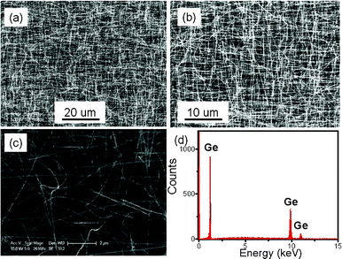 | ||
| Fig. 1 (a–c) SEM images of the GeNWs at different magnification. (d) The corresponding EDX spectrum. | ||
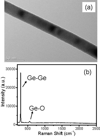 | ||
| Fig. 2 (a) A TEM image of a typical GeNW. (b) The Raman spectrum of GeNWs showing the presence of both Ge and Ge oxide. | ||
Fig. 3(a) shows the typical I–V curves of a single GeNW acquired from both two-probe and four-probe approaches. The linear curves throughout the voltage measurement range reveal the good ohmic contact between the electrodes and GeNW. The resistance of the NW is calculated to be 8.9 × 10⁶ Ω and the contact resistance, namely the difference between the two-probe and four-probe resistance is 4.1 × 10⁴ Ω. In light of the relatively low contact resistance, probably due to the matched work function,22 a two-probe method is used in the following experiments. The inset in Fig. 3(b) shows a typical FESEM image of the GeNW FET after 20 nm MoO3 deposition, in which two parallel gold electrodes are crossed by an individual GeNW. The effective gate length is 2.5 μm and the diameter of the NW is 80 nm. Fig. 3(b) plots Idsvs. Vds curves of a pure MoO3 thin layer and GeNW in air, at vacuum and after MoO3 coating. Among the four structures, MoO3 shows the lowest conductance, while the GeNW has higher conductance in air than when in a vacuum, mainly due to the ambient effect. Interestingly, after coating with a 20 nm MoO3 thin layer, the as-obtained GeNW/MoO3 structure shows the highest conductance. These results suggest that the substantial increase of the conductance for the MoO3-coated GeNW (GeNW/MoO3) cannot be solely attributed to the conductance enhancement of the MoO3 coating layer. As we will discuss later, the surface charge transfer between the MoO3 and GeNW interface is likely responsible for this phenomenon.
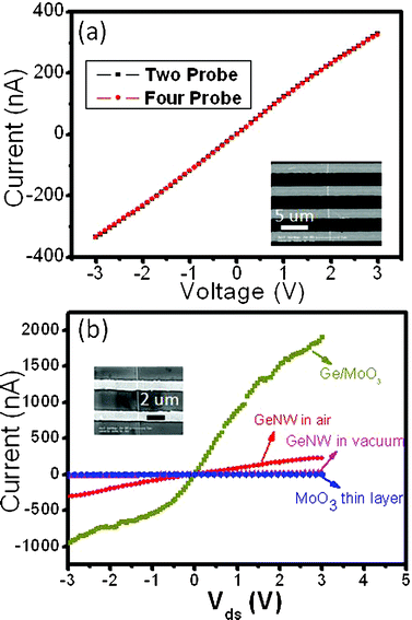 | ||
| Fig. 3 (a) I–V curves measured in both two-probe and four-probe configurations; inset shows four parallel Ti/Au electrodes bridged by an individual GeNW. (b) Conductance of GeNW in air, vacuum, GeNW coated with MoO3 (GeNW/MoO3), and MoO3 thin film, inset is the SEM image of a typical GeNW-FET. | ||
Further electrical transport characterization indicates that the undoped GeNWs without MoO3 coating shows weak p-type semiconductivity (data not shown). This behavior is attributed to the presence of a huge quantity of surface dangling bonds that can lead to the formation of an acceptor level slightly above the valance band maximum.23 In contrast, the p-type conductivity of the GeNW is remarkably enhanced after coating with MoO3 thin layer. Fig. 4(a) and (b) depict the transport characteristics of the GeNW FET after MoO3 coating. The device exhibits a typical behavior of a p-channel semiconductor FET, with a hole mobility and concentration of 45.3 cm2 V−1 s−1 and 5.8 × 1017 cm−3, respectively. A comparison of the hole mobility, hole concentration and resistivity of the GeNW in air, a vacuum and after MoO3 deposition is summarized in Fig. 4(c). It is worth noting that owing to oxygen and water molecules absorption on the surface dangling bonds, an acceptor level above the valence band was formed, contributing to the p-type conductivity of the GeNW in air. Desorption of these surface molecules in a vacuum leads to the decrease of the hole concentration. As a result, the resistivity of the GeNW increases by nearly one order of magnitude in a vacuum. On the other hand, the MoO3 coating on the GeNW results in the increase of both the hole mobility and the hole concentration. Consequently, the GeNW resistivity decreases by one order of magnitude with respect to that in air. The enhanced carrier mobility of GeNW after MoO3 coating is probably due to the reduced carrier scattering as a consequence of surface oxygen and water molecules desorption, as well as the effective surface passivassion.24,25 As for the increase in hole concentration, it is assumed to be associated with the mutual surface charge transfer between the GeNW and MoO3 thin layer due to their differences in work function, which will be verified by the in situ XPS analysis result later on.
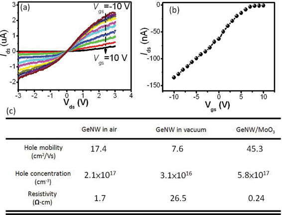 | ||
| Fig. 4 (a) Ids–Vds curve of GeNW after deposition of MoO3, under different gate voltages. (b) Corresponding transport characteristics at Vds= −0.1 V. (c) Table of electrical properties of GeNW in air, vacuum and with a layer of MoO3 thin film. | ||
Previously, it has been reported that MoO3 has a very low lowest unoccupied molecular orbital (LUMO) value of −6.7 eV and highest occupied molecular orbital (HOMO) value of −9.7 eV,26 signifying that the work function of MoO3 is comparatively larger than the majority of other materials including organic and inorganic semiconductors, thereby favoring holes injection from MoO3 to the other semiconductors, which render it an effective hole injector in organic LEDs and organic FETs.27,28 In our case, the huge difference in work functions between MoO3 and GeNW also accounts for the enhanced p-type conductivity in GeNW after MoO3 coating. As we can see in Fig. 5(a), the conduction band minimum (Ec) and the valence band maximum (Ev) of the GeNW are located at −3.6 and −4.3 eV, respectively. The Fermi level is above both the HOMO and LUMO of MoO3. As a result, electrons will transfer spontaneously from GeNW to MoO3 (Fig. 5(b)), giving rise to the increase in hole concentration within the GeNW. It is noteworthy that although an ultrathin GeO2 sheath is often observed on the outside of the GeNWs, it is too thin to block the electron transfer via direct tunneling. Moreover, similar electron transfer from GeO2 to MoO3 was also investigated in the XPS analysis below.
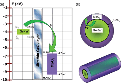 | ||
| Fig. 5 (a) A schematic illustration of the electron injection from GeNW to MoO3. (b) An electronic structures diagram of both GeNW and MoO3. | ||
As a matter of fact, the observed surface charge transfer doping effect was experimentally verified by XPS spectrum evolution of Ge 3d and Mo 3d with increasing nominal MoO3 coverage, as shown in Fig. 6(a). It can be clearly visualized that prior to MoO3 coating, the spectrum of Ge 3d is mainly composed of two Ge 3d peaks centered at binding energy of 29.84 and 33.32 eV, corresponding to Ge and GeO2, respectively. When the MoO3 thin layer is deposited stepwise, a gradual shift of Ge 3d towards low binding energy is observed for both peaks. Fig. 6(c) plots the binding energy shift as a function of MoO3 layer thickness, in which a total shift of about 0.43 eV for Ge and 0.42 eV for GeO2 is observed as MoO3 thickness increase from 0 to 10 nm. This binding energy shift corresponds to the upward energy level bending from bulk to interface, indicating that GeNW loses electrons near the heterojunction interface. The surface charge transfer effect at the GeNW/MoO3 interface is corroborated by the corresponding Mo 3d spectrum evolution as well. As shown in Fig. 6(b), with the increase in MoO3 thickness, the binding energy of Mo 3d shifts downwards by 0.33 eV; this shift suggests that the electrons were injected from the GeNW to MoO3, in good agreement with the enhanced p-type electrical conduction behavior.
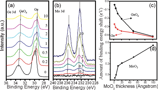 | ||
| Fig. 6 XPS spectra of Ge 3d (a) and Mo 3d (b) peaks for GeNWs coated with MoO3 of increasing thickness of 0, 0.2, 0.5, 1, 2, 5 and 10 nm. The binding energy shift of Ge 3d for GeNWs (c) and Mo 3d for MoO3 (d) with increasing MoO3 coverage. The shift of the binding energy confirms the surface charge transfer at the GeNWs and MoO3 interface. | ||
The charge transfer at the interface is also verified by the formation of an interface dipole. Fig. 7 plots the evolution of work function and VBM (i.e., the band bending) of MoO3 as a function of MoO3 layer thickness, from which one can see that as the dopant layer thickness increases from 0 to 100 Å, both the work function and VBM increase. Notably, a careful comparison of both values concludes that the change in work function is always larger than that of the band bending. This result suggests the existence of an interfacial dipole at the MoO3/GeNW interface, thus corroborating the electron transfer from GeNW to MoO3 at the contacting junction, considering the fact that the overall change in work function includes the contribution from both band bending and interfacial dipole.29,30
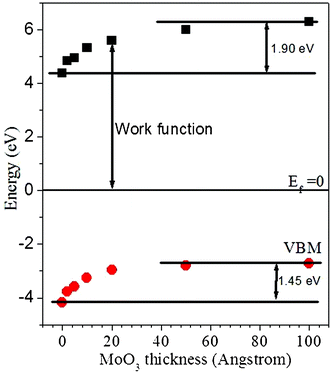 | ||
| Fig. 7 The energy level alignment of MoO3 as a function of increasing MoO3 thickness. | ||
It is worth mentioning that the MoO3 thin layer can not only serve as an effective hole injector, but also help prevent the GeNWs from getting oxidized when exposed in ambient conditions, which is often observed on GeNWs and responsible for the degeneration of their electrical properties.31 As depicted in Fig. 8(a), the GeNW without MoO3 thin layer coverage can get easily oxidized and its electrical conduction attenuates at a considerable pace in less than 1 week. However, the deposition of a MoO3 thin layer can act as a protective layer and greatly restrict such an oxidization process. Fig. 8(b) shows the hole mobility and the hole concentration of a 20 nm MoO3-coated GeNW FET as a function of exposure duration, from which one can see that the hole mobility decreases slightly from 45.3 to 44.5 cm2 V−1 s−1, and hole concentration decreases slightly from 5.75 × 10¹⁷ to 5.72 × 1017 cm−3 after storage in air for 3 months. The change in the device parameters is less than 2%, which unambiguously demonstrates that the GeNWs embedded in the MoO3 thin layer are extremely stable, greatly facilitating their applications in future nanoelectronic devices.
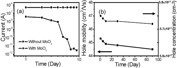 | ||
| Fig. 8 (a) Current evolution of a GeNW with and without MoO3 thin film deposition. (b) Hole mobility and concentration evolution of the MoO3-coated GeNW as a function of time. | ||
In summary, we have presented a surface transfer approach to the effective p-type doping of GeNWs via MoO3 thin film coating. The GeNWs studied were prepared by a conventional thermal evaporation approach. The electrical property study of the single GeNW-based field effect transistor and in situ XPS analysis of GeNWs as a function of increasing MoO3 coverage support the supposition that a considerable quantity of holes was transferred from MoO3 to GeNWs due to their difference in work function. Finally, the long-term electrical property study of the GeNW reveals that the hole mobility and concentration remain almost the same. The generality of this work demonstrates that surface transfer doping is an effective method to tailor the electrical property of GeNWs.
Acknowledgements
This work was supported by the National Natural Science Foundation of China (Nos.60806028, 61106010, 21101051, 20901021), the Program for New Century Excellent Talents in University of the Chinese Ministry of Education (NCET-08-0764), the Major Research Plan of the National Natural Science Foundation of China (No. 91027021) and the Fundamental Research Funds for the Central Universities.References
- J. Golberger, A. I. Hochbaum, R. Fan and P. D. Yang, Nano Lett., 2006, 6, 973–977 CrossRef.
- Y. Cui, Z. Zhong, D. Wang, W. U. Wang and C. M. Lieber, Nano Lett., 2003, 3, 149–152 CrossRef CAS.
- Y. Huang, X. F. Duan, Y. Cui, L. J. Lauhon, K. H. Kim and C. M. Lieber, Science, 2001, 294, 1313–1317 CrossRef CAS.
- W. I. Park, J. S. Kim and H. J. Lee, Nano Lett., 2005, 17, 1393–1397 CAS.
- X. F. Duan, Y. Huang, R. Agarwal and C. M. Lieber, Nature, 2003, 421, 241–245 CrossRef CAS.
- Y. Huang, X. F. Duan and C. M. Lieber, Small, 2005, 1, 142–147 CrossRef CAS.
- T. J. Kempa, B. Z. Tian, D. R. Kim, J. S. Hu, X. L. Zheng and C. M. Lieber, Nano Lett., 2008, 8, 3456–3460 CrossRef CAS.
- M. Zukalova, A. Zukal, L. Kavan, M. K. Nazeeruddin, P. Liska and M. Gratzel, Nano Lett., 2005, 5, 1789–1792 CrossRef CAS.
- L. Rigutti, M. Tchernycheva, A. D. Bugallo, G. Jacopin, F. H. Julien, L. F. Zagonel, K. March, O. Stephan, M. Kociak and R. Songmuang, Nano Lett., 2010, 10, 2939–2943 CrossRef CAS.
- L. B. Luo, J. S. Jie, Z. H. Chen, X. J. Zhang, X. Fan, G. D. Yuan, Z. B. He, W. F. Zhang, W. J. Zhang and S. T. Lee, J. Nanosci. Nanotech., 2009, 9, 6298–7304 Search PubMed.
- Y. Cui, Q. Q. Wei, H. K. Park and C. M. Lieber, Science, 2001, 293, 1289–1292 CrossRef CAS.
- L. B. Luo, J. S. Jie, W. F. Zhang, Z. B. He, J. X. Wang, G. D. Yuan, W. J. Zhang, L. C. M. Wu and S. T. Lee, Appl. Phys. Lett., 2009, 94, 193101–3 CrossRef.
- B. S. Kim, T. W. Koo, J. H. Lee, D. S. Kim, Y. C. Jun, S. W. Hwang, B. L. Choi, E. K. Lee, J. M. Kim and D. M. Whang, Nano Lett., 2009, 9, 864–869 CrossRef CAS.
- P. Nguyen, H. T. Ng and M. Meyyappan, Adv. Mater., 2005, 17, 549–553 CrossRef CAS.
- P. Logan and X. H. Peng, Phys. Rev. B, 2009, 80, 115322 CrossRef.
- R. P. Prasankumar, S. Choi, S. A. Trugman, S. T. Picraux and A. J. Taylor, Nano Lett., 2008, 8, 1619–1624 CrossRef.
- S. J. Sze, Physics of Semiconductor Devices, 2nd ed. 1981, Wiley, New York Search PubMed.
- X. Y. Wu, J. S. Kulkarni, G. Collins, N. Petkov, D. Almecija, J. J. Boland, D. Erts and J. D. Holmes, Chem. Mater., 2008, 20, 5954–5967 CrossRef CAS.
- J. Ristein, Science, 2006, 313, 1057–1058 CrossRef CAS.
- D. W. Wang, Y. L. Chang, Z. Liu and H. J. Dai, J. Am. Chem. Soc., 2005, 127, 11871–11875 CrossRef CAS.
- N. Fukata, K. Sato, M. Mitome, Y. Bando, T. Sekiguchi, M. Kirkham, J. I. Hong, Z. L. Wang and R. L. Snyder, ACS Nano, 2010, 4, 3807–3816 CrossRef CAS.
- Q. X. Tang, Y. H. Tong, W. P. Hu, Q. Wan and T. Bjornholm, Adv. Mater., 2010, 21, 4234–4237 CrossRef.
- L. B. Luo, X. B. Yang, F. X. Liang, J. S. Jie, C. Y. Wu, L. Wang, Y. Q. Yu and Z. F. Zhu, J. Phys. Chem. C, 2011, 115, 24293–24299 CAS.
- C. S. Guo, L. B. Luo, G. D. Yuan, X. B. Yang, R. Q. Zhang, W. J. Zhang and S. T. Lee, Angew. Chem., Int. Ed., 2009, 48, 9896–9900 CrossRef CAS.
- J. S. Jie, W. J. Zhang, K. Q. Peng, G. D. Yuan, C. S. Lee and S. T. Lee, Adv. Funct. Mater., 2008, 18, 3251–3257 CrossRef CAS.
- M. Kroger, S. Hamwi, J. Meyer, T. Riedl, W. Kowalsky and A. Kahn, Org. Electron., 2009, 10, 932–938 CrossRef CAS.
- J. Meyer, R. Khalandovsky, P. Gorrn and A. Kahn, Adv. Mater., 2011, 23, 70–73 CrossRef CAS.
- H. B. Wang, Z. T. Liu, M. F. Lo, T. W. Ng, C. S. Lee, D. H. Yan and S. T. Lee, J. Appl. Phys., 2010, 107, 024510–3 CrossRef.
- H. Ishiii, K. Sugiyama, E. Ito and K. Seki, Adv. Mater., 1999, 11, 605 CrossRef.
- D. C. Qi, W. Chen, X. Y. Gao, L. Wang, S. Chen, K. P. Loh and A. T. S. Wee, J. Am. Chem. Soc., 2007, 129, 8084 CrossRef CAS.
- R. H. Kinston, Semiconductor Surface Physics, University of Pennsylvania Press, Philadelphia, 1957 Search PubMed.
| This journal is © The Royal Society of Chemistry 2012 |