Large scale two-dimensional nanobowl array high efficiency polymer solar cell†
Szu-Ying
Chen
a,
Yu-Ting
Yen
a,
Yi-Yang
Chen
b,
Chain-Shu
Hsu
b,
Yu-Lun
Chueh
*a and
Lih-Juann
Chen
*a
aDepartment of Materials Science and Engineering, National Tsing Hua University, Hsinchu, 30013, Taiwan, R.O.C.. E-mail: ylchueh@mx.nthu.edu.tw; ljchen@mx.nthu.edu.tw; Tel: +886-5715131-33965
bDepartment of Applied Chemistry, National Chiao-Tung Univerisy, 1001 University Road, Hsinchu, Taiwan 300, ROC
First published on 6th January 2012
Abstract
A two-dimensional nanobowl array (2D-NBRs) with a unique honeycomb nanostructure was demonstrated with controllable morphologies synthesized by the Langmuir–Blodgett (LB) method. The periodicity of 2D-NBRs can be controlled by utilizing different diameters of polystyrene (PS) balls ranged from 500 nm, 870 nm, 1 μm to 2 μm. The reflectance measurements revealed that the planar structure with a poly(3-hexylthiophene) (P3HT)/(6,6)-phenyl-C61-butyric acid methyl ester (PCBM) bulk heterojunction layer as an active layer exhibits a reflectance of ∼20 %, while a significant reduction of the reflectance <5–7 % can be achieved after formation of 2D-NBRs at a PS ball diameter of 500 nm, which perfectly matches simulation results. From experimental results, the highest efficiency of 5.4 % with a filling factor of 66 % was achieved for the device with 2D-NBRs at PS ball diameter of 870 nm. Compared to a planar device with an efficiency of 3.9 %, a maximum enhancement of ∼40 % can be achieved owing to the enhancement of Jsc because of unique honeycomb geometry, which exhibits a broadband and omnidirectional light harvesting behavior. Furthermore, a flexible solar cell was demonstrated with an enhanced efficiency of 30 % for a planar structure of 1 % to 1.3 % for 2D-NBRs structure.
Introduction
Organic photovoltaics (OPV) have attracted much attention due to many advantages, including low-cost, renewable energy conversion, and large area with printable processes.1–3 A typical configuration of an organic photovoltaic consists of a single bulk-heterojunction active layer, which is combined with polythiophene derivatives as a donor layer and fullerenes as an acceptor layer. This active layer is spontaneously phase-separated into interconnected domains. Under illumination, electron-hole pairs, generated between the donor and the acceptor layers, are transported through the interconnected domains, resulting in a photocurrent for energy harvesting.4,5 Owing to its disordered nature, including (i) insufficient carrier separation because of very small diffusion length of the excitons (<15 nm)6 and (ii) lack of sufficient light absorption ability, the power conversion efficiency (PCE) of the bulk-heterojunction system is still far away from routine demand.7–9 Therefore, the improvement of the power conversion efficiency is an urgent goal for the design of a new polymer-based photovoltaic (PV) cell.To tackle these issues in order to boost the PCE, many methods have been adopted, including thermal annealing of solvent, optimization of solvent, compositional adjustment of active layer, and surficial patterning of active layer. Particularly, the control of surface morphology is critically important and can enhance the charge transfer, thus preventing recombination of the electrons and holes.10–15 Conventionally, the nanostructured organic photovoltaics employ molds with ordered structures viacontact printing process while they require much effort to create pattern with much higher degree of order in nanoscale, which limits the area of the patterned region.
In this study, we use the Langmuir–Blodgett (LB) method to form two-dimensional nanobowl arrays (2D-NBRs) with honeycomb nanostructure by assembling the closely packed polymer nanoparticles array on an ITO/glass substrate. The periodicity of nanobowls can be controlled by utilizing different diameters of polystyrene (PS) balls from 500 nm, 870 nm, 1 μm to 2 μm, respectively. The method provides an effective way as a template to achieve a largely patterned area of active layer with controllable morphologies from nano-to micro-meters.
Results and discussion
As shown in Fig. 1(a) the samples were etched by O2-plasma for 40 s to separate each PS ball, as shown in Fig. 1(b). The second ITO layer with a thickness of 250 nm was deposited upon the PS balls (Fig. 1c) and the samples were then dipped into toluene to remove the PS balls (lift-off process). Consequently, ITO with 2D-NBRs can be formed as shown in Fig. 1d. The optical and SEM images of 2D-NBRs are shown in Fig. 1(e) and inset, respectively, confirming the highly ordered and monolayer features. Interestingly, the density of these 2D-NBRs is controllable, depending on different diameters of PS balls, which are from 500 nm, 870 nm, 1 μm, and 2 μm as shown in Fig. 1(f), respectively. The smaller the diameter of the PS balls, the higher the density of 2D-NBRs can be achieved while the aspect ratio, defined as the ITO thickness divided by distance between each PS ball, decreases with an increasing diameter of PS ball at an identical ITO thickness of 250 nm.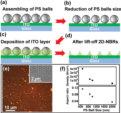 | ||
| Fig. 1 (a)–(d) Schematic illustrations of the preparation of 2D NBRs on ITO/glass substrate. (e) Scanning electron microscopy (SEM) and optical microscopy images of 2D-NBRs. (f) Density and aspect ratio as a function of PS ball diameter. | ||
To characterize the properties of antireflection and light trapping on these ITO 2D-NBRs with different periodicity caused by the different diameter of PS ball, the PEDOT:PSS/(3-hexylthiophene)(P3HT)/(6,6)-phenyl-C61-butyric acid methyl ester (PCBM) bulk heterojunction active layer was prepared by spin-coating process on top of ITO 2D-NBRs with a thicknesses of 200 nm. The reflectance measurement was conducted by standard hemispherical reflection measurements over broad wavelengths ranged from 300–800 nm, which cover most of the solar spectrum. For comparison, the reflectance of the bulk heterojunction active layer on the ITO thin film (TF) was also measured. Fig. 2(a) shows the full reflectance of bulk heterojunction active layer on ITO TF and various periodic ITO 2D-NBRs synthesized with PS balls of different diameters. The bulk heterojunction active layer on ITO TF shows the reflectance of ∼20 % while the significant reduction of reflectance to ∼5–7 % can be achieved for heterojunction active layer on ITO 2D-NBRs, depending on the periodicity of the pattern. The reflectance decreases as the diameter of PS ball decreases, namely, smaller interspacing of ITO 2D-NBRs. As a result, the minimum reflectance can be achieved as diameter of PS ball is of 500 nm in the present study. The observed reflective behavior is attributed to a concept of gradual refractive index that has been theoretically and experimentally demonstrated by several research groups.16,17 Accordingly, the large Fresnel reflection observed on ITO TF is due to the different refractive index mismatch between the air (n = 1) and ITO (n = 2.3272–1.6556 at 300 to 800 nm). The low reflectance behavior of the heterojunction active layer on the ITO 2D-NBRs is resulted from its unique geometry, an effective geometry for antireflection and enhancement of absorption ability with refractive index matching better with air, thereby providing a smooth transition of refractive index from the top to the base of 2D-NBRs.
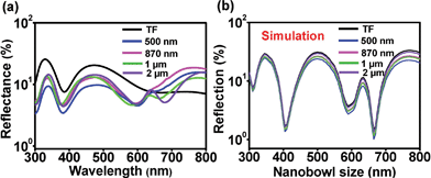 | ||
| Fig. 2 (a) Reflectance spectra of 2D-NBRs with different PS ball diameters. (b) Simulated reflectance spectra of 2D-NRs with different PS ball diameters. | ||
Furthermore, the simulation of reflectance for the 2D-NBRs with different periodicity varying with the diameter of PS ball was performed using TCAD as shown in Fig. 2(b) in order to precisely predict the reflectance behavior. The simulation of the reflection curves were conducted by Sentaurus TCAD version D-2010.03 with optical solver “raytracer”. The simplified 2D structure and the simulation unit cell are shown in Figure S1, ESI.† The surface was assumed to have triangle protrusions after sputtering of ITO layer with layer structures of ITO/PEDOT:PSS/P3HT-PCBM. (Figure S1) The active layer with a thickness of 200 nm was assumed over the surface. The n and k values for ITO layer were independently measured by ellipsometry while the P3HT-PCBM layer is from ref. 18. As can be seen from Fig. 2(b), the minimum reflectance can be achieved as the diameter of PS ball is of 500 nm, which fully agrees with the experimental results.
Nanostructured devices have been shown to possess a refractive index matching with air that significantly suppresses light reflection larger than pristine devices over the whole spectrum.19–23 To shed light on how the 2D-NBRs can be used effectively for organic solar cell to boost the device efficiency, Ca/Al with thickness of 35/100 nm was prepared as conducting electrodes on active layers with ITO TF and 2D-NBRs nanostructures, which is schematically illustrated in Fig. 3(a) and (b). Insets in Fig. 3(a) and (b) show the atomic force microscopy (AFM) images after the coating of the active layer. The solar efficiency and external quantum efficiency (EQE) was measured using Keitheley 4200 under illumination of AM 1.5 (100 mW cm−2) using solar simulator at room temperature. Fig. 3(c) shows the I–V behavior of planar and 2D-NBRs structures with different diameters of PS balls under the illumination of AM 1.5. The corresponding short circuit current (JSC), open circuit voltage (VOC), filling factor (FF), and power conversion efficiency (PCE) are listed in Table 1 and plotted in Fig. 3(d) and (e) for devices with planar structure and 2D-NBRs prepared with PS balls of different diameters. The planar device yields a JSC of 10.73 mA cm−2 with a VOC of 600 mV while an enhanced JSC of 2D-NBRs can be achieved from 10.73 to the highest value of 13.08 mA cm−2 prepared with a PS ball diameter of 870 nm with the same VOC at 600 mV. On the other hand, a decrease of JSC can be found once the diameter of the PS ball was larger than 1 μm while VOC remains ∼600 (mV). Thus, after the formation of 2D-NBRs, the highest efficiency and filling factor of 5.4 % and 66 %, respectively, were achieved in devices fabricated with PS balls of a diameter of 870 nm, while the efficiency decreases when the diameter of the PS ball was 1 μm or larger, which shows the same trend as the JSC. Compared to a planar device, an enhancement of ∼40 % can be achieved after the formation of 2D-NBRs with PS balls with a diameter of ∼870 nm, which is mainly due to the enhancement in JSC.
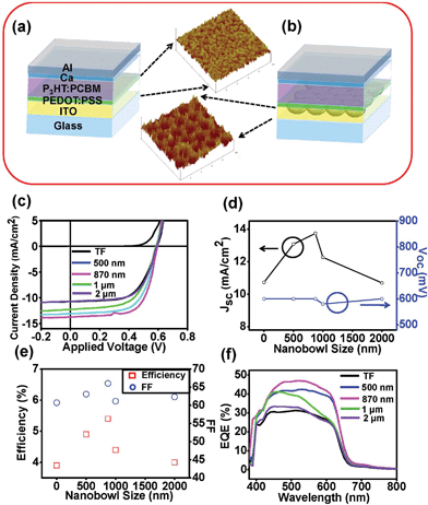 | ||
| Fig. 3 (a) And (b) show schematics of conventional planar and 2D-NBRs devices. Insets show the surface morphologies taken with an atomic force microscope. (c) The I–V results for devices with planar and 2D-NBRs with different PS ball diameters measured under illumination of AM 1.5 with a light intensity of 100 mW cm−2. (d)–(f) Short-circuit current density (JSC), open circuit voltage (VOC), power conversion efficiency (PCE), filling factor (FF), and external quantum efficiency (EQE) as a function of different PS ball diameter. | ||
| PS ball size | Jsc (mA cm−2) | Voc (mA) | FF(%) | η (%) |
|---|---|---|---|---|
| TF | 10.73 | 600 | 60.7 | 3.9 |
| 500 nm | 13.08 | 600 | 63.1 | 4.9 |
| 870 nm | 13.74 | 600 | 66.0 | 5.4 |
| 1 μm | 12.27 | 580 | 61.1 | 4.4 |
| 2 μm | 10.69 | 600 | 62.3 | 4.0 |
Photocurrent generation is principally governed by three major factors, including the number of absorbed photons, the number of carriers generated by charge separation at interfaces between donor and acceptor, and the charge-collection efficiency.24 Therefore, the enhanced JSC is ascribed to the increase in photocurrent owing to the higher electron-hole pair generation resulted from the higher light trapping behavior because of the unique honeycomb geometry, which effectively matches the refractive index with that of air. In addition, the enlarged contact area between active layer and electrode after the formation of the 2D-NBRs also improves the efficiency of carrier collection and transportation. However, the enlarged area may also lead to a higher contact resistance to degrade the device performance. The combined effects can explain why 2D-NBRs prepared with PS balls of 870 nm diameter exhibit the highest enhancement of JSC and efficiency. The external quantum efficiency (EQE) was measured using Keitheley 4200 under the solar simulator of AM 1.5 (100 mW cm−2) at room temperature. The differences in external quantum efficiency provide the information of generated carriers and charge collection efficiency. The EQE was found to increase with increasing PS ball diameter first then decrease as the diameter of PS ball exceeds 1 μm. The increased EQE response from wavelengths of 400 to 650 nm can be attributed to the increase in electron-hole pairs (EHPs) concentrations owing to a broadband and omnidirectional light harvesting behavior, thereby enhancing JSC and FF. Again, the maximum EQE can be achieved with PS ball diameter of ∼870 nm.
One of the main advantages of organic solar cells is their low temperature process, which can be adopted into processes of flexible solar panels as a promising new breed of solar devices in desirable size and shape owing to a very exceptional space efficiency. In addition, the active materials used for the fabrication of devices are soluble in the most common organic solvents, enabling the manufacture of polymer solar cell by roll-to-roll printing processes. To achieve this, we transferred 2D-NBRs onto a PET substrate, which is one of the flexible substrates to demonstrate the feasibility of flexible nanostructured solar cells. Here, we used a diameter of PS ball ∼870 nm to form the ITO 2D-NBRs on PET substrate, which can achieve the highest efficiency. The corresponding I–V behavior under the illumination of AM 1.5 is shown in Fig. 4. The optical image of the 2D-NBRs flexible device is shown in the inset of Fig. 4. The device shows a JSC of 7.01 mA cm−2 with a VOC of 560 mV, yielding a η of 1 % with a FF of 27.1 %, while an increase of JSC after the formation of 2D-NBRs from 7.01 to 9.03 mA cm−2 can be achieved with an improved η and FF of 1.3 % and 27.4 %, respectively. The scheme provides an effective means to use an appropriate template with large patterned area of active layer and controlled morphologies.
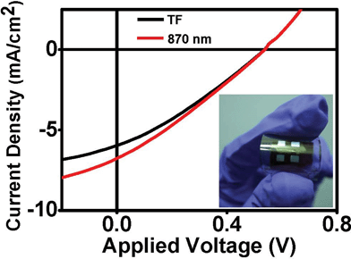 | ||
| Fig. 4 I–V behaviors of flexible devices based on planar and 2D-NBRs structures under illumination of 1.5 AM. The results demonstrated the feasibility of 2D-NBRs on flexible substrate (PET). Inset shows the optical image of the flexible device. | ||
Conclusions
In summary, two-dimensional nanobowl arrays (2D-NBRs) with honeycomb nanostructure were demonstrated by assembling the closely packed polymer nanoparticles array on ITO/glass substrate by the Langmuir–Blodgett (LB) method. The periodicity of the nanobowls can be controlled by utilizing different diameters of polystyrene (PS) balls (500 nm, 870 nm, 1 μm and 2 μm). The PEDOT:PSS/(3-hexylthiophene)(P3HT)/(6,6)-phenyl-C61-butyric acid methyl ester (PCBM) bulk heterojunction active layer on ITO TF shows the reflectance of ∼20 % while a significant reduction of reflectance into ∼5–7 % can be achieved for ITO 2D-NBRs. The efficiency after formation of ITO 2D-NBRs yields the highest efficiency and filling factor of 5.4 % and 66 % with PS ball diameter of 870 nm while the efficiency decreases as the diameter of PS ball exceeds 1 μm. Compared to a planar device with an efficiency of 3.9 %, an enhancement of ∼40 % can be achieved after the formation of 2D-NBRs with a PS ball diameter of ∼870 nm, which is mainly due to the enhancement in JSC due to a broadband and omnidirectional light harvesting behavior because of the unique honeycomb geometry. Furthermore, the 2D-NBRs on flexible substrate was demonstrated with an enhancement of 30 % in efficiency.Experimental section
Preparation of 2D-NBRs transparent electrodes
We used the Langmuir–Blodgett (LB) assembly method to form two-dimensional nanobowl arrays (2D-NBRs) with honeycomb nanostructures by assembling the close packed polymer nanoparticles array on ITO/glass substrate. The scheme provides an effective means to use an appropriate template with large patterned area of active layer and controlled morphologies. The periodic array of nanobowls can be controlled by utilizing different diameters of polystyrene (PS) balls from 500 nm, 870 nm, 1 μm to 2 μm.Device fabrications
ITO with 2D-NBRs substrates were cleaned by ultrasonic treatment in acetone and isopropyl solvents. The ITO 2D-NBRs glass was then subjected to O2-plasma treatment. A thin layer of the PEDOT:PSS film was spin-coated onto ITO 2D-NBRs with a speed of 400 rpm for 3 s and 4000 rpm for 40 s, respectively. The samples were dried on a hot plate at 120 °C for 20 min and then transferred in a nitrogen-filled glove-box for spin-coating a P3HT:PCBM photoactive layer at the speed of 600 rpm for 30 s followed by 1200 rpm for 3 s. The P3HT:PCBM (1![[thin space (1/6-em)]](https://www.rsc.org/images/entities/char_2009.gif) :1, w/w) blend solution was prepared in dichlorobenzene solvent and stirred for 24 h under N2 conditions. The Ca (35 nm) and Al (150 nm) layers were thermally evaporated through a shadow mask with an active area of ∼0.4 cm2.
:1, w/w) blend solution was prepared in dichlorobenzene solvent and stirred for 24 h under N2 conditions. The Ca (35 nm) and Al (150 nm) layers were thermally evaporated through a shadow mask with an active area of ∼0.4 cm2.
Morphology characterizations
The surface morphology and the roughness of the 2D-NBRs substrate were determined with a Digital Instruments Nanoscope 3100 atomic force microscope (AFM, Veeco DI 3100) and field-emission scanning electron microscope (FE-SEM, JEOL 6500F).Measurements and characterizations
All electrical measurements were performed in a glove box with nitrogen ambient at room temperature. The current–density–voltage (J–V) characteristics were measured with an Keithley 4200 system under solar simulator of A.M. 1.5 at 100 mW cm−2 (1 sun). UV-Visible absorption spectra were obtained using a HITACHI U4100 spectrophotometer.Acknowledgements
The research was supported by the National Science Council through grant no. NSC 99-2628-E-007-003-, NSC 98-2112-M-007-025-MY3, and NSC 98-2221-E-007-104-MY3.References
- C. J. Brabec, Sol. Energy Mater. Sol. Cells, 2004, 83, 273 CrossRef CAS.
- F. C. Krebs, Sol .Energy Mater. Sol. Cells, 2009, 93 Search PubMed.
- R. Gaudiana and C. J. Brabec, Nat. Photonics, 2008, 2, 287 CrossRef CAS.
- S. H. Park, A. Roy, S. Beaupré, S. Cho, N. Coates, J. S. Moon, D. Moses, M. Leclerc, K. Lee and A. J. Heeger, Nat. Photonics, 2009, 3, 297 CrossRef CAS.
- Y. Y. Liang, D. Q. Feng, Y. Wu, S. T. Tsai, G. Li, C. Ray and L. P. Yu, J. Am. Chem. Soc., 2009, 131, 7792 CrossRef CAS.
- P. E.Shaw, A. Ruseckas and I. D. W. Samuel, Adv. Mater., 2008, 20, 3516 CrossRef.
- S. R. Forrest, MRS Bull., 2005, 30, 28 CrossRef CAS.
- K. M. Coakley, Y. Liu, C. Goh and M. D. McGehee, MRS Bull., 2005, 30, 37–40 CrossRef CAS.
- G. Lu, L. Li and X. Yang, Small, 2008, 4, 601 CrossRef CAS.
- W. Ma, C. Yang, X. Gong, K. Lee and A. J. Heeger, Adv. Funct. Mater., 2005, 15, 1617 CrossRef CAS.
- X. Yang, G. Lu, L. Li and E. Zhou, Small, 2007, 3, 611 CrossRef CAS.
- G. Li, Y. Yao, H. Yang, V. Shrotriya, G. Yang and Y. Yang, Adv. Funct. Mater., 2007, 17, 1636 CrossRef CAS.
- G. Li, V. Shrotriya, J. Huang, Y. Yao, T. Moriarty, K. Emery and Y. Yang, Nat. Mater., 2005, 4, 864 CrossRef CAS.
- J. M. Kroon, M. M. Wienk, W. J. H. Verhees and J. C. Hummelen, Thin Solid Films, 2002, 403, 223 CrossRef.
- F. C. Chen, Y. K. Lin and C. J. Ko, Appl. Phys. Lett., 2008, 92, 023307 CrossRef.
- J. Q. Xi, M. F. Schubert, J. K. Kim, E. F. Schubert, M. Chen, S. Y. Lin, W. Liu and J. A. Smart, Nat Photon, 2007, 1, 176 CAS.
- Y. F. Huang, S. Chattopadhyay, Y. J. Jen, C. Y. Peng, T. A. Liu, Y. K. Hsu, C. L. Pan, H. C. Lo, C. H. Hsu, Y. H. Chang, Y. K. Hsu, C. L. Pan, H. C. Lo, C. H. Hsu, Y. H. Chang, C. S. Lee, K. H. Chen and L. C. Chen, Nat. Nanotechnol., 2007, 2, 770 CrossRef CAS.
- F. Monestier, J. J. Simon, P. Torchio, L. Escoubas, F. Flory, S. Bailly, R. de Bettingnies, S. Guillerez and C. Defranoux, Sol. Energy Mater. Sol. Cells, 2007, 91, 405 CrossRef CAS.
- Y. F. Huang, S. Chattopadhyay, Y. J. Jen, C. Y. Peng, T. A. Liu, Y. K. Hsu, C. L. Pan, H. C. Lo, C. H. Hsu, Y. H. Chang, C. S. Lee, K. H. Chen and L. C. Chen, Nat. Nanotechnol., 2007, 2, 770 CrossRef CAS.
- Y. J. Lee, D. S. Ruby, D. W. Peters, B. B. McKenzie and J. W. P. Hsu, Nano Lett., 2008, 8, 1501 CrossRef CAS.
- T. Lohmuller, M. Helgert, M. Sundermann, R. Brunner and J. P. Spatz, Nano Lett., 2008, 8, 1429 CrossRef.
- J. Zhu, Z. Yu, G. F. Burkhard, C. M. Hsu, S. T. Connor, Y. Xu, Q. Wang, M. McGehee, S. Fan and Y. Cui, Nano Lett., 2009, 9, 279 CrossRef CAS.
- Z. Yu, H. Gao, H. Wu, H. Ge and S. Y. Chou, J. Vac. Sci. Technol. B, 2003, 21, 3974 Search PubMed.
- G. Yu, J. Gao, J. C. Hummelen, F. Wudl and A. J. Heeger, Science, 1995, 270, 1789 CAS.
Footnote |
| † Electronic supplementary information (ESI) available: schematic 2D-NBRs for simulation. See DOI: 10.1039/c2ra01258h |
| This journal is © The Royal Society of Chemistry 2012 |