Anisotropic etching of microscale β-FeSi2 particles: Formation, mechanism, and quantum confinement of β-FeSi2 nanowhiskers
J. Y.
He
a,
X.
Wang
a,
X. L
Wu
*a and
Paul K.
Chu
b
aNanjing National Laboratory of Microstructures and Department of Physics, Nanjing University, Nanjing, 210093, China. E-mail: hkxlwu@nju.edu.cn; Fax: +86-25-83595535; Tel: +86-25-83686303
bDepartment of Physics and Materials Science, City University of Hong Kong, Tat Chee Avenue, Kowloon, Hong Kong, China
First published on 2nd March 2012
Abstract
Needle-shaped β-FeSi2 nanowhiskers with diameters of 1–5 nm and lengths of 20–100 nm are produced by chemical etching of β-FeSi2 powders with microscale particles. The nanowhiskers mainly exhibit a <400> growth direction due to the anisotropic etching following the lowest etching rate of the Fe atomic facets. The absorbance spectra show that the energy gap of the β-FeSi2 nanowhiskers increases from 0.81 (bulk) to 0.94 eV, demonstrating distinct quantum size effect.
Beta-phase iron silicide (β-FeSi2) is an environmentally friendly semiconductor possessing many unique physical and chemical properties with applications in near infrared detectors, light emitters and solar cells.1–10 With the rapid development of nanotechnology, β-FeSi2 has spurred renewed interest in recent years.8,9 A range of techniques such as ion beam synthesis, reactive deposition epitaxy, magnetron sputtering, pulsed laser deposition, and molecular beam epitaxy have been employed to fabricate iron silicide nanomaterials11–14 and most of the studies have focused on the fabrication of nano-structured films. In these methods, rigorous experimental conditions such as sophisticated instruments and complicated pre-separation steps are required. Moreover, it is quite difficult to fabricate nanostructures with diameters smaller than the Bohr radius, especially one-dimensional nanostructures. Hence, an economical, effective and easily controlled method needs to be explored for synthesis of the β-FeSi2 nanostructures and a demonstration of the quantum size effect.
Wet chemical etching, which is based on the oxidation of materials in an alkaline or acidic medium, is commonly practiced in microelectronic processing and the fabrication of nanocrystals (NCs).15,16 Although iron silicide does not react with alkali and most acids, it reacts with hydrofluoric acid. Here, we report for the first time a simple chemical etching route to synthesize bulk quantities of β-FeSi2 nanowhiskers from powders. The nanowhiskers have diameters smaller than 5 nm and lengths between 20–100 nm. Based on the microstructural observations and spectral analysis, we reveal the formation mechanisms and quantum confinement effect of the nanowhiskers.
2.0 g β-FeSi2 powders with grain sizes of several to tens of micrometers were used as the precursors. The acid for electroless etching contained 50 mL of 99.7% ethanol (CH3CH2OH) and 5 mL of 40% hydrofluoric acid (HF). The reaction is: FeSi2 + HF → FeF2 + SiF4 + H2, where SiF4 and H2 are gases and FeF2 is a solid which is insoluble in water. In the reaction, HF acts as the oxidizing agent and partially dissolves β-FeSi2 to form interconnected nanostructure networks. In order to remove FeF2 we first added NaOH, and the reaction product of FeF2 with NaOH was Fe(OH)2, which was also water insoluble. Finally, enough HNO3 was added to produce highly soluble Fe(NO3)2. The overall reaction is: FeF2 + 2Na(OH) → Fe(OH)2 + 2NaF and Fe(OH)2 + 2HNO3 → Fe(NO3)2 + 2H2O.
The β-FeSi2 powders were etched for 30 min. Afterwards, the solution was centrifuged at 8000 rpm for 5 min to remove excess acid and salts. The resulting powders were washed with de-ionized water and dried at 70 °C for several hours. The residual powder weighed about 1 g and the etching rate was estimated to be about 2 g h−1. Ethanol was then added, followed by ultrasonic treatment for 30 min. The ultrasonic frequency and power were 40 kHz and 150 W, respectively. The ethanol solution with the suspended powder was left undisturbed for over 12 h and then centrifuged at 8000 rpm for 10 min. The supernate contained the β-FeSi2 NCs.
A drop of the treated supernate was put on a copper mesh coated with carbon. Fig. 1(a) shows the transmission electron microscopy (TEM) image of the β-FeSi2 NCs. The NCs show a nanowhisker-like morphology with diameters of 1–5 nm and lengths of 20–100 nm. Our selected area electron diffraction (SAED) pattern and energy-dispersive X-ray (EDX) spectra suggest that the nanowhisker-like NCs are not folded sheets with the dark regions corresponding to the folds. Instead, the sheet-like substance is shown to be some water traces which have not been evaporated completely before the TEM observations. The smallest β-FeSi2 NCs are only about 1 nm in diameter and are far smaller than the Bohr radius of β-FeSi2 (2.4 nm).17 This result means that the formation mechanism of these β-FeSi2 nanowhiskers is different from those of spherical Si and SiC NCs.16,18 A representative high-resolution TEM (HRTEM) image is depicted in Fig. 1(b). The lattice fringe spacing of 0.25 nm is in good agreement with that of the (400) plane of the beta-phase iron silicide. This implies that the nanowhiskers grow along the <400> direction and thus the etching rate along the <400> direction is much slower than those along other crystal directions. Fig. 1(c) shows the SAED pattern of the nanowhisker. The diffraction spots further confirm that the nanowhiskers are single crystalline β-FeSi2 with growth planes of (400), (202), and (020). The EDX spectrum in Fig. 1(d) indicates that the nanowhiskers are composed of Fe, Si and O, and the oxygen exists mainly in the surface layer. It is possible that the chemical etching makes the surfaces of the nanowhiskers terminated by oxygen to form Fe/Si oxide.
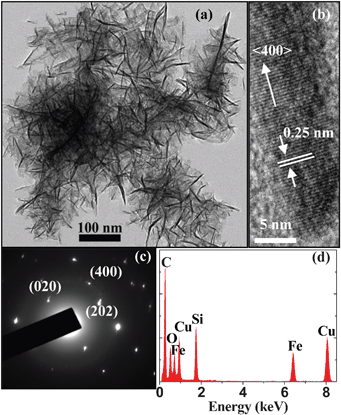 | ||
| Fig. 1 (a) TEM image of the β-FeSi2 nanowhiskers taken from the ethanol suspension. (b) HRTEM image of one nanowhisker. (c) SAED pattern and (d) EDX spectrum taken from one needle-shaped nanowhisker. | ||
To further determine the crystalline structure, the X-ray diffraction (XRD) and Raman spectra are presented in Fig. 2. The initial iron silicide powder with α- and β-phases was purchased from Alfa Company and then annealed at 840 °C in a vacuum of 10−4 Pa for 48 h. It is known that the transition temperature from β- to α-FeSi2 is at about 937 °C for the bulk phase. The XRD pattern (Fig. 2a) of the powder sample after annealing shows that the diffraction peaks are very consistent with those in the standard card of β-FeSi2 (Fig. 2b), indicating that the α-FeSi2 phase in the initial powder has completely transformed into the β-FeSi2 phase. The XRD pattern (Fig. 2c) of the nanowhiskers is consistent with Fig. 2a. The diffraction peaks can be indexed to reflections from the (202), (312), (331), (511) and (422) planes of β-FeSi2. Here, it should be mentioned that although the nanowhiskers mainly grow along the <400> direction, we do not observe reflection from the (400) plane because it is forbidden. The upper left inset in Fig. 2 displays the Raman spectrum of the nanowhiskers. There are 5 strong Raman peaks at 189, 196, 242, 277, and 333 cm−1 and their positions coincide well with those of β-FeSi2.19,20 These results reveal that chemical etching can produce high-quality crystalline β-FeSi2 nanowhiskers.
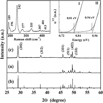 | ||
| Fig. 2 XRD patterns of (a) the initial microscale β-FeSi2 powder, (b) standard β-FeSi2 material (JCPDS card no. 71–0642), and (c) β-FeSi2 nanowhiskers. The upper-left inset shows the Raman spectrum of the nanowhiskers. The upper-right inset shows the absorbance spectra (T = 300 K) of the β-FeSi2 microscale powder (I) and nanowhiskers (II). | ||
To study the bang gap modification caused by size reduction, the absorbance spectra are shown in the upper right inset in Fig. 2. The band gap (absorption edge) of the microscale particles from the powders is 0.81 eV which is consistent with that reported previously.19,20 However, the band gap of the nanowhiskers is ∼0.94 eV which increased remarkably due to the quantum-confinement effect. Based on the obtained band gap (∼0.94 eV) of the nanowhiskers, the mean size of nanowhiskers is estimated to be about 4.1 nm, which is in good agreement with the observed size of the fabricated nanowhiskers.21,22 Hence, the existence of quantum confinement is clearly demonstrated.
To further explore the formation mechanism, the scanning electron microscopy (SEM) images of β-FeSi2 powder after chemical etching without ultrasonic treatment are shown in Fig. 3a. The surface morphology of the large β-FeSi2 grain is completely different from those of Si and SiC. After etching, the surface shows many parallel cuboid-like microrods. By calculating the lengths and diameters of the nanowhiskers, the ratio of the etching rates in the <400> and other orthorhombic directions is determined to be 1![[thin space (1/6-em)]](https://www.rsc.org/images/entities/char_2009.gif) :20. The lower left inset in Fig. 3(a) displays a magnified SEM image showing some nanowhiskers on the surface. In the TEM image, they look like nanorods. If the etching time is increased slightly, the nanorods become smaller, as shown in Fig. 1(a), because of the larger etching rate.
:20. The lower left inset in Fig. 3(a) displays a magnified SEM image showing some nanowhiskers on the surface. In the TEM image, they look like nanorods. If the etching time is increased slightly, the nanorods become smaller, as shown in Fig. 1(a), because of the larger etching rate.
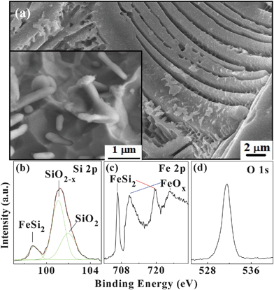 | ||
| Fig. 3 (a) SEM image of the etched β-FeSi2 powder without ultrasonic treatment. The bottom-left inset shows a local surface morphology. (b) Si 2 p, (c) Fe 2 p, and (d) O 1 s core level XPS spectra acquired from the β-FeSi2 nanowhisker powder. | ||
The etching mechanism of a silicon crystal is generally believed to be determined by the bond density and surface active energy.23,24 A unit cell in the crystal structure of β-FeSi2 has 48 atoms, including two elements, Fe and Si.25 Rebien et al.26 investigated the room-temperature oxide growth of β-FeSi2 after etching in NH4F and found that the oxidation kinetics of β-FeSi2 were very similar to that of silicon and there were no signs of iron oxide or segregated Fe or Si. The main product of oxidized β-FeSi2 is SiOx (x ≤ 2). In other words, the oxidization probability of silicon is much higher than that of iron in β-FeSi2 and it can be inferred that in hydrofluoric acid, the silicon in the β-FeSi2 can be dissolved more easily than iron. The X-ray photoelectron spectroscopy (XPS) spectra of the etched surface are presented in Figs. 3(b)–3(d). The Si 2 p and O 1 s spectra show strong SiO2−x (x < 2) peaks, whereas the Fe 2 p spectrum exhibits large FeSi2 and some FeOx peaks. The ratio of iron to silicon on the surface is calculated to be about 1:1, indicating that more silicon is oxidized and removed by the solution. This is consistent with our conclusion.
Fig. 4 depicts a schematic illustration of the anisotropic etching process of the microscale β-FeSi2 grain. We consider a β-FeSi2 crystal in HF [Fig. 4(a)]. Si and Fe on the crystal surface are continuously dissolved by HF, but owing to the different etching rates of Si and Fe, the facets with more Fe atoms (higher Fe ion density) have lower etching rates, whereas those with more Si atoms have higher etching rates. Some facets perpendicular to the <400> direction are all Fe atoms (grey balls) and have the highest Fe ion densities. Hence, the etching rate of the <400> direction is the lowest and the nanowhisker mainly grows along the <400> direction. However, the (022) facet parallel to the <400> direction is an all-Si atom plane [yellow balls in Fig. 4(b)]. The etching rate of the (022) plane is much higher than those of the Fe atomic planes and thus β-FeSi2 crystal is more easily dissolved along the (022) plane, forming deep rectangular grooves as shown in Figs. 3(a) and 4(b). In a corrosive environment, some sharp components are more easily etched. Therefore, with further etching, these regions are gradually smoothed and finally the cuboid NCs with abrupt walls transform into nanoneedles [Fig. 4(c)]. With increasing etching time, the interaction with the substrate becomes weaker and finally, β-FeSi2 nanowhiskers are formed by ultrasonic vibration.
 | ||
| Fig. 4 (a)–(c) Schematic illustration of the formation process of the β-FeSi2 nanowhisker. Grey and yellow balls stand for Fe and silicon atoms, respectively. | ||
This work was supported by National Basic Research Programs of China under Grant No. 2011CB922102 and PAPD. Partial support was also provided by National Natural Science Foundation (No. 60976063).
References
- D. Leong, M. Harry, K. J. Reeson and K. P. Homewood, Nature, 1997, 387, 686 CrossRef CAS.
- M. C. Bost and J. E. Mahan, J. Appl. Phys., 1985, 58, 2696 CrossRef CAS.
- G. K. Dalapati, S. L. Liew, A. S. W. Wong, Y. Chai, S. Y. Chiam and D. Z. Chi, Appl. Phys. Lett., 2011, 98, 013507 Search PubMed.
- T. Kim and J. P. Bird, Appl. Phys. Lett., 2010, 97, 263111 Search PubMed.
- N. Dahal and V. Chikan, Chem. Mater., 2010, 22, 2892 CrossRef CAS.
- C. M. Sun, H. K. Tsang, S. P. Wong, W. Y. Cheung, N. Ke and S. K. Hark, Appl. Phys. Lett., 2008, 92, 211902 Search PubMed.
- T. Yamada and H. Yamane, Chem. Mater., 2007, 19, 6047 Search PubMed.
- Y. J. Nakama, K. Minakawa, J. Ohta and M. Nunoshita, Appl. Phys. Lett., 2007, 91, 203102 Search PubMed.
- S. W. Hung, P. H. Yeh, L. W. Chu, C. D. Chen, L. J. Chou, Y. J. Wu and L. J. Chen, J. Mater. Chem., 2011, 21, 5704 RSC.
- H. T. Chen, X. L. Wu, Y. Y. Zhang and W. N. Su, Appl. Phys. A: Mater. Sci. Process., 2009, 97, 725 Search PubMed.
- Y. Nakamura, Y. Nagadomi, S. P. Cho, N. Tanaka and M. Ichikawa, Phys. Rev. B: Condens. Matter Mater. Phys., 2005, 72, 075404 Search PubMed.
- N. Yasui, R. Horie, Y. Ohashi, K. Tanji and T. Den, Adv. Mater., 2007, 19, 2797 Search PubMed.
- Q. Wan, T. H. Wang and C. L. Lin, Appl. Phys. Lett., 2003, 82, 3224 Search PubMed.
- H. F. Liu, A. Huang and D. Z. Chi, J. Appl. Phys., 2011, 109, 083538 Search PubMed.
- G. Z. Cambaz, G. N. Yushin, Y. Gogotsi and V. G. Lutsenko, Nano Lett., 2006, 6, 548 Search PubMed.
- J. Zhu, Z. Liu, X. L. Wu, L. L. Xu, W. C. Zhang and P. K. Chu, Nanotechnology, 2007, 18, 365603 CrossRef.
- L. Martinelli, E. Grilli, D. B. Migas, L. Miglio, F. Marabelli, C. Soci, M. Geddo, M. G. Grimaldi and C. Spinella, Phys. Rev. B: Condens. Matter, 2002, 66, 08532 Search PubMed.
- T. Qiu, X. L.Wu, F. Kong, H. B. Ma and P. K.Chu, Phys. Lett. A, 2005, 334, 447 Search PubMed.
- H. Kakemoto, Y. Makita, Y. Kino, S. Sakuragi and T. Tsukamoto, Thin Solid Films, 2001, 381, 251 Search PubMed.
- A. G. Birdwell, R. Glosser, D. N. Leong and K. P. Homewood, J. Appl. Phys., 2001, 89, 965 Search PubMed.
- D. H. Feng, Z. Z. Xu, T. Q. Jia, X. X. Li and S. Q. Gong, Phys. Rev. B: Condens. Matter, 2003, 68, 035334 Search PubMed.
- X. L. Wu, J. Y. Fan, T. Qiu, G. G. Siu and K. Chu Paul, Phys. Rev. Lett., 2005, 94, 026102 CrossRef CAS.
- H. A. Waggener, J. Syst. Technol., 1970, 3, 473 Search PubMed.
- H. Seidel, L. Csepregi, A. Heuberger and H. Baumgartel, J. Electrochem. Soc., 1990, 137, 3612 CAS.
- J. Tani and H. Kido, J. Alloys Compd., 2003, 352, 153 Search PubMed.
- M. Rebien, W. Henrion, H. Angermann and A. Roseler, Surf. Sci., 2000, 462, 143 Search PubMed.
| This journal is © The Royal Society of Chemistry 2012 |