Nanogravimetric study of lead underpotential deposition on selenium thin films as a semiconductor alloy formation procedure†
M. F.
Cabral‡
*,
M. L.
Calegaro
and
S. A. S.
Machado
Chemistry Institute of Sao Carlos, University of Sao Paulo, P.O. Box 780, 13560-970 Sao Carlos, SP, Brazil. E-mail: cabralmf@iqsc.usp.br
First published on 7th February 2012
Abstract
An electrochemical quartz crystal microbalanceAu electrode modified with a Se thin film was used to investigate the electrochemical behavior of lead ad-atoms using underpotential deposition (UPD) conditions. A specific quasi-reversible process was observed during the reduction of Pb2+ on Se thin films in perchloric acid media. The charge density of Pb ad-atoms on Se thin film (46.86 μC cm−2) suggests a recovery of 0.1 monolayers, which is in good agreement with EQCM data. The Se thin film can be successfully alloyed with Pb atoms that are deposited by chronoamperometry using time intervals large enough to allow for diffusion toward the inner Se phase. Linear sweep voltammetry combined with EQCM in perchloric acid was used to characterize the amount of Pb absorbed in the Se thin film. These findings offer a new strategy for alloy formation in semiconductor films using UPD as an effective tool to quantify the exact amount of the incorporated metal.
Introduction
Lead selenide, PbSe, is a small band-gap semiconductor (0.32 eV at 300 K) with a rocksalt crystal structure (i.e., face-centered cubic, FCC). It is widely used in infrared detectors, photographic plates, photographic absorbers, and lasers.1 It can be synthesized using a variety of procedures, including photochemical preparation,2 sonochemical synthesis,3 electrochemical atomic epitaxy,4pulsed laser deposition,5,6chemical bath deposition7 and electrochemical deposition.8,9The first report on electrochemical deposition of PbSe appeared in 1995,10 and the semiconductor film was obtained using a mixed electrolyte containing Pb(CH3COO)2 and H2SeO3, together with complexing agents, such as EDTA. The concentration ratio of Se to Pb was varied between 0.2 and 2. This pioneering work led to the publication of many subsequent reports that described an extensive variety of electrochemical techniques to obtain PbSe films. Among them, the work of Streltsov et al.11–15 can be considered to be the most extensively employed UPD technique. In these reports, the authors used electrolytes containing both Pb2+ and Se4+ ions in solution, with the electrode polarized at the proper potential program to obtain the PbSe film.
In general, the electrodeposition mechanisms for PbSe proposed by Streltsov are strongly dependent on the polarization potential and may proceed through any of the sequence of steps listed below:12
| SeO2 + 6H+ + 6e− → H2Se + 2H2O | (1) |
| Pb2+ + H2Se → PbSe + 2H+ | (2) |
Such a pathway requires that the polarization potential is sufficiently negative to generate H2Se on the electrode surface (approximately −0.6 V vs.Ag/AgCl12) to generate PbSe. If the electrode is kept in a more positive potential window, another possibility is the following:
| SeO2 + 4H+ + 4e− → Se0 + 2H2O | (3) |
| Pb2+ + 2e− → Pb0 | (4) |
| Pb0 + Se0 → PbSe | (5) |
The Nernst potentials for reactions (3) and (4) are +0.42 V and −0.39 V, respectively.12 Consequently, over a large potential window, Se can be deposited at an overpotential, whereas Pb electrodeposition occurs in the UPD range. Following Streltsov et al.,15 the simultaneous deposition of the Pb layer avoids passivation of the Se surface given the p-type semiconducting character of the amorphous film.
Recently, Xiao and co-workers published an extensive review partially covering the electrodeposition of PbSe.16 In this publication, it can be noted that such PbSe electrogeneration has been achieved, almost exclusively, from electrolytes containing both Pb2+ and Se4+, but the scope has been quite limited, and much more research is required to fully understand the mechanisms of Se combined with Pb, as well as the ad-atoms effect on the optical properties of such semiconductor films.
The objective of this paper is to study the underpotential deposition of Pb on a Se thin film as a tool to promote the blend of the semiconductive layer with Pb ad-atoms. This process will be accomplished with simultaneous nanogravimetric and voltammetric experiments in an electrolyte containing only Pb2+ ions. In particular, the objectives are to quantitatively analyze the mass/charge relationship (m/z) to provide information about the re-oxidation of ad-atoms on the modified surface and quantify the amount of Pb absorbed into the Se film.
Experimental section
Reagents
The electrolyte solutions were prepared with PA-grade Pb(ClO4)2 (Acrós) or SeO2 (Merck), Suprapur HClO4 (Merck) and water purified in a Millipore (Mille-Q) system. High purity N2 gas (White Martins) was first purged through the electrochemical cell, and the experiments were then performed at room temperature (25 °C).Apparatus
The working electrode (Au-EQCM) was a 5 MHz AT-cut quartz crystal disc with a diameter of 12.5 mm§. Both sides of the quartz crystal were covered with thin gold films (1.37 cm2 and 0.21 cm2) deposited over a Ti adhesion layer, but only one of the faces (1.37 cm2) was exposed to the electrolyte. The reference electrode used in this study was Ag/AgCl (saturated in 3 mol L−1KCl), and the auxiliary electrode was Pt foil with a geometric area of 1 cm2.The electrochemical instrumentation consisted of an Autolab potentiostat (PGSTAT30, Ecochimie, The Netherlands) linked to a PC-AMD K6-II microcomputer and a quartz crystalmicrobalance (RQCM Maxtek Inc®). The appropriate software was employed from AUTOLAB and Maxtek Inc®, respectively.
Electrogeneration of Se thin films and characterization
The Se thin films were deposited onto Au-EQCM by potentiostatic polarization at +0.10 V for 600 s in 1.0 M HClO4 with 1 mM SeO2 (Eeq = +0.70 V; t = 2 s), without magnetic stirring.17 After modification of the Au-EQCM with the Se thin film (before each UPD experiment), it was considered that the Se modification was a rigid film; therefore, the mass changes were taken to be proportional to the changes in the resonant frequency of the quartz crystal and were calculated according to the Sauerbrey equation.18To normalize the current and mass values obtained through the present work the roughness mean square (RMS) data obtained from AFM measurements were used as a normalization factor. The RMS data can bring information about the surface roughness of the Se thin film and in this present work it was equal to 13.95 (dimensionless) calculated from the Se thin film prepared after 600 s of polarization. The parameters evaluated to obtain the RMS values are described in Ref. 19. Finally, to characterize the Se thin film and PbSe alloy by X ray diffractometry (XRD) analysis, samples were prepared using a conductive glass (tin-doped indium oxide (ITO)). AFM measurements were well explained in Ref. 17. XRD analysis were performed using a Rigaku diffractometer (model RU200B) with Cu-Kα radiation (1.54 Å, 50 kV and 100 mA).
Results and discussion
Voltammetric and EQCM experiments.
The voltammetric profiles of the species being analyzed were collected and are shown in Fig. 1. Prior to understanding the voltammetric behavior of lead ad-atoms on selenium thin films, important features of this film were clarified as follows. We prepared the film in an electrolyte containing 1.0 mol L−1HClO4 with 1 × 10⁻³ mol L−1SeO2 by polarizing the electrode at 0.1 V (vs.Ag/AgCl) for 600 s and its thickness was estimated, based on EQCM measurements, as approximately 2 nm (8 monolayers of selenium atoms).17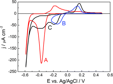 | ||
| Fig. 1 First cyclic voltamograms for an Au-EQCM electrode modified with a Se thin film under several conditions: (a) in 1.0 mol L−1HClO4, in a potential window defined by Einitial = 0.5 V, Einversion = −0.6 V and Efinal = 0.5 V (red line); (b) in 1.0 mol L−1HClO4 with 1 × 10⁻³ mol L−1Pb (ClO4)2, in a potential window between 0.5 and −0.25 V (blue line); (c) in 1.0 mol L−1HClO4 with 1 × 10⁻³ mol L−1Pb (ClO4)2, between 0.5 and −0.6 V (black line). Scan rate = 0.1 V s−1. | ||
To understand the recovery from Pb ad-atoms, we considered the surface atoms’ density. For this, the Se thin film was structurally characterized by XRD analysis (see ESI†, Fig. S1). As evidenced, some crystallographic peaks were indexed and a contribution from different crystallographic planes can be observed. So, taking into account that the thin film has a hexagonal closest-packed (hcp) unit cell, the surface density of Se atoms can be calculated as equal to 2.19 × 10¹⁵ atoms of Se per cm2 (Fig. S2†). In this way, such a value will be considered to evaluate the lead underpotential deposition.
The voltammogram shown as line A (red line) of Fig. 1 is obtained using an electrode surface modified by the thin Se film obtained under the conditions reported and analyzed above. The potential of this modified electrode was scanned between 0.5 and −0.6 V, in 1.0 mol L−1HClO4 at 0.1 V s−1. Here, the only electrode process observed is the Se reduction at −0.4 V, as discussed above. In the reverse scan, an anodic peak is observed at −0.2 V and is likely associated with the oxidation of H2Se. The second curve displayed as line B (blue line) in Fig. 1 represents the electrochemical process of Pb UPD on the Se thin film surface. This UPD process was performed in 1.0 mol L−1Pb(ClO4)2 with 1.0 mol L−1HClO4. Here, the electrode potential was swept between 0.50 V and −0.25 V at 0.1 V s−1. It is important to notice that, in such a potential window, line B shows no electrochemical processes related to Se occurring on the electrode surface. Hence, the cathodic peak observed at −0.15 V can be associated with a Pb UPD process and the anodic peak at 0.15 V, with the redissolution of Pbads. This surface process will be further discussed in subsequent paragraphs. Pb overpotential deposition (OPD) is not observed in line B of Fig. 1 because the Nernst potential for the Pb(II)/Pb couple is −0.39 V, as discussed previously. Finally, line C (black line) shows the voltammetric behavior of the Se thin film in 1.0 mol L−1Pb(ClO4)2 with 1.0 mol L−1HClO4, at 0.1 V s−1. The potential scan is extended over the region where Se is reduced to H2Se, but the cathodic peak related to this process, at −0.4 V, is weak in the voltammogram. This inhibition of H2Se formation is associated with the presence of a Pb monolayer that stabilizes the Se surface, thus preventing its reduction. This is our first direct evidence of Pb UPD and shows the stability of the obtained metal monolayer because the electrode was moved from the solution containing lead ions to the acid solution without losing the ad-atoms.
A charge density of 46.86 μC cm−2 for Pbadsoxidation (for the first cycle—line B) was obtained from the voltammetric profile by integration of the area under the curve between −0.04 V and 0.25 V. To interpret this charge density value, a discussion concerning the surface density of Se atoms is required. As mentioned above, 2.18 × 10¹⁵ atoms of Se per cm2 can be considered in a hcp unit cell and taking into account the transference of one electron per Se atom, a value equal to 350 μC cm−2 (atoms per cm2 × electron charge) can be expected. In this way, the experimental value of 46.86 μC cm−2 that is obtained for Pb UPD (two electron transference) yields a recovery equal to 0.1 monolayer, which indicates that each Pb ad-atom also occupies two Se atoms on the surface.
To further expand the analysis of the Pb UPD process, the mass variation profile for a Se thin film in an electrolyte containing Pb2+, under the same experimental conditions described for line B in Fig. 1, is presented in Fig. 2, together with the first cyclic voltammogram obtained simultaneously with the gravimetric experiment. Here, the massogram (dotted line) indicates that Pb UPD is a reversible process with the electrode mass returning to its original value after the entire cycle. Similar results have already been reported20,21 for Pb UPD on Au electrodes. Taking into account the oxidation sweep of Pb ad-atoms, between −0.4 V and 0.5 V, the mass variation was around 55 ng cm−2. The theoretical value for mass variation can be found using the relationship between the molar mass of Pb (MPb), and the surface density of Se atoms per cm2 and the number of moles of Se per cm2 according to eqn (6) and knowing that in 2.18 × 10¹⁵ atoms of Se per cm2 one has 3.62 × 10⁻⁹ mol of Se atoms per cm2 using Avogadro’s law:
| Δmtheoretical = MPb × 3.62 × 10⁻⁹ mol of Se atoms per cm2 | (6) |
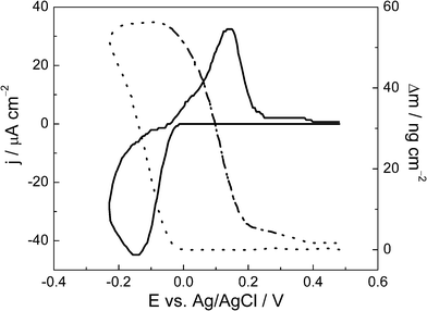 | ||
| Fig. 2 First cyclic voltammogram (full line) and mass variation profile (dotted line) for Pb UPD on a Se thin film in 1.0 mol L−1HClO4 with 1 × 10⁻³ mol L−1Pb(ClO4)2 at 0.10 V s−1. | ||
As the atomic mass of Pb is 207.2 g mol−1, the theoretical mass for the total occupancy of the Se atoms on the thin film surface is 745 ng cm−2. However, the voltammetric charge showed a recovery equal to 0.1 mL, therefore we may expect a theoretical mass variation equal to 74 ng cm−2. The experimental value of mass variation obtained from Fig. 2 is 55 ng cm−2, in a reasonable agreement with the voltammetric data. Following with the interpretation of the mass variation data, Fig. 3 shows the Δm vs. Δq plot for Pb UPD, where Δm is obtained from the massogram, while Δq came from the respective voltammogram, in the same potential region. Following Faraday's Law, the slope of the straight line obtained is associated with M/nF:
 | (7) |
 | (8) |
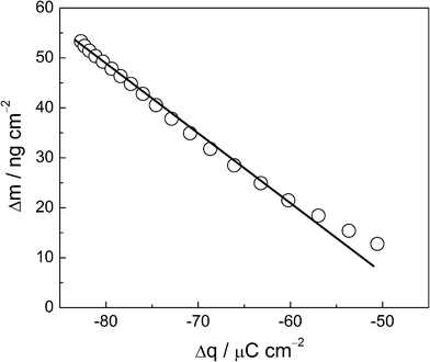 | ||
| Fig. 3 Δm vs. Δq plots for Pb UPD oxidation, under the same experimental conditions as given in Fig. 2. | ||
In this way, the slope of each linear segment of the plot is related to the molar mass of the electroactive species.22,23 An analysis of Fig. 3 shows a line between −0.04 V and 0.2 V that can be approximated by a linear fitting procedure. The slope of this section is calculated to be 1.12 × 10⁻³ g C−1, a value very close to the theoretical value for the atomic mass of Pb, divided by nF (1.07 × 10⁻³ g C−1), assuming the transfer of two electrons per lead atom. This indicates an electrochemical process involving Pbads → Pb2+ + 2e− from the Se thin film.
Chronoamperometric, linear voltammetry-nanogravimetric experiments and XRD analysis.
The degree of selenium alloyed with Pb was obtained using a chronoamperometric experiment. In Fig. 4, the chronoamperogram (a) and the mass variation (b) can be observed for the Se thin film in a solution containing 1.0 mM Pb(ClO4)2 with 1.0 M HClO4. The UPD potential of −0.2 V was chosen as it corresponds to the potential for Pb UPD but is more positive than that for the OPD. This polarization was applied to the selenium thin film surface for 600 s (the equilibrium potential and time were 0.5 V and 2 s, respectively).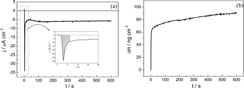 | ||
| Fig. 4 (a) Potentiostatic current transient and (b) gravimetric transient for the UPD Pb on a Se thin film in 1.0 mol L−1HClO4 with 1 × 10⁻³ mol L−1Pb(ClO4)2 at −0.20 V. | ||
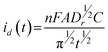
The chronoamperogram presented in Fig. 4a indicates that Pb UPD reaches a limiting diffusion current that stabilizes after approximately 100 s, at −6.0 μA cm−2. The insert in Fig. 4a shows, in the hatched area, the part of the transient that can be associated to the first stage during the Pb UPD process on the Se thin film. In these conditions for the Pb UPD process, after approximately 7 s the chronoamperometric response is rather unexpected for UPD processes because after the full surface coverage is reached, the electrochemical process should cease due to the positive overpotential value, which is insufficient to promote an overpotential deposition process. In this way, at the concentration range analyzed in the present work, the UPD process is not controlled by ionic diffusion from the solution towards the electrode surface. To understand such a process, one has to assume that the Pb ad-atoms diffuse to the inner layer of the Se thin film, described as solid phase diffusion, liberating more unbound surface atoms of Se to continue the UPD process. If, in a preliminary approach, the diffusion current is included in the Cottrell equation:
 | (9) |
The mass variation observed in the same chronoamperometric experiment was approximately 90 ng cm−2 (Fig. 4b). Thus, more than 1.5 layers of Pb were deposited in the selenium phase because one layer corresponds to the experimental mass variation of 55 ng cm−2, as discussed above.
Fig. 5 shows the diffraction patterns of the as-prepared Se thin film and PbSe alloy deposited onto a conductive glass substrate. The Joint Committee on Powder Diffraction Standards (JCPDS) database was used to evaluate the XRD response. It was evident after this procedure that the diffraction peaks of the semiconductor film are a combined response of Se and PbSe alloy phase. A single peak centered at around 30° was assigned to the glass substrate. To confirm the structural features discussed above, the Checkcell software25 was used to analyze the XRD response in order to evaluate the space group as well as the network parameter of the film components. The results presented in Table 1 show that there is a good agreement between the experimental and reference data confirming that PbSe has been successfully formed and that the diffraction peaks presented in Fig. 5 are composed of a mixed signal of Se and PbSe alloy.
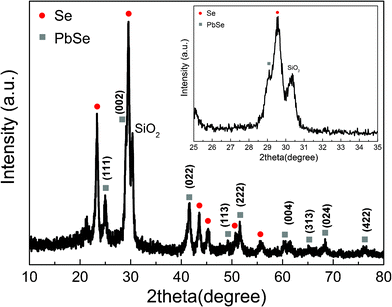 | ||
| Fig. 5 XRD patterns of PbSe alloy. The indexed peaks are marked by the filled circles (●) for Se (JCPDS pdf # 86-2246) and filled squares (■) for PbSe (JCPDS pdf # 77-245). For detailed peak positions and assignments, see Table 1. | ||
To confirm the alloy formation of the PbSe structure, after chronoamperometry, the quartz crystal and the electrochemical cell were washed thoroughly with ultrapure water, and the electrolyte solution was changed to 1.0 mol L−1HClO4. Linear stripping was performed together with the EQCM experiment, and both voltammetric and mass profiles for the Se thin film alloyed with Pb can be observed in Fig. 6, where the full line represents the voltammetric response at 0.1 V s−1 and the dotted line is associated with the massogram, collected simultaneously with the voltammogram. The voltammetric peak at 0.17 V can be assigned to Pb UPD re-oxidation. The mass and charge density variations, between −0.02 V and 0.60 V, was approximately 60 ng cm−2 and 40 μC cm−2, respectively, which are close to the values observed in the previously discussed chronoamperometric and nanogravimetric data for the Pb UPD process.
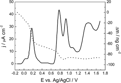 | ||
| Fig. 6 Linear sweep voltammogram for a Se thin film after the potentiostatic UPD Pb at −0.20 V (full line) and a mass variation profile (dotted line) in 0.1 mol L−1HClO4. Scan rate = 0.10 V s−1. | ||
The peaks at 0.77 V and 0.93 V might be associated with the oxidation of bulk selenium and Se UPD.26,27 The peaks at 1.10 V and 1.4 V can be associated with an intermetallic Au–Se compound.28,29 After 0.6 V, the small mass variation observed (about 20 ng cm−2) can be attributed to the adsorption of water and anions (perchlorate) on the Se thin film surface. It can be noted that the oxidation of the Se film (a four electron reaction), which generates Se(IV), does not show an associated mass loss as the Se4+ ions leave the electrode surface, as has been described previously.17
In the potential window explored in Fig. 6, no anodic peak could be attributed to the oxidation of potential PbSe species. This suggests that the Pb ad-atoms that are diffused throughout the Se thin film react with Se forming the PbSe alloy, as suggested by the XRD data. The respective mass variations associated with Pb dissolution (50 ng cm−2) showed some disagreement with the results obtained from the chronoamperograms, as shown in Fig. 4, which indicated a mass gain of 90 ng cm−2 for Pb UPD. This discrepancy suggests that some Pb still remains embedded within the Se thin film and that the oxidation of Pb and Se were incomplete in this potential sweep.
Conclusions
The combination of EQCM and CV techniques proved useful in the investigation of Pb UPD as a alloying methodology for Se thin film surfaces. The charge and mass variations associated with the Pb UPD showed that, after a prolonged polarization, more than a monolayer of Pb is deposited on the Se film, which is only possible if Pb ad-atoms can diffuse inside the Se phase, liberating more free surface atoms to continue the UPD process. This provides a very convenient methodology to alloy the Se film in an extremely controlled manner to alter the semiconducting properties of such layers. It was reinforced by XRD data showing the formation of PbSe structures. Studies on perturbing the band-gap by varying the amount of Pb are now possible at a level of precision that has never before been achieved. The same methodology can be applied to other semiconductor dopants, such as Zn and Cd, and can associate the alloyed amount with the semiconductor properties.Acknowledgements
We express our gratitude to Professor Guilherme M. Sipahi from the Physics Institute of São Carlos for fruitful discussions. The authors wish to thank Fundação de Amparo à Pesquisa do Estado de São Paulo (FAPESP–Proc. 04/09906-3) and Conselho Nacional de Desenvolvimento Científico e Tecnológico for financial support.References
- R. B. Kale, S. D. Sartale, V. Ganesan, C. D. Lokhande, Y.-F. Lin and S.-Y. Lu, Appl. Surf. Sci., 2006, 253, 930 CrossRef CAS.
- W.-B. Zhao, J.-J. Zhu and H.-Y. Chen, J. Cryst. Growth, 2003, 252, 587 CrossRef CAS.
- T. Ding, H. Wang, S. Xu and J.-J. Zhu, J. Cryst. Growth, 2002, 235, 517 CrossRef CAS.
- R. Vaidyanathan, J. L. Stickney and U. Happek, Electrochim. Acta, 2004, 49, 1321 CrossRef CAS.
- R. T. Rumianowski, R. S. Dygdala, W. Jung and W. Bala, J. Cryst. Growth, 2003, 252, 230 CrossRef CAS.
- M. Frumar, B. Frumarova, P. Nemec, T. Wagner, J. Jedelsky and M. Hrdlicka, J. Non-Cryst. Solids, 2006, 352, 544 CrossRef CAS.
- P. P. Hankare, S. D. Delekar, V. M. Bhuse, K. M. Garadkar, S. D. Sabane and L. V. Gavali, Mater. Chem. Phys., 2003, 82, 505 CrossRef CAS.
- L. Beaunier, H. Cachet and M. Froment, Mater. Sci. Semicond. Process., 2001, 4, 433 CrossRef CAS.
- Z. Zainal, A. J. Ali, A. Kassim and M. Z. Hussein, Sol. Energy Mater. Sol. Cells, 2003, 79, 125 CrossRef CAS.
- A. N. Molin and A. I. Dikusar, Thin Solid Films, 1995, 265, 3 CrossRef CAS.
- E. A. Streltsov, N. P. Osipovich, L. S. Ivashkevich and A. S. Lyakhov, Electrochim. Acta, 1999, 44, 2645 CrossRef CAS.
- E. A. Streltsov, N. P. Osipovich, L. S. Ivashkevich, A. S. Lyakhov and V. V. Sviridov, Electrochim. Acta, 1997, 43, 869 CrossRef.
- E. A. Streltsov, S. K. Poznyak and N. P. Osipovich, J. Electroanal. Chem., 2002, 518, 103 CrossRef CAS.
- A. S. Bondarenko, G. A. Ragoisha, N. P. Osipovich and E. A. Streltsov, Electrochem. Commun., 2005, 7, 631 CrossRef CAS.
- D. K. Ivanov, N. P. Osipovich, S. K. Poznyak and E. A. Streltsov, Surf. Sci., 2003, 532–535, 1092 CrossRef CAS.
- F. Xiao, C. Hangarter, B. Yoo, Y. Rheem, K.-H. Lee and N. V. Myung, Electrochim. Acta, 2008, 53, 8103 CrossRef CAS.
- M. F. Cabral, V. A. Pedrosa and S. A. S. Machado, Electrochim. Acta, 2010, 55, 1184 CrossRef CAS.
- K. Park, M. Koh, C. Yoon, H. W. Kim and H. D. Kim, J. Supercrit. Fluids, 2004, 29, 203 CrossRef CAS.
- V. Kelley, C. Kowalski and T. Geschwender, NanoScope Software 6.13 User Guide, Veeco Instruments Inc., 2004.
- M. R. Deakin and O. Melroy, J. Electroanal. Chem., 1988, 239, 321 CrossRef CAS.
- J. Lee, H. Varela, S. Uhm and Y. Tak, Electrochem. Commun., 2000, 2, 646 CrossRef CAS.
- N. Furuya and S. Motoo, J. Electroanal. Chem., 1979, 102, 155 CrossRef CAS.
- T. E. Lister and J. L. Stickney, J. Phys. Chem., 1996, 100, 19568 CrossRef CAS.
- M. P. Gomez, D. A. Stevenson and R. A. Huggins, J. Phys. Chem. Solids, 1971, 32, 335 CrossRef CAS.
- J. Laugier and B. Bochu, Checkcell—A Software Performing Automatic Cell/Space Group Determination, Collaborative Computational Project Number 14 (CCP14), Laboratoire des Matériaux et du Génie Physique de l'Ecole Supérieure de Physique de Grenoble (INPG), France, 2000.
- C. Wei, N. Myung and K. Rajeshwar, J. Electroanal. Chem., 1994, 375, 109 CrossRef CAS.
- M. F. Cabral, H. B. Suffredini, V. A. Pedrosa, S. T. Tanimoto and S. A. S. Machado, Appl. Surf. Sci., 2008, 254, 5612 CrossRef CAS.
- M. S. Kazacos and B. J. Miller, J. Electrochem. Soc., 1980, 127, 5 CrossRef.
- R. W. Andrews and D. C. Johnson, Anal. Chem., 1975, 47, 294 CrossRef CAS.
Footnotes |
| † Electronic supplementary information (ESI) available. See DOI: 10.1039/c2ra00847e |
| ‡ Present address: Department of Genetics, Evolution and Bioagents, Institute of Biology CP 6109, University of Campinas, 13083-970, Campinas, SP, Brazil. |
| § According to the INFICON brochure and datasheets, the quartz crystal plates recovered with gold films are unpolished. (http://www.inficonthinfilmdeposition.com/en/maxtekrqcm.html) |
| This journal is © The Royal Society of Chemistry 2012 |