Direct patterning of poly(3-hexylthiophene) and its application to organic field-effect transistor†
Yuta
Saito
a,
Yoshimasa
Sakai
b,
Tomoya
Higashihara
a and
Mitsuru
Ueda
*a
aDepartment of Organic and Polymeric Materials, Tokyo Institute of Technology, 2-12-1-H120 O-okayama, Meguro-ku, Tokyo, 152-8552, Japan. E-mail: ueda.m.ad@m.titech.ac.jp
bMitsubishi Chemical Group, Science and Technology Research Center, Inc., 1000 Kamoshida-cho, Aoba-ku, Yokohama, 227-8502, Japan
First published on 15th December 2011
Abstract
A direct photolithographic patterning method of regioregular poly(3-hexylthiophene) (rr-P3HT) as a semiconductive layer of organic field-effect transistors (OFETs) has been developed. The performance (0.092 cm2/Vs) of a bottom-contact type OFET using the patterned rr-P3HT as a semiconductive layer was almost the same as that (0.10 cm2/Vs) using the pristine rr-P3HT.
Solution-processed π-conjugated polymers (πCPs) have emerged in an attractive class of materials accessible for optoelectronic applications due to their good processability for low-cost and large-areas. Among them, poly(3-hexylthiophene) (P3HT) and related thiophene-based polymers are of significant interest because of their facile synthesis, high charge mobility, and high processability. The high mobility of P3HT is primarily attributed to the formation of preferentially in-plane oriented π–π stacking leading to efficient in-plane charge transport.1 Based on these benefits, P3HT has been used in a wide variety of electronic devices, such as organic field-effect transistors (OFETs),2 organic photovoltaic cells,3 and sensors.4
A wide variety of techniques has been developed to pattern polymers such as direct writing by scanning probe microscopy, ink-jet printing, nano-imprinting, micro-contact printing, dry-etch processing by laser ablation, and photolithography.5 Generally, a micro-patterned P3HT film is fabricated by the micro-contact printing method with a poly(dimethylsiloxane) stamp.6 However, this method requires a complicated operation resulting in a low productivity. To overcome this problem, direct patterning onto polythiophenes based on a photolithographic method is highly required. Direct patterning onto a P3HT film was demonstrated when an exposed area became insoluble due to cross-linking of an alkyl chain by irradiation with UV light.7 However, the cross-linking of P3HT by irradiation required a huge exposure dose. To improve the sensitivity, Yeet al. reported a novel cross-linkable conjugated polythiophene with oxetane moieties attached to the polymer backbone via an alkyl spacer8 which was UV photopatterned in the presence of a photoinitiator. Although the polymer worked as a sensitive negative photoresist, the synthesis of the monomer still required several steps. Recently, Chang et al. reported efficient patterning methods of poly(2,5-bis(3-alkylthiophen-2-yl)thieno[3,2-b] thiophene) (PBTTT).9 The method involves multi-stage patterning transfer processes viadelamination using a poly(methyl methacrylate) dielectric film as a sacrificial layer. Quite recently, Qui et al. reported photopatternable semiconducting/insulating polymer blends.10 Although this blend system would have several advantages such as low material costs, improved environmental stability and mechanical properties, the OFET properties were not sufficient for practical applications. Therefore, the development of a simpler and more direct patterning system with maintaining high OFET properties is strongly demanded.
In a previous study, we briefly reported the direct patterning method of a P3HT film by photolithography.11 The head-to-tail (H-T) regioregularity of P3HT used as a matrix polymer is only 85%, and has a tendency to lead to an inadequate conjugation length, low crystallinity, and reduced chain packing. Indeed, regiorandom P3HT showed a several orders of magnitude lower electroconductivity than that of the regioregular P3HT (rr-P3HT).1 Taking into consideration that the H-T regioregularity strongly affects the electroconductivity and charge mobility, a regioregularity higher than 85% is necessary to further improve transistor device performance. Recently, two groups, McCullough et al. and Yokozawa et al., independently developed a simple method for the synthesis of rr-P3HTs with a narrow molecular distribution based on the quasi-living Grignard metathesis (GRIM) polymerization.12,13
In this paper, we report a direct patterning method of rr-P3HT based on photolithography using 4,4′-methylenebis(2,6-bis(methoxymethyl)phenol) (MBMP) as a cross-linker and diphenyliodonium-9,10-dimethoxyanthracene-2-sulfonate (DIAS) as a photoacid generator (PAG). The patterning process is depicted in Fig. 1. A photosensitive P3HT was prepared from a mixture of each component. In the exposed area, benzyl cations formed from MBMP can react with not only thiophene rings, but also the aromatic rings or hydroxy groups of MBMP, producing cross-linked polymers.14 The reactivity of the hydroxy groups is higher than that of the aromatic rings and thiophene rings. The rr-P3HT film has a strong absorption in the UV and visible regions, but also has a window at 300 nm. DIAS could be decomposed by UV exposure because of its strong absorption at 350–450 nm (see Supporting Information†), so the combination of P3HT and DIAS was suitable for this system. As a further demonstration, we also report the fabrication and characterization of an OFET device embedding the micropatterned P3HT as a semiconducting layer.
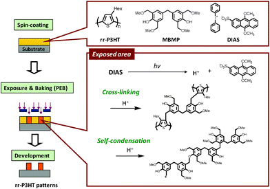 | ||
| Fig. 1 Photolithographic mechanism for patterning of rr-P3HT. | ||
rr-P3HT, used as the matrix polymer, was synthesized by the GRIM polymerization.12,13 The average molecular weight and polydispersity index of rr-P3HT were determined to be 12![[thin space (1/6-em)]](https://www.rsc.org/images/entities/char_2009.gif) 000 and 1.18, respectively, by gel permeation chromatography with a polystyrene standard. The regioregularity was calculated to be greater than 95% by the integral ratio of the 2.81 and 2.56 ppm peaks assignable to the methylene protons next to the thiophene rings in the 1H NMR spectrum.15
000 and 1.18, respectively, by gel permeation chromatography with a polystyrene standard. The regioregularity was calculated to be greater than 95% by the integral ratio of the 2.81 and 2.56 ppm peaks assignable to the methylene protons next to the thiophene rings in the 1H NMR spectrum.15
The 130–150 nm thick rr-P3HT films were obtained by spin-coating the solution of rr-P3HT, MBMP and DIAS on a silicon wafer, followed by prebaking at 80 °C for 1 min in air. To investigate the dissolution behavior of the exposed and unexposed areas of the films, the effect of the post-exposure bake (PEB) condition on the dissolution rate was studied. The PEB process to cause the cross-linking reactions is quite important for a chemical amplified photolithographic system. After exposure, these films were heated using the PEB process at a set of temperatures for a prescribed period of time, then developed with chloroform at room temperature. The effect of the PEB temperatures is shown in Fig. 2a. The dissolution rate in the exposed area decreases with the increasing PEB temperature. On the other hand, the dissolution rate in the unexposed area is unchanged. A very high dissolution contrast is obtained at the PEB conditions between 140 and 170 °C for 1 min. This result indicates that the cross-linking reaction is effectively promoted under the PEB conditions. The loading ratios of MBMP and DIAS on the dissolution rate of the polymer films were optimized for control of the dissolution rate. It is expected that MBMP and DIAS may inhibit carrier transportation in the semiconductive layer of the OFETs, so the MBMP and DIAS loading should be minimized. The dissolution rates of the exposed and unexposed areas with several MBMP and DIAS loading are shown in Fig. 2b–2c. The dissolution rate in the exposed area decreased with the increasing DIAS loading and the P3HT film became insoluble in chloroform with more than 5 wt% DIAS. The effect of the MBMP loading on the dissolution rate is similar to that of the DIAS loading. More than 5 wt% MBMP results in an insoluble P3HT film at the exposed area.
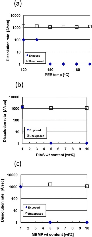 | ||
| Fig. 2 Effect of (a) PEB temperature, (b) DIAS loading content, and (c) MBMP loading content on dissolution rate for the rr-P3HT film in the exposed and unexposed areas. Film compositions of rr-P3HT/MBMP/DIAS in (a) was fixed at 80/10/10 wt%. The MBMP weight content in (b) was fixed to 10 wt%. The DIAS weight content in (c) was fixed to 5 wt%. PEB conditions in (b) and (c) were fixed at 160 °C for 1 min and 170 °C for 1 min, respectively. Non-filter exposure time was fixed at 5 min and chloroform was used as the developer. | ||
Based on these preliminary optimization studies, an optical images of the contact-printed pattern was obtained using the resist system shown in Fig. 3. The resist film consisting of rr-P3HT (90 wt%), MBMP (5 wt%), and DIAS (5 wt%) was pre-baked at 120 °C for 1 min, exposed with UV light for 5 min, post-baked at 170 °C for 30 s, and developed with chloroform. Consequently, a clear negative pattern was easily obtained with 15 μm features on a 100 nm thick film.
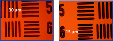 | ||
| Fig. 3 Optical image of patterned rr-P3HT films. The resist film consisting of rr-P3HT (90 wt%), MBMP (5 wt%), and DIAS (5 wt%) was exposed with UV light for 5 min, post-baked at 170 °C for 30 s, and developed with chloroform. | ||
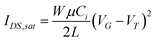
The solution of rr-P3HT, MBMP, and DIAS allowed us to study the fabrication of OFETs by a photolithographic pattering process. OFET devices incorporating MBMP and DIAS compounds as cross-linkable components with a bottom-contact configuration were fabricated on an n-doped Si/SiO2 substrate and gold-chromium bilayer source/drain electrodes by a simple spin-coating process from a 1,1,2,2-tetrachloroethane solution. The data for the OFET characteristics are summarized in Table 1. The mobility was calculated using the following equation:
 | (1) |
| Organic semiconductor | Mobility | Threshold voltage | on/off ratio |
|---|---|---|---|
| μ (cm2/Vs) | V T (V) | I ON/IOFF | |
| Patterned rr-P3HT | 0.026 | 7.5 | 2.5 × 10⁶ |
| Patterned rr-P3HT (dedoped) | 0.092 | −1.6 | 5.4 × 10⁶ |
| Pristine rr-P3HT | 0.10 | −0.69 | 5.9 × 10⁷ |
Although the OFET using the patterned rr-P3HT exhibits typical p-type characteristics after a thermal treatment at 180 °C for 30 min, the charge carrier mobility and threshold voltage are 0.026 cm2 V−1 s−1 and 7.5 V, respectively, which suggest some doping of rr-P3HT by the remaining PAG residue (Fig. 4a). To remedy this problem, additional thermal and dedoping treatments were carried out after development. The patterned film on SiO2 was first heated at 200 °C for 30 min to completely decompose the PAG, then treated with a 1 wt% aqueous ammonia solution for 30 min at room temperature, followed by thermal annealing at 180 °C for 30 min. The resulting device exhibited a high charge carrier mobility in the saturation region of 0.092 cm2 V−1 s−1, low threshold voltage of −1.6 V, and high on/off current ratio of 5.4 × 10⁶ in the 10 μm channel length (Fig. 4b). On the other hand, the charge carrier mobility, threshold voltage, and on/off ratio of a pristine rr-P3HT film were 0.10 cm2 V−1 s−1, −0.69 V, and 5.9 × 10⁷, respectively (Fig. 4c). The characteristics of the OFET with the patterned rr-P3HT are almost same as those of the pristine P3HT. These results are summarized in Table 1, and indicate that the performance of rr-P3HT OFET bottom-contact devices is only slightly degraded by the patterning process and is sufficient for practical use.
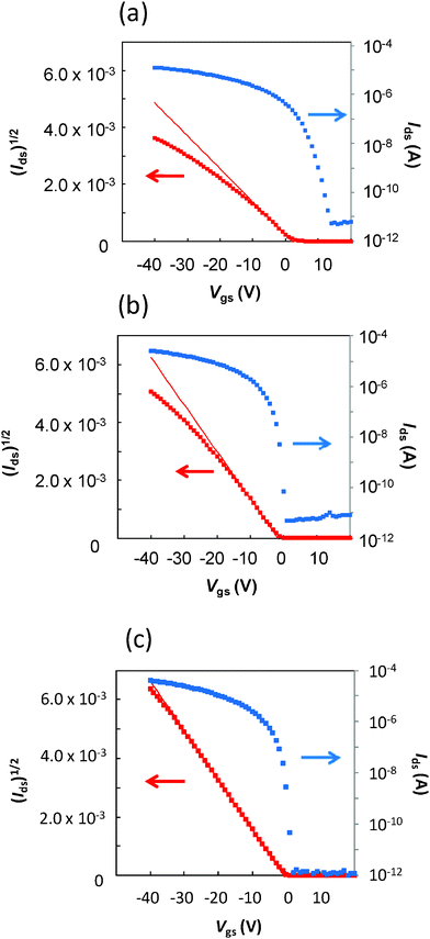 | ||
| Fig. 4 Plots of Ids and Ids1/2versus Vgs using the devices with patterned rr-P3HT (a), patterned and dedoped rr-P3HT (b), and pristine rr-P3HT (c) (L = 10 μm; W = 500 μm). | ||
In conclusion, we have developed a new and simple microfabrication method for a rr-P3HT film by photolithography. A clear negative pattern with 15 μm features was obtained using the rr-P3HT, MBMP, and DIAS system. In addition, the OFET performance using the patterned rr-P3HT as an organic semiconductor was almost the same as that using the pristine rr-P3HT. This result indicates that the developed system is useful and adapted to microfabrication of a wide variety of other conductive polymers because of its simple cross-linking mechanism.
References
- R. D. McCullough, Adv. Mater., 1998, 10, 93 CrossRef CAS.
- R. C. G. Naber, M. Mulder, B. De Boer, P. W. M. Blom and D. M. De Leeuw, Org. Electron., 2006, 7, 132 CrossRef CAS.
- S. Gunes, H. Neugebauer and N. S. Sariciftci, Chem. Rev., 2007, 107, 1324 CrossRef.
- M. Manceau, A. Rivaton and J. L. Gardette, Macromol. Rapid Commun., 2008, 29, 1823 CrossRef CAS.
- S. Holdcroft, Adv. Mater., 2001, 13, 1753 CrossRef CAS.
- S. K. Park, Y. H. Kim, J. I. Han, D. G. Moon, W. K. Kim and M. G. Kwak, Synth. Met., 2003, 139, 377 CrossRef CAS.
- M. S. A. Abdou, G. A. Diaz-Guijada, M. I. Arroyo and S. Holdcroft, Chem. Mater., 1991, 3, 1003 CrossRef CAS.
- K. Lu, Y. Guo, Y. Liu, C. Di, T. Li, Z. Wei, G. Yu, C. Du and S. Ye, Macromolecules, 2009, 42, 3222 CrossRef CAS.
- J. F. Chang and H. Sirringhaus, Adv. Mater., 2009, 21, 2530 CrossRef CAS.
- L. Qiu, Q. Xu, W. H. Lee, X. Wang, B. Kang, G. Lv and K. Cho, J. Mater. Chem., 2011, 21, 15637 RSC.
- K. Endo, T. Higashihara and M. Ueda, Polym. J., 2009, 41, 808 CrossRef CAS.
- M. C. Iovu, E. E. Sheina, R. R. Gil and R. D. McCullough, Macromolecules, 2005, 38, 8649 CrossRef CAS.
- R. Miyakoshi, A. Yokoyama and T. Yokozawa, J. Am. Chem. Soc., 2005, 127, 17542 CrossRef CAS.
- K. Mizoguchi and M. Ueda, J. Polym. Sci. Part A: Polym. Chem., 2008, 46, 4949 CrossRef CAS.
- S. Amou, O. Haba, K. Shirato, T. Hayakawa, M. Ueda, K. Takeuchi and M. Asai, J. Polym. Sci. Part A: Polym. Chem., 1999, 37, 1943 CrossRef CAS.
Footnote |
| † Electronic Supplementary Information (ESI) available: See DOI: 10.1039/c2ra00783e/ |
| This journal is © The Royal Society of Chemistry 2012 |