Low temperature growth of graphene film by microwave assisted surface wave plasma CVD for transparent electrode application
Golap
Kalita
*,
Koichi
Wakita
and
Masayoshi
Umeno
Department of Electronics and Information Engineering, Chubu University, 1200 Matsumoto-cho, Kasugai-shi, 487-8501, Japan. E-mail: golapkalita@yahoo.co.in; Tel: +81 568 51 1111; Fax: +81 568 51 1478
First published on 8th February 2012
Abstract
Here, we report the synthesis of a graphene film on Cu foil by microwave assisted surface wave plasma chemical vapor deposition (MW-SWP-CVD) at a low pressure and temperature using a hydrocarbon gas. Raman spectroscopy and transmission electron microscopy (TEM) studies clearly show deposited carbon films that consist of few layer graphene sheets. Deposition of graphene films with a few layers structure was achieved at a temperature as low as 240 °C. In the nucleation and growth process, carbon radicals are formed with hydrogen termination in the surface wave plasma, which absorb continuously on the Cu surface to form sp2 carbon and eventually a graphene structure. The transparency and conductivity characteristics of the transferred graphene films show suitability for flexible electronics applications.
1. Introduction
Graphene is a perfect two-dimensional (2D) carbon sheet and is the basic building block of graphite, fullerene, and carbon nanotubes. Graphene related materials have attracted much attention over the past few years, owing to their interesting electrical, mechanical, and chemical properties for electronic device applications.1–5 There have been lots of efforts to exploit the outstanding electrical and mechanical properties of graphene for the fabrication of transparent electrodes.6–10 In the present scenario, indium tin oxide (ITO) and related materials have been widely used as an electrode material in electronic devices as it possesses high conductivity and transmittance.11,12 The use of ITO, however, is becoming increasingly problematic due to the limited availability of indium (In) and intrinsic chemical and electrical drawbacks.13Graphene based materials can be a suitable alternative for ITO or other materials for transparent electrode applications. Synthesis of graphene can be achieved by different approaches, and among them, thermal CVD on a metal sheet and chemical reduction of graphene oxide appear to be the most suitable as transparent electrodes for electronic device applications.14–17 Recent progress in the CVD growth process makes it possible to synthesize continuous large area graphene, although the trends of thermal CVD synthesis involve a very high deposition temperature, typically around 1000 °C.9,18,19 A low temperature deposition technique can be more feasible for industrial applications and can pave the way for direct deposition on transparent flexible substrates. It has been observed that graphene film can be deposited from a solid precursor at low temperature; while no graphene formation from a gaseous source below 600 °C by a thermal CVD technique was obtanied.20 This might be due to insufficient energy for hydrogen detachment and graphene formation at low temperatures.
This shows the limitation of the thermal CVD process for low temperature growth of graphene film from different source gases. In this study, we present the deposition of a large area graphene film at a temperature as low as 240 °C by a MW-SWP-CVD technique. The technique has a special advantage as it can easily produce metre-scale uniform plasma, which can be suitable for the large area deposition of graphene films. Previously, we have developed and reported the same technique for the deposition of amorphous carbon films on Si substrate and different insulating substrates below 100 °C.21,22 The MW-SWP process can produce an over-dense plasma even at low gas pressures, with a density higher than the cut-off density (7.4 × 10¹⁶ m−3 for 2.45 GHz), without magnetic fields, and can be enlarged by employing a large dielectric window and multi-slot antenna. The MW-SWP process has very low electron temperatures and low plasma space potentials. Carbon radicals can form with hydrogen termination within the microwave plasma, which absorb continuously onto the Cu surface bonding with each other by a diffusion process to form sp2 carbon; as a result, graphene growth can be achieved at a much lower substrate temperature.
2. Experimental
Graphene films were deposited on Cu foil (25 μm) by using the MW-SWP-CVD technique. In the MW-SWP-CVD system a hollow quartz plate is taken as for plasma generation. It has been reported that, using a hollow plate, plasma can be started smoothly without any density jump and plasma density is two times higher than that for a flat plate. High density surface wave plasma can be generated in the metre-scale and large area deposition can be achieved at a very fast rate.23 The schematic representation of the system used for growth of the graphene film is shown in Fig. 1. For deposition of the graphene film a gas mixture of C2H2 (99.99 vol%) and Ar with a flow rate of 10 and 200 sccm (standard cubic centimetres per minute), respectively was used for all the experiments. Deposition was carried out on Cu foil without any pretreatment at a gas composition pressure of 45 Pa for a duration of 2–4 min. The microwave power used for deposition was 1.2 kW, having a negligible amount of fluctuation. Graphene films were deposited by varying the substrate temperature and deposition time. The synthesized large area graphene films were transferred to an arbitrary substrate by wet-etching the underlying Cu foil in a Fe(NO3)3 solution (concentration of 30 mg ml−1). Prior to the etching of the Cu foil, poly(methyl methacrylate) (PMMA) solution was dissolved in chlorobenzene at a concentration of 50 mg ml−1 and was drop cast and cured at 150 °C for 2 min. The PMMA–graphene stack was placed on the target substrate and a small amount of PMMA solution was drop cast to dissolve the pre-coated PMMA layer. The PMMA–graphene film on the target substrate was cured again at room temperature and then dissolved in acetone. Diluted HNO3 (10% concentration) treatment of the graphene films was carried out to remove the metal and other impurities.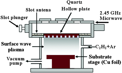 | ||
| Fig. 1 Schematic diagram of the microwave assisted surface wave plasma chemical vapor deposition system used for the low temperature deposition of graphene films. | ||
The graphene sheets were characterized with Raman spectroscopy having a laser excitation energy of 532 nm in a NRS 300 laser Raman spectrometer, X-ray photoelectron spectroscopy (XPS) in SSX-100, scanning electron microscopy (SEM) in FESEM, Hitachi S-4300 and high-resolution transmission electron microscope (HRTEM), JEOL:JEM-2100F operated at 200 kV. Optical transmittance characterization of the graphene sheets on glass were carried out with UV-Vis-NIR on a JASCO-V570 spectrophotometer. Sheet resistance measurements were carried out with a four probe technique.
3. Results and discussion
Graphene based films were deposited at a low temperature (<600 °C) and low pressure (45 Pa) using a gas mixture of C2H2 and Ar. Uniform deposition of graphene film on Cu foil with very good stability was obtained by the MW-SWP-CVD technique. Fig. 2(a) shows Raman studies at lower and higher wavenumbers of the carbon films deposited at 400 and 500 °C. As presented in the figure, a disorder-induced D band is observed at around 1348 cm−1, indicating phonon scattering at defect sites and impurities. An intense graphitic G band is also observed at around 1574 cm−1, attributing to the sp2 phonon vibrations. Three other peaks were observed at 2685, 2914, and 3210 cm−1 corresponding to 2D, G+D and 2G second-order Raman spectra, respectively. The second-order Raman spectrum of carbon materials is quite remarkable in order to study the structural quality and possible formation of graphene structure.24,25 The presence of an intense 2D and 2G peak indicates a good agreement of graphene structure formation in the carbon film. The Raman characteristic for the graphene film deposited at 400 and 500 °C is almost identical having a similar G and 2D peak intensity. The D peak and D+G peak in the graphene film shows the presence of defect sp2 sites. Similarly, Fig. 2(b) shows Raman studies at lower and higher wavenumbers of a carbon thin film deposited at 240, 270 and 300 °C. Defect induced D and graphitic G peaks were observed at around 1348 and 1581 cm−1, respectively. 2D, D+G and 2G Raman peaks at 2682, 2920 and 3212 cm−1, respectively, were also observed for the very low temperature deposited carbon film; corresponding to a few layers of graphene formation. The graphene films deposited at low temperatures, less than 300 °C, show enhancement of the D+G peak, presenting an increase in defect structure or graphene domain edges in the graphene film with a few layers. Recently, the presence of similar defect structures in a graphene film deposited by the surface wave assisted CVD process has been observed.26 While, at an elevated temperature a much higher quality graphene film can be synthesized using similar techniques.27,28 Again, the thermal CVD approach also shows much better quality graphene; though such a low temperature deposition is a challenge.9,18,29 The presence of clear 2D peak at a deposition temperature of 240 °C indicates graphene formation on the Cu foil. The formation of a few layers of graphene is possible at a low temperature as carbon radicals are formed by the plasma and do not have much effect on the substrate temperature. The generated carbon radical with hydrogen detachment within the microwave plasma can segregate on the Cu surface to form sp2 carbon. The Ar diluted C2H2 gas mixture shows the formation of a very stable plasma in a large area and thereby allows uniform carbon radical formation and deposition on the Cu foil. Again, the use of a hollow quartz plate for plasma generation shows a very smooth and high density surface wave plasma formation, which enables a rapid growth process with minimum ion bombardment on Cu foil. At present, the grown graphene films show the presence of defect structures. Further studies will be carried out by changing the gas composition; addition of a small amount of hydrogen can reduce the formation of disordered or defect structures by etching amorphous carbon.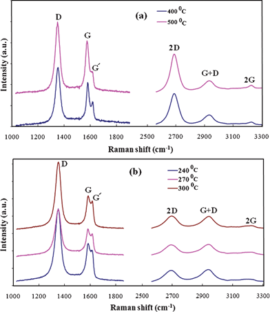 | ||
| Fig. 2 Raman spectra of a graphene film at (a) lower and (b) higher Raman shift, deposited at a substrate temperature of 400 and 500 °C. Raman spectra of a graphene film at (c) lower and (d) higher Raman shift, deposited at a substrate temperature of 240, 270 and 300 °C, indicating the presence of 2D peak and formation of a few layers of graphene. | ||
Fig. 3(a) shows the wide XPS spectra of the low temperature deposited graphene films on Cu foil. The wide XPS spectra clearly shows the presence of C1s and O1s peaks at around 284.5 and 532.4 eV, respectively without observing any other elements. Quantitative analysis indicates around 0.9 at% of oxygen for all the graphene films. The presence of oxygen may be due to surface chemi-absorption on the graphene surface and remains almost the same for all the graphene films. Fig. 3(b) shows the XPS spectra of the graphene films with photoelectron emission from the C1s core level peak centered at 284.5 eV corresponding to sp2 carbon. The C1s peak is similar to those for all the low temperature deposited carbon films without any change or shift of the peak position. The XPS study presents an almost identical sp2 carbon peak for 240 or 500 °C deposited graphene films.
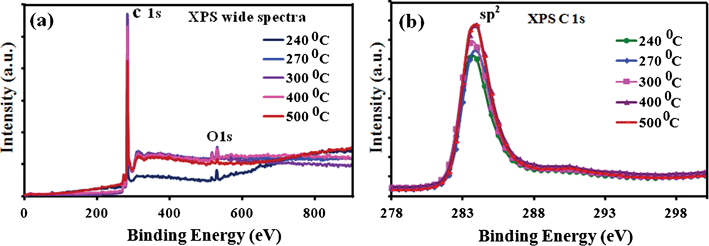 | ||
| Fig. 3 XPS studies of as deposited graphene film on Cu foil. (a) A wide XPS spectra and (b) C1s XPS spectra at different substrate temperatures is presented. | ||
Fig. 4(a) shows a SEM image of uniform graphene film formation on a Cu substrate deposited at 240 °C. The image shows the presence of Cu surface steps and grains having non-uniform graphene flakes. The graphene film has grain boundaries without formation of any nanostructured particles indicating that the graphene film is continuous and uniform under the plasma CVD deposition conditions. During the nucleation and growth process, carbon radicals in the plasma absorb continuously onto the Cu surface and bind with each other by a diffusion process to form sp2 carbon and eventually a continuous graphene film. Fig. 4(b) shows a SEM image of a graphene film transferred on to a plastic substrate for fabrication of a transparent electrode presenting wrinkle formation. The transferred graphene film on the plastic substrate is continuous and optically uniform; which can be suitable for transparent electrode applications.
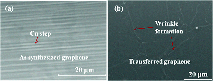 | ||
| Fig. 4 SEM images of graphene film on Cu deposited at 240 °C. (a) As grown graphene film on Cu foil presenting graphene grain and Cu steps. (b) A transferred graphene film on a plastic substrate presenting wrinkle formation. | ||
The structural morphology of the graphene film deposited at 240 °C was also characterized by HRTEM studies. Fig. 5(a) shows a TEM image of a graphene sheet, the edge and top of the graphene sheet as denoted by the red dotted box were investigated by HRTEM studies. The formation of a few layers of graphene can be observed at the folded edge rather than a monolayer, even though there are defects in the graphene layers. The results of the HRTEM study of the folded edge of graphene correlates with the Raman study of the formation of a few layers of graphene. Fig. 5(b) shows a graphene sheet with a few layers having around 11 layers. In the inset of the figure, the intensity pattern of the graphene layers is shown, and an inter-planar spacing of about 0.345 nm is estimated, which again corresponds to the graphite d(002) spacing. Fig. 5(c) shows a HRTEM image at the top of the graphene sheet, as presented in the red dotted box to examine the crystalline structure and atomic packing structure. The image shows a graphitic crystalline structure, though defects are present in the sp2 hexagonal structures. Fig. 5(d) shows a fast Fourier transform (FFT) image of the graphene sheet with a few layers, showing a set of hexagonal spots in the diffraction pattern and presenting hexagonal sp2 carbon structures.
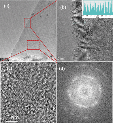 | ||
| Fig. 5 (a) TEM images of a graphene sheet deposited at 240 °C. (b) The edge of the graphene sheet shows presence of a few layers of graphene. In the inset of the figures, the intensity pattern of graphene layers is presented. (c) HRTEM image at the top of the graphene sheet (at red dotted box) showing the presence of a crystalline structure. (d) Fast Fourier transform (FFT) of the graphene sheet, with a set of hexagonal spots in the diffraction pattern. | ||
The synthesized graphene films were isolated by wet etching the Cu foil and transferring them to plastic substrates, which were sufficiently thin to be transparent over the relevant range of wavelengths. Again, diluted HNO3 treatment shows the removal of the remaining Cu and metal etchant; thereby completely removing the effect of the impurities in transparency and sheet resistance. In this experiment the acid concentration was very low which does not damage the graphene surface; rather it has been reported that HNO3 treatment can improve the sheet resistance.9,30 The transparency of graphene film on a plastic or glass substrate can be tuned by controlling the thickness and number of layers. Fig. 6(a) shows the transmittance of a graphene film in comparison with a standard ITO coated substrate. Transferred graphene sheets showed very good transmittance for a wide wavelength range (0.3–2 μm); while ITO shows strong absorption in the region of near and short-wavelength infrared (0.8–2 μm). Transmittance of a thin graphene film was achieved as high as 87% at 550 nm wavelength. Fig. 6(b) shows a photograph of the fabricated flexible transparent electrode with the transferred and deposited graphene film. The transparency of the graphene films are almost similar to that of previous reports on thermal and microwave plasma CVD.26–29 The electrical characterization of the transferred graphene films on plastic substrates was carried out with four probe measurements at room temperature (25 °C). Fig. 6(c) shows the sheet resistance of the graphene films as a function of transmittance at 550 nm wavelength. The sheet resistance reduced with an increase in graphene film thickness; however, transparency of the film also reduced. The sheet resistance of a graphene film with a transmittance of 73% at 550 nm wavelength is obtained as 10.03 kΩ sq−1. The sheet resistance of the low temperature deposited transparent graphene film is still higher than that of thermal CVD graphene; although much better than some other graphene oxide reports.29–32 As the thickness of the graphene film is a few nanometres, the conductivity will be very high. The greater electrical conductivity of the graphene sheet would make it possible to retain adequate lateral electrical conductivity in fabricated electronic devices. The results show possible synthesis of graphene films by the MW-SWP-CVD technique and fabrication of transparent electrodes. The presented low temperature deposition technique can be easily scaled up for metre-scale deposition of transparent graphene films for efficient industrial mass production.
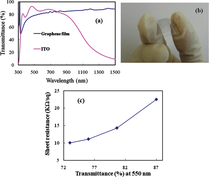 | ||
| Fig. 6 Representation of (a) transmittance of graphene film deposited at 240 °C in comparison to an indium tin oxide (ITO) coated electrode. (b) A photograph of the transferred graphene film on the plastic substrate. (c) Sheet resistance (kΩ sq−1) of the graphene film with variation of % transmittance at 550 nm wavelength. | ||
4. Conclusions
We developed the synthesis of a graphene film by microwave assisted surface wave plasma (MW-SWP) chemical vapor deposition technique at low pressure and temperature using a hydrocarbon gas source. Deposition of few layer graphene films on Cu foil is achieved at a temperature as low as 240 °C. Raman studies showed the deposited carbon films had a graphene structure with a few layers; however defect structures were also present. SEM studies showed uniform deposition of graphene flakes on Cu foil and a continuous transferred film on plastic substrates. TEM studies confirmed the formation of few layer graphene and a HRTEM image showed a crystalline structure with a set of hexagonal spots in the FFT image of a graphene sheet deposited at 240 °C. The nucleation and growth process can be explained by carbon radical formation with hydrogen termination in the microwave plasma, which absorbs continuously onto the Cu surface to form sp2 carbon and eventually a graphene structure. The sheet resistance of a graphene film with a transmittance of 73% at 550 nm wavelength was obtained as 10.03 kΩ sq−1. The presented technique can be easily scaled up for metre-scale deposition of transparent graphene films for efficient industrial mass production.Acknowledgements
The Authors are grateful to M. Noda, S. Adhikari and M. S. Kayastha for their help and discussion during the experiments. Authors are grateful to the Japan Society for Promotion of Science (JSPS) for financial support and fellowship.References
- K. S. Novoselov, A. K. Geim, S. V. Morozov, D. Jiang, Y. Zhang, S. V. Dubonos, I. V. Grigorieva and A. A. Firsov, Science, 2004, 306, 666–669 CrossRef CAS.
- C. Berger, Z. Song, T. Li, X. Li, A. Y. Ogbazghi, R. Feng, Z. Dai, A. N. Marchenkov, E. H. Conrad, P. N. First and W. A. Heer, J. Phys. Chem. B, 2004, 108, 19912 CrossRef CAS.
- Y. Zhang, Y. W. Tan, H. L. Stormer and P. Kim, Nature, 2005, 438, 201–204 CrossRef CAS.
- S. Stankovich, D. A. Dikin, G. H. B. Dommett, K. M. Kohlhaas, E. J. Zimney, E. A. Stach, R. D. Piner, S. T. Nguyen and R. S. Ruoff, Nature, 2006, 442, 282–286 CrossRef CAS.
- A. K. Geim and K. S. Novoselov, Nat. Mater., 2009, 6, 183–191 CrossRef.
- G. Eda, G. Fanchini and M. Chhowalla, Nat. Nanotechnol., 2008, 3, 270–274 CrossRef CAS.
- K. S. Kim, Y. Zhao, H. Jang, S. Y. Lee, J. M. Kim, K. S. Kim, J. H. Ahn, P. Kim, J. Y. Choi and B. H. Hong, Nature, 2009, 457, 706–710 CrossRef CAS.
- X. S. Li, W. W. Cai, J. H. An, S. Kim, J. Nah, D. X. Yang, R. Piner, A. Velamakanni, I. Jung, E. Tutuc, S. K. Banerjee, L. Colombo and R. S. Ruoff, Science, 2009, 324, 1312–1314 CrossRef CAS.
- S. Bae, H. K. Kim, Y. Lee, X. Xu, J. Park, Y. Zheng, J. Balakrishnan, D. Im, T. Lei, Y. Song, Y. Kim, K. Kim, B. Ozyimaz, J. Ahn, B. Hong and S. Iijima, Nat. Nanotechnol., 2010, 5(8), 574–578 CrossRef CAS.
- A. Reina, X. Jia, H. John, D. Nezich, H. Son, V. Bulovic, M. S. Dresselhaus and J. Kong, Nano Lett., 2009, 9(1), 30–35 CrossRef CAS.
- L. S. Mende, A. Fechtenkotter, K. Mullen, E. Moons, R. H. Friend and J. D. MacKenzie, Science, 2001, 293, 1119–1122 CrossRef.
- J. C. Scott, J. H. Kaufman, P. J. Brock, R. Dipietro, J. Salem and J. A. Goitia, J. Appl. Phys., 1996, 79, 2745–585 CrossRef CAS.
- J. Cui, A. C. Wang, N. L. Edleman, J. Ni, P. Lee, N. R. Armstrong and T. J. Marks, Adv. Mater., 2001, 13, 1476–1480 CrossRef CAS.
- X. Wang, L. Zhi and K. Mullen, Nano Lett., 2008, 8, 323–327 CrossRef CAS.
- J. Wu, H. A. Becerril, Z. Bao, Z. Liu, Y. Chen and P. Peumans, Appl. Phys. Lett., 2008, 92, 263302 CrossRef.
- G. Kalita, M. Masahiro, H. Uchida, K. Wakita and M. Umeno, J. Mater. Chem., 2010, 20, 9713–9717 RSC.
- Y. Wang, S. W. Tong, X. F. Xu, B. Özyilmaz and K. P. Loh, Adv. Mater., 2011, 23, 1514–1518 CrossRef CAS.
- Y. Lee, S. Bae, H. Jang, S. Jang, S. E. Zhu, S. H. Sim, Y. Song, B. H. Hong and J. H. Ahn, Nano Lett., 2010, 10, 490–493 CrossRef CAS.
- X. Li, C. W. Magnuson, A. Venugopal, R. M. Tromp, J. B. Hannon, E. M. Vogel, L. Colombo and R. S. Ruoff, J. Am. Chem. Soc., 2011, 133(9), 2816–2819 CrossRef CAS.
- Z. Li, P. Wu, C. Wang, X. Fan, W. Zhang, X. Zhai, C. Zeng, Z. Li, J. Yang and J. Hou, ACS Nano, 2011, 5(4), 3385–3390 CrossRef CAS.
- M. Rusop, S. Adhikari, A. M. M. Omer, S. Adhikary, H. Uchida, T. Jimbo, T. Soga and M. Umneo, Mod. Phys. Lett. B, 2004, 18, 987–1001 CrossRef CAS.
- G. Kalita, S. Adhikari, H. R. Aryal, R. Afre, T. Soga, M. Sharon and M. Umeno, Diamond Relat. Mater., 2008, 17, 1697–1701 CrossRef CAS.
- S. Nakao and H. Sugai, Jpn. J. Appl. Phys., 2007, 46, 1039–1041 CrossRef.
- S. Reich and C. Thomsen, Philos. Trans. R. Soc. London, Ser. A, 2004, 362, 2271–2288 CrossRef CAS.
- A. C. Ferrari, J. C. Meyer, V. Scardaci, C. Casiraghi, M. Lazzeri, F. Mauri, S. Piscanec, D. Jiang, K. S. Novoselov, S. Roth and A. K. Geim, Phys. Rev. Lett., 2006, 97, 187401 CrossRef CAS.
- J. Kim, M. Ishihara, Y. Koga, K. Tsugawa, M. Hasegawa and S. Iijima, Appl. Phys. Lett., 2011, 98, 091502 CrossRef.
- A. Malesevic, R. Vitchev, K. Schouteden, A. Volodin, L. Zhang, G. V. Tendeloo, A. Vanhulse and C. V. Haesendonck, Nanotechnology, 2008, 19, 305604 CrossRef.
- H. M. A. Hassan, V. Abdelsayed, A. E. R. S. Khder, K. M. Abouzeid, J. Terner, M. S. E. Shall, S. I. A. Resayes and A. A. E. Azhary, J. Mater. Chem., 2009, 19, 3832–3837 RSC.
- G. Kalita, K. Wakita and M. Umeno, Phys. E., 2011, 43, 1490–1493 CrossRef CAS.
- A. Kasry, M. A. Kuroda, G. J. Martyna, G. S. Tulevski and A. A. Bol, ACS Nano, 2010, 4, 3839–3844 CrossRef CAS.
- S. Gilje, S. Han, M. Wang, K. L. Wang and R. B. Kaner, Nano Lett., 2007, 7, 3394–3398 CrossRef CAS.
- P. H. Wöbkenberg, G. Eda, D. S. Leem, J. C. de Mello, D. D. C. Bradley, M. Chhowalla and T. D. Anthopoulos, Adv. Mater., 2011, 23, 1558–1562 CrossRef.
| This journal is © The Royal Society of Chemistry 2012 |