Carbon nanotube mat as substrate for ZnO nanotip field emitters†
R. P.
Sugavaneshwar
a,
T.
Nagao
b and
K. K.
Nanda
*a
aMaterials Research Centre, Indian Institute of Science, Bangalore, 12 India. E-mail: suga@mrc.iisc.ernet.in; nanda@mrc.iisc.ernet.in; Fax: +91-80-23607316; Tel: +91-80-2293 2996
bInternational Centre for Materials Nanoarchitectonics (MANA), National Institute for Materials Science, 1-1, Namiki, Tsukuba, Ibaraki, Japan. E-mail: taadaki.NAGAO@nims.go.jp
First published on 31st January 2012
Abstract
We have reported the synthesis of ZnO nanotips on a multi walled carbon nanotube (MWCNT) mat by a vapour transport process. This combination of ZnO nanotips and a MWCNT mat exhibit ideal field emission behaviour. The turn on field and threshold field is found to be 0.34 and 1.5 V μm−1, respectively. The low threshold field is due to the good adherence of the ZnO nanotips on the MWCNT mat. The field enhancement factor is found to be 5 × 10² which is in agreement with the intrinsic field emission factor of ZnO nanotips. The emission current is found to be highly stable even at moderate vacuum.
A quest is on to obtain suitable materials, morphology and/or a combination of substrates and materials with a low threshold voltage for field emission (FE) applications. It has been shown that the suitable substrates are essential for a material to exhibit the best field emission behavior.1–3 The best results reported so far are the field emission of multi-wall carbon nanotubes (MWCNT) on carbon cloth. An electric field of 0.34 V μm−1 is required to obtain an emission current density of 1 mA cm−2.1,4 However, the stability of MWCNT under low vacuum conditions is a concern as adsorption and desorption gases on the tip of MWCNTs leads to instability in emission.5
ZnO has demonstrated the richest nanostructures of all known materials. In recent years tremendous progress has been made in ZnO based FE devices as they are thermally stable and intrinsically oxidation resistant.6–8 In particular, the FE behaviour of ZnO needle/nanopencil like structures have been reported to be the best9–12 because of the increase in the effective electric field at their tips.13 Several groups have successfully synthesized ZnO nanostructures on MWCNTs to obtain an improved field emission performance. Here, we summarize the exceptional results reported until today. A fairly low turn-on field (defined as an E which is required to produce J of 10 μA cm−2) and the low threshold field (defined as E where J is 1 mA cm−2) of 2.5 and 4.0 V μm−1, respectively has been achieved for ZnO nanoneedles on a silicon wafer.9 ZnO nanopencils on a silicon wafer show a low turn-on field of 3.7 V μm−1 and a threshold field of ∼4.6 V μm−1.10 The emission at the low field is attributed to the sharp tip on the nanoneedles/nanopencils. There are reports on the FE studies of ZnO nanostructures coated over carbon nanostructures. ZnO nanoparticles coated over MWCNT show a threshold field of 4.0 V μm−1.14 A threshold field of 3.1 V μm−1 has been reported for ZnO nanowires grown on vertically aligned carbon nanofibers,15 while it is 2.3 V μm−1 for ZnO nanostructures grown on a screen printed MWCNT-film.16 The best results reported up to today are by Ren and co-workers.17 A threshold field of 0.7 V μm−1 has been achieved and the low threshold field is due to the combined effect of the geometry of ZnO and carbon cloth.17 In most of the cases, ZnO nanostructures are grown on the surface of the silicon or nanotubes or nanofibers for the FE studies. However, there are no reports on the FE behavior of ZnO nanoneedles on a MWCNT mat.
Here in this communication we report the synthesis of ZnO nanotips on a MWCNT mat and their FE behavior. The MWCNT mat is synthesized by a one-step pyrolysis technique. MWCNT-ZnO heterostructures are fabricated by growing ZnO nanotips on top of a MWCNT mat by a vapour transport technique. A turn-on field of 0.34 V μm−1 and a threshold field of 1.5 V μm−1 was achieved for 1.0 mA cm−2 which is better than the other MWCNT-ZnO based results. The improved FE is attributed to the sharp tip morphology at the apex of ZnO nanorods and the better adhesion between MWCNT and ZnO. The field enhancement factor is found to be 5 × 10² which is in agreement with the intrinsic field emission factor of ZnO nanotips. The emission current is highly stable even at 10−5 Torr. We have also shown that the morphology of the ZnO nanotips is stable after the field emission studies
Experimental
The ZnO nanotips on the MWCNT mat were prepared by two-steps. First, MWCNTs are synthesized by a simple pyrolysis already reported in the literature.18 Benzene is taken as a source of carbon and ferrocene as a source of iron that acts as the catalyst for the growth of MWCNT. A mixture of 18 mg of ferrocene and 2 ml of benzene is taken in a quartz tube closed at one end. The other end of the quartz tube is connected to a rubber bladder to collect the residual gases. The entire assembly is placed inside the furnace and heated up to the desired pyrolysis temperature 1100 °C and the reaction is allowed for 120 min after it reaches the desired set temperature.After the reaction is over, aligned MWCNT formed on a p-type Si substrate which is kept in the middle of the quartz tube. The MWCNT-ZnO heterostructure was formed by making 10 mg of Zn powder (S.D fine 99.5%) into a compact mass and placing a Si substrate above it in the centre of a quartz boat which is placed inside the alumina tube on a single zone furnace. The MWCNT mats grown on the Si substrate are placed at nearby distances from the source and heated to 650 °C for one hour under an argon gas flow of 110 sccm (standard cubic centimetres per minute). Due to the negligible solid solubility of Zn in Si, the Zn does not dissolve in Si and therefore the Zn vapours which are generated during the experiment are transported under argon flow to nearby regions, forming ZnO nanotips on the MWCNT/Si.
After the experiments, the products are analysed by a Quanta 200 scanning electron microscopy (SEM) and the FE studies are carried out using a custom-built measurement system. FE properties were investigated using a simple diode configuration in a high vacuum chamber at a pressure of 8 × 10⁻⁷ Torr. The Si/MWCNT/ZnO nanotip cathode was placed on an aluminium sample stage, and beneath an indium tin oxide/glass anode, separated by an insulating spacer whose thickness is 50 μm. The measured emission area was 36 mm2
Results and discussion
Fig. 1(a)–(d) show the low and high magnification SEM images revealing ZnO nanotips grown on a MWCNT mat. The growth of ZnO nanotips on the MWCNT mat is found to be quite dense. The low magnification and tilted view of the ZnO nanotips in Fig. 1(c) and (d) show that they are almost uniform in length. The length of the ZnO nanotips grown on top of the MWCNTs is ∼10 μm and the diameter of the ZnO nanotips varied from 100 nm in the bottom to 20 nm toward the tip. HRTEM (High Resolution Transmission Electron Microscope) and SAED (Selected Area Electron Diffraction) as shown in Fig. 1(e) and (f) indicate a (0002) growth direction of the ZnO with a d spacing of 0.2628 nm.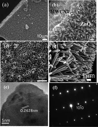 | ||
| Fig. 1 (a) Low and (b) high magnification SEM images of the MWCNT/ZnO nanotips. (c) top and (d) tilted view of ZnO tips. (e) HRTEM image of the tip of the needle. Growth direction as indicated by the arrow is (0002). (f) SAED of the ZnO nanotips. | ||
| J = A(β2V2/ϕd2)exp (−Bϕ3/2d/βV), |
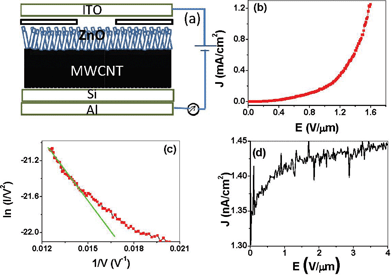 | ||
| Fig. 2 (a) Schematic of the field emission set up. (b) I–V curve for MWCNT-ZnO and (c) the corresponding FN plot. (d) I–V curve for silicon substrate on Al. | ||
The effective field enhancement factor β of the ZnO tip can be calculated from the slope of the FN plot if the work function of the emitter is known. Using reported values for the work functions of 5.3 eV for ZnO, the average field enhancement factor of MWCNT-ZnO was found to be ∼5 × 10². The intrinsic field enhancement factor of an individual nanowire is approximately proportional to the aspect ratio of 0.72l/r, where l and r are the length and tip radius of nanowire, respectively.19,20 Since the length of the ZnO nanowires is ∼10 μm and the tip radius is ∼10 nm, the intrinsic field enhancement factor of the ZnO nanotips is calculated to be ∼720. This indicates that the field enhancement factor obtained from the experimental results is consistent with the intrinsic field enhancement factor.
It is well known that the emission current density is strongly dependent on the work function of an emitter surface and the radius of curvature of the emitter apex,21 and emitters grown directly on conducting substrates result in the formation of robust electrical contacts during growth.22 In order to investigate the electrical connectivity between MWCNT and ZnO, we have studied the current (I)–voltage (V) characteristics of the ZnO nanotip grown on a MWCNT mat with the configuration shown in Fig. 3(a) and the IV characteristic is shown in Fig. 3(b). The IV characteristic is linear indicating that the heterostructures are ohmic in nature and the resistance is estimated to be 30 Ω. ZnO and MWCNTs form an ohmic contact23,24 because MWCNTs have a lower work function (4.5–5.0 eV)25,26 than n-type ZnO (5.3–5.4 eV).17
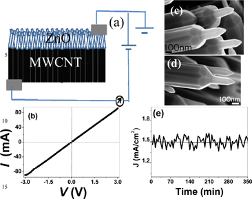 | ||
| Fig. 3 (a) Schematic of the I–V setup. (b) I–V curve for MWCNT-ZnO structures. High magnification SEM image of the ZnO tips (c) before and (d) after field emission studies. (e) Emission stability of MWCNT-ZnO structures at 3 × 10⁻⁵ Torr. | ||
Emission stability is one of the properties that needs to be evaluated for practical applications. SEM images as shown in Fig. 3(c) & 3(d) taken before and after the field emission studies reveal no change in the morphology that corroborates the high emission stability of MWCNT-ZnO structures. Shown in Fig. 3(e) is the emission current density with respect to different time at an applied voltage of 2.7 V μm−1. It may be noted that the pressure of the system was 3 × 10⁻⁵ Torr. As can be seen from this investigation, the emission stability of the ZnO nanotips is excellent. We have also summarised the threshold field Vth for ZnO, WO3 and CdS in Table 1. It is interesting to note that enhanced performance has been reported when the materials are grown on a carbon based substrate, suggesting that growing on a carbon based substrate might lead to improved performance.
| Materials | V th (V μm−1) | Reference |
|---|---|---|
| ZnO | ||
| Nanoneedles on Si | 4.0 | 9 |
| Nanoneedles on Si | 4.6 | 10 |
| Nanoparticles coated over CNTs | 4.0 | 12 |
| Nanowires on carbon nanofibers14 | 3.1 | 14 |
| Nanomultipode on MWCNT film15 | 2.3 | 15 |
| Nanowires on carbon cloth | 0.7 | 16 |
| Nanotips on MWCNT | 1.5 | This work |
| WO3 | ||
| Nanowires on Si | 6.5 (0.014 mA cm−2) | 27 |
| Nanobrushes on Si | 8.9(0.14 mA cm−2) | 28 |
| Nanowire on ITO glass | 9.1 | 29 |
| Whisker Arrays on Si | 6.5 | 30 |
| Nanowires on carbon papers | 3.3 | 31 |
| CdS | ||
| Nanoparticles on SWNT film | 8.5(0.5 mA cm−2) | 32 |
| Nanostructures on Si | 20.5 | 33 |
Conclusion
We have reported the growth of ZnO nanotips on a MWCNT mat and one of the best combinations reported for FE studies. The low threshold voltage and large emission current density is mainly attributed to the sharp nanotip structure at the end of the ZnO nanowires and the coherent formation of the MWCNT-ZnO heterostructure. The enhancement factor was found to be moderate but in agreement with the intrinsic field enhancement factor of ZnO nanotips. The emission current is found to be highly stable. We believe that our work will motivate researchers to use MWCNT mats as substrates for different investigations. Over all, carbon based substrates are appropriate for improved FE performance of most of the materials.Acknowledgements
One of the authors (RPS) acknowledges financial support from National Institute of Materials Science (NIMS), Tsukuba, Japan for conducting the experiments at NIMS. The authors also acknowledge CSIR for the financial support and Grant-in-aid program from the ministry of education, culture, sports, and technology (MEXT).References
- S. Shih-Chen, C. Chia-Fu, C. Surojit, C. Kuei-Hsien and C. Li-Chyong, Appl. Phys. Lett., 2005, 87, 073109 CrossRef.
- M. Hirohiko, H. Masaaki, T. Chiaki and Y. Hiroyuki, Appl. Phys. Lett., 2000, 76, 1776–1778 CrossRef.
- C. S. Chang, S. Chattopadhyay, L. C. Chen, K. H. Chen, C. W. Chen, Y. F. Chen, R. Collazo and Z. Sitar, Phys. Rev. B: Condens. Matter, 2003, 68, 125322 CrossRef.
- S. H. Jo, D. Z. Wang, J. Y. Huang, W. Z. Li, K. Kempa and Z. F. Ren, Appl. Phys. Lett., 2004, 85, 810–812 CrossRef CAS.
- J. Wang, X. Zhang, W. Lei, M. Xiao, Y. Cui, Y. Di and F. Mao, J. Vac. Sci. Technol., B: Microelectron. Nanometer Struct.–Process., Meas., Phenom., 2007, 25, 615–617 CrossRef CAS.
- A. Wei, X. W. Sun, C. X. Xu, Z. L. Dong, M. B. Yu and W. Huang, Appl. Phys. Lett., 2006, 88, 213102 CrossRef.
- Q. Wan, K. Yu, T. H. Wang and C. L. Lin, Appl. Phys. Lett., 2003, 83, 2253–2255 CrossRef CAS.
- J. J. Liu, M. H. Yu and W. L. Zhou, Appl. Phys. Lett., 2005, 87, 172505 CrossRef.
- Y. B. Li, Y. Bando and D. Golberg, Appl. Phys. Lett., 2004, 84, 3603–3605 CrossRef CAS.
- R. C. Wang, C. P. Liu, J. L. Huang, S. J. Chen, Y. K. Tseng and S. C. Kung, Appl. Phys. Lett., 2005, 87, 013110 CrossRef.
- X. Fang, Y. Bando, U. K. Gautam, C. Ye and D. Golberg, J. Mater. Chem., 2008, 18, 509–522 RSC.
- X. Hai Jun, C. Yu Fei, S. Lei, L. De Yao and S. Xiao Ming, J. Appl. Phys., 2010, 108, 114301 CrossRef.
- C. X. Xu and X. W. Sun, Appl. Phys. Lett., 2003, 83, 3806–3808 CrossRef CAS.
- J. M. Green, L. Dong, T. Gutu, J. Jiao, J. F. Conley and Y. Ono, J. Appl. Phys., 2006, 99, 094308 CrossRef.
- C. Li, Y. Zhang, M. Mann, P. Hiralal, H. E. Unalan, W. Lei, B. P. Wang, D. P. Chu, D. Pribat, G. A. J. Amaratunga and W. I. Milne, Appl. Phys. Lett., 2010, 96, 143114 CrossRef.
- K. Yu, Y. S. Zhang, F. Xu, Q. Li, Z. Q. Zhu and Q. Wan, Appl. Phys. Lett., 2006, 88, 153123 CrossRef.
- D. Banerjee, S. H. Jo and Z. F. Ren, Adv. Mater., 2004, 16, 2028–2032 CrossRef CAS.
- P. Mahanandia and K. K. Nanda, Appl. Phys. Lett., 2008, 93, 063105 CrossRef.
- C. J. Edgcombe and U. Valdrè, Solid-State Electron., 2001, 45, 857–863 CrossRef CAS.
- C. J. Edgcombe and U. Valdrè, J. Microsc., 2001, 203, 188–194 CrossRef CAS.
- N. S. Xu and S. E. Huq, Mater. Sci. Eng., R, 2005, 48, 47–189 CrossRef.
- T. Hiraoka, T. Yamada, K. Hata, D. N. Futaba, H. Kurachi, S. Uemura, M. Yumura and S. Iijima, J. Am. Chem. Soc., 2006, 128, 13338–13339 CrossRef CAS.
- J. G. Ok, S. H. Tawfick, K. A. Juggernauth, K. Sun, Y. Zhang and A. J. Hart, Adv. Funct. Mater., 2010, 20, 2470–2480 CrossRef CAS.
- M. Yo-Sep, B. Eun Ju, K. Un Jeong, P. Wanjun and H. Cheol Seong, Appl. Phys. Lett., 2006, 89, 113116 CrossRef.
- M. Shiraishi and M. Ata, Carbon, 2001, 39, 1913–1917 CrossRef CAS.
- H. Ago, T. Kugler, F. Cacialli, W. R. Salaneck, M. S. P. Shaffer, A. H. Windle and R. H. Friend, J. Phys. Chem. B, 1999, 103, 8116–8121 CrossRef CAS.
- W. C. Tsai, S. J. Wang, C. L. Chang, C. H. Chen, R. M. Ko and B. W. Liou, EPL (Europhysics Letters), 2008, 84, 16001 CrossRef.
- A. Yella, U. K. Gautam, E. Mugnaioli, M. Panthofer, Y. Bando, D. Golberg, U. Kolb and W. Tremel, CrystEngComm, 2011, 13, 4074–4081 RSC.
- K. Huang, Q. Pan, F. Yang, S. Ni and D. He, Mater. Res. Bull., 2008, 43, 919–925 CrossRef CAS.
- S. Wang, Y. He, X. Fang, J. Zou, Y. Wang, H. Huang, P. M. F. J. Costa, M. Song, B. Huang, C. T. Liu, P. K. Liaw, Y. Bando and D. Golberg, Adv. Mater., 2009, 21, 2387–2392 CrossRef CAS.
- L. Li, Y. Zhang, X. Fang, T. Zhai, M. Liao, X. Sun, Y. Koide, Y. Bando and D. Golberg, J. Mater. Chem., 2011, 21, 6525–6530 RSC.
- L. Jungwoo, L. Wonjoo, P. Taehee, L. Jaeseung, P. Eunkyung, L. Donghwan, L. Jongtaek and Y. Whikun, 201028C2B43–C42B46.
- T. Zhai, X. Fang, Y. Bando, Q. Liao, X. Xu, H. Zeng, Y. Ma, J. Yao and D. Golberg, ACS Nano, 2009, 3, 949–959 CrossRef CAS.
Footnote |
| † Electronic Supplementary Information (ESI) available. See DOI: 10.1039/c2ra00001f/ |
| This journal is © The Royal Society of Chemistry 2012 |