Self-assembly of two-dimensional nanostructures of linear regioregular poly(3-hexylthiophene)
Zai
Yu
ab,
Han
Yan
a,
Kun
Lu
a,
Yajie
Zhang
a and
Zhixiang
Wei
*a
aNational Center for Nanoscience and Technology, Beijing, 100090, China. E-mail: weizx@nanoctr.cn; Fax: +86 10 62656765; Tel: +86 10 82545565
bAcademy for Advanced Interdisciplinary Studies, Peking University, Beijing, 100871, China
First published on 4th November 2011
Abstract
Two dimensional poly(3-hexylthiophene) (P3HT) nanosheets were prepared by evaporation of a diluted mixture of solvent. The dimension and size of the nanostructures was controlled by tuning the good-to-poor solvent ratio. The morphology and structure of the nanosheets were fully characterized. Atomic Force Microscopy (AFM) characterization showed the nanosheets were lamellar structures with a thickness of about 3–5 nm of a single layer. The anisotropic arrangement of P3HT was clearly defined by selected area electron diffraction. In the nanostructures, P3HT adopted the edge on orientation with the π–π stacking direction parallel to the substrate and the alkyl side chains perpendicular to the substrate. Single nanosheet showed a typical anisotropic charge carrier transport property.
Introduction
As a promising semiconductive material, regioregular poly(3-hexylthiophene) (P3HT) has been widely used in organic electronics, such as light emitting devices,1–2 solar cells3–5 and field effect transistors6–8 for its excellent electrical and optical properties. Both the dimension and crystal structures of the polymer affect the charge transport properties and finally influence the device performance.9–10 Therefore, controlling the dimension and structures of the polymer crystals, understanding the crystalline process is of great importance for obtaining high device performance.Two dimensional (2D) materials have shown potential applications in highly integrated devices.11–13 For example, graphene have been extensively investigated as building blocks in nanodevices due to their intriguing opto-electrical and physical properties.14–16 Construction 2D nanostructures of other functional materials is of great importance for their potential applications. For example, millimetre-sized 2D organic single crystals were prepared.17 And using the monolayer crystals as a semiconducting layer, high performance organic field-effect transistors was obtained with a mobility up to 1.0 cm2 V−1 s−1. And recently, 2D polyaniline microplate was fabricated, which showed anisotropic electron transport properties.18
Strong π–π interactions between planar molecular backbones make it favorable for P3HT to form crystalline nanostructures. Until now, P3HT nanostructures have been prepared under different self-assembly procedures. For one dimensional (1D) nanostructures, polycrystalline P3HT nanowires have been fabricated by recrystallization19–20 and slow solvent evaporation.21 even more complicated hyper-branched structures can be fabricated by controlled evaporation of a blend solvent.22 Single crystals of microwires were prepared using the self-seeding technique23, and microneedles were grown by solvent–vapor annealing.24 Recently, 2D P3HT nanostructures were also successfully prepared. Polycrystalline P3HT nanoribbons were fabricated by crystallization from the solution.25 However, constructing 2D single-crystalline P3HT nanostructures is still a challenge. Herein, we focused on the construction of 2D P3HT nanostructures.
Slow solvent evaporation was found to be an efficient way to fabricate P3HT nanowires, and different solvent had been used, such as chloroform and chlorobenzene, where P3HT had good solubility. However the evaporation of a good solvent contains P3HT only produced 1D nanostructures. The introduction of poor solvent was commonly used to prepare conducting polymer nanostructures. In this study, we prepared 2D P3HT single crystals by evaporation of a diluted mixture of solvent, a combination of poor solvent and slow evaporation. The nanostructures were obtained under two self-assembly processes: (i) transferring the polymer from a good solvent to a poor solvent, which was accompanied with a nucleation process; (ii) a slow evaporation process then results in the growth of the nanostructures (Fig. 1).
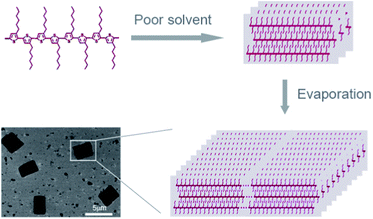 | ||
| Fig. 1 Schematic representation of the self-assembly process of P3HT nanostructures. | ||
The size of the nanostructures can be controlled by tuning the good-to-poor solvent ratio.
Experimental
Preparation of P3HT nanostructures
Regioregular P3HT (M∼25000, regioregularity greater than 98.5%), was purchased form Aldrich and used as received. Tetrahydrofuran (THF) and methanol was purchased form Sinopharm Chemical Reagent Co. Ltd. and distilled prior to use.A schematic representation of the preparation process of P3HT nanostructures is showed in Fig. 2a. P3HT was firstly dissolved in THF with a concentration of 0.05 mg mL−1. 500 μL of this solution was fast injected into 5 mL mixture of solvent of methanol and THF, followed by immediate mixing. The final concentration of the molecule was about 0.005 mg mL−1. A drop of this solution was deposited onto the silicon substrate in a small box. Then the box was covered to self-assemble at room temperature. It takes several hours for the solvent to evaporate. Lamellar crystals were formed on the substrate after the solvent was evaporated. The methanol ratio in the mixture of solvent was changed from 20% to 100%.
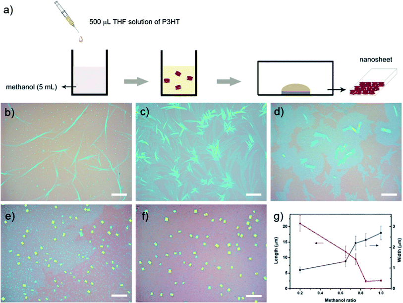 | ||
| Fig. 2 a) Schematic representation of the preparation process of P3HT nanostructures. Optical microscopy images of P3HT nanostructures fabricated from evaporation of a mixed solvent with different methanol ratio: b) 20%; c) 60%; d) 70%; e) 80%; f) 100%; g) diagram of crystal size vs.methanol ratio. Scale bars: 20 μm. | ||
Characterization of P3HT nanostructures
The morphology of the nanostructures was characterized by scanning electron microscopy (SEM, Hitachi S–4800, Japan), transmission electron microscopy (TEM, Tecnai G2 F20 U-TWIN, FEI Co., USA) and optical microscopy (Leica DM4000M). The height of the crystal was measured by atomic force microscopy (AFM, Dimensional 3100, Veeco, USA). UV-vis absorption spectra and PL spectra of P3HT solution were recorded using a UV-vis spectrophotometer (Lambda 950, Perkin-Elmer, USA) and photoluminescence spectrophotometer (LS 55 Perkin-Elmer, USA), respectively. The crystalline structures were measured by X-ray diffraction (XRD, D/max-rA 12 kW). Current voltage (I–V) characteristics were recorded with a keithley 4200-SCS and a Micromanipulator 6150 probe station in a clean and shielded box at room temperature.Electrical transport measurement
Au top-contact devices of a single P3HT nanosheet were constructed for electrical characterization. The sample were grown on heavily doped n-type silicon substrates with a 300 nm capped layer of SiO2, and was kept under vacuum for 48 h at room temperature to remove the residue solvent. Au layers were transferred onto the nanosheet as electrodes.10Results and discussion
P3HT can be well dissolved in THF at room temperature and has poor solubility in methanol. The preparation of P3HT nanostructures first required transferring P3HT molecules from a good solvent to a poor solvent by adding a small volume of THF solution of P3HT to a large volume mixture of solvent of methanol and THF. The as prepared mixed solution was then dropped onto a substrate to self-assemble nanostructures. Slightly increasing the poor solvent ratio changed P3HT nanostructures from nanoribbons to rectangle nanosheets.As shown in Fig. 2, it was found that increasing the poor solvent ratio accompanied with a decrease of the crystal size. At low methanol ratio (e.g. 20% in Fig. 2b) long ribbon-like crystals were formed with the length of tens of micrometres and the width of about 1 μm. Then the length of the ribbons decreased as an increase of methanol ratio to 60% (Fig. 2c). When the methanol ratio was increased to 70%, 2D nanosheets were formed and the crystal length decreased to about 10 μm. Further increase in the ratio of methanol produced nanosheets with further decreased crystal size (Fig. 2d). Nanosheets obtained at a methanol ratio of 80% and 100% are of the similar size, but 100% methanol ratio led to more uniformed size (Fig. 2e and 2f). P3HT nanosheets with an average length of 3.5 μm and width of 2.5 μm were prepared with 100% methanol. However, Only irregular aggregates were observed if the THF solution is deposited under the same experimental conditions. Fig. 2g shows the crystal size varied with different methanol ratio. A decrease of the length was resulted from the increased nucleus-to-free-molecule ratio in the two-step self-assembly process. And the slightly increase of the width was ascribed to the improved π–π interaction among the polymer backbones as the poor solvent ratio increased.
To study the formation mechanism of the nanostructures, the absorption and emission spectrum of P3HT solutions were recorded after adding P3HT to the mixture of solvent with different methanol ratio (Fig. 3). Only one absorption peak at 435 nm was observed in THF and 20% methanol, which indicated that the polymer chains were well-dissolved. At a methanol ratio of 30%, additional absorption peaks at 515, 555, and 610 nm appeared which was attributed to the extension of conjugation length with improved π–π stacking of the P3HT chains.26 As methanol ratio was further increased these low-energy peaks increased gradually while the peak at 435 nm decreased. Moreover, fluorescent quenching was observed from the emission spectrum with an increase of methanol ratio, which was also resulted from the P3HT aggregation.27 As a result, we suggest that methanol acted as a poor solvent and induced the aggregation of P3HT, which was a key factor to prepare 2D P3HT nanostructures.
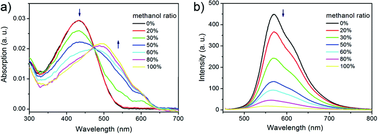 | ||
| Fig. 3 a) UV-vis and b) PL spectrum of P3HT solutions with different methanol ratios. | ||
The formation of 2D P3HT nanostructures was ascribed to the combination of the poor solvent and slow evaporation. In this self-assembly process, both π–π interaction and van der Waals interactions played important roles. In the first process, P3HT was transferred from a good solvent into a poor solvent where the polymer had limited solubility. In this situation, van der Waals interactions and π–π stacking interactions between the P3HT molecules suppressed the solvent effect and nucleus formed. In the second process, evaporation of the solvent resulted in further aggregation, which occurred not only along the π–π stacking direction but also the main chain direction driven by van der Waals interactions, therefore led to the formation of 2D nanostructures.
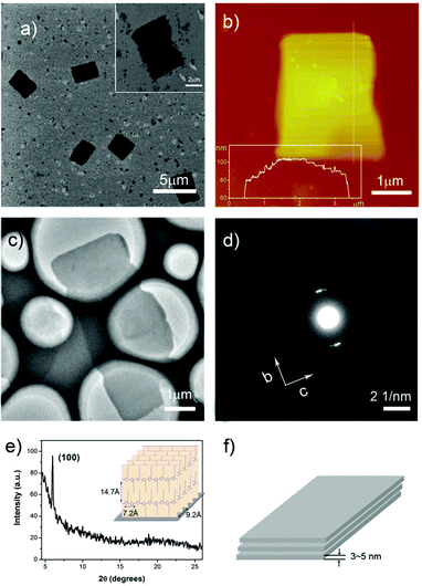
To study the arrangement of P3HT molecules in the nanostructures, further structure characterizations were carried out. Fig. 4 showed the structure analysis of the nanosheets fabricated at 70% methanol. An optical microscopy image of several nanosheets was presented in Fig. 4a. Fig. 4b showed the scanning electron microscopy (SEM) image of a typical nanosheet. AFM image and section analysis of a single nanosheet was also recorded (Fig. 4c, 4d). The height image showed the thickness of the nanosheet was about 70 nm. In the inset of Fig. 4d, the clearly presented stages indicated that the crystals possessed the lamellar structures with a 3-5 nm thickness of a single layer. The thickness of a single layer was quite similar to the thickness of P3HT nanowhiskers, corresponding to two or three P3HT monolayers.28Transmission electron microscopy (TEM) and selected area electron diffraction (SAED) of the nanostructure was also recorded (Fig. 4e, 4f). The patterns showed a d-spacing of 4.6 Å from the (020) reflection of the π–π stacking direction (b axis) and 3.6 Å from the (002) reflection of the polymer chain direction (c axis).
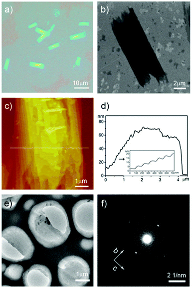 | ||
| Fig. 4 Structure characterization of P3HT nanostructures prepared at 70% methanol: a) optical microscopy image of the nanosheets; b) SEM image of a typical nanosheet; c) AFM height image and d) section analysis of a nanosheet; e) TEM image and f) SAED patterns of nanosheets. | ||
We also studied the structure and the arrangement of P3HT molecules of the nanosheets prepared at methanol ratio of 100%. Fig. 5a showed SEM image of the ordered rectangle nanosheets and the size were uniform. A high magnifications SEM image presented a typical nanosheet. Fig. 5b showed AFM height image and section analysis of the nanosheet. The thickness of the crystal was about 100 nm and the stages on the edge of the structure were also clearly presented, which indicated that the nanosheets prepared at methanol ratio of 100% were also lamellar crystals with a thickness of a 3–5 nm thickness of each layer. Compared to the crystals prepared at methanol ratio of 70%, the height of the crystals was increased because of the improved alkyl chain interaction at high methanol ratio. TEM and SAED of the nanostructure was also recorded (Fig. 5c, 5d). A d-spacing of 4.6 Å from the (020) reflection of the π–π stacking direction (b axis) and 3.6 Å from the (002) reflection of the polymer chain direction (c axis) were presented in diffraction the patterns. Fig. 5e showed XRD profiles of the nanosheets grown on a silicon wafer. A diffraction peak presented at 2θ ≈ 5.9° (d = 14.7 Å), corresponding to the (100) reflection. From these results, it is possible to deduce that the nanosheet had an orthorhombic crystal unit cell with lattice constants a∼14.7 Å, b∼9.2 Å, and c∼7.2 Å. A schematic illustration of the polymer chain stacking in the crystal was given in the inset of Fig. 5e. The molecules adopted the edge on orientation with the π–π stacking direction parallel to the substrate and the alkyl side chains perpendicular to the substrate. Fig. 5f showed a schematic representation of the lamellar structure of the nanosheet. In summery, when methanol ratio was less than 70%, P3HT molecules aligned with π–π stacking direction perpendicular to the long axis of the nanostructure; and when methanol ratio was more than 80%, the π–π stacking direction was parallel to the long axis of the nanostructure. This was resulted from the decrease of the length and increase of the width as more methanol was added.
 | ||
| Fig. 5 Structure characterization of P3HT nanostructures prepared at 100% methanol: a) SEM image of the nanosheets; b) AFM height image and section analysis of a typical nanosheet; c) TEM image and d) SAED patterns of a nanosheet; e) XRD profiles and schematic illustration of the assembly of the P3HT chains in the nanosheet. f) Schematic illustration of the lamellar structure of the crystal. | ||
In most cases, the d-spacing of the a axis of P3HT was reported to be around 16 Å, which was assigned as phase 1.29–31 The side chain interdigitation was minimal in this situation. While in phase 2, side chain interdigitation was commonly observed.30–32 For poly(3-alkylthiophene)s (P3ATs), the π–π stacking distance was varied with different materials. In general, the π–π stacking distance of phase 2 was larger than that of phase 1 (∼3.9 Å).33–37 For example, a π–π stacking distance of 4.7 Å and 4.85 Å was also reported for poly(3-butylthiophene) and poly(3-octylthiophene).38–39 In our study, the d-spacing of a axis indicated the interdigitation of the alkyl side chain and a relatively larger π–π stacking distance was obtained, which indicated that P3HT crystallized to nanosheets in the form of phase 2.
In order to determine the structure-property relationship, electrical transport studies on P3HT nanostructures were studied (Fig. 6). Au top-contact devices were fabricated to determine the anisotropic transport properties of a nanosheet. The device in Fig. 6a was to test the electrical transport property along the polymer main chain direction (c axis) and the device in Fig. 6b was to test the charge carrier transport property along the π–π stacking direction (b axis). The nanosheets showed anisotropic transport properties. The conductivity of the π–π sacking direction was higher than that of the main chain direction, but the conductivities were relatively lower compared to other report.40 This might resulted by the long π–π stacking distance of 4.6 Å, which was disadvantageous to the interchain charge hopping. As a result, the fabricated FET devices showed poor performance. In our experiment, there were still a few factors that were not optimized, for example, the lack of monolayer dielectric and the influence of water and oxygen at atmosphere. The crystals tended to huddle together instead of spread out on the substrate that was treated with octadecyltrichlorosilane. Moreover, the performance of FET devices base on P3HT films was decreased very fast at atmosphere.41 Therefore, further optimization of the device structure is required.
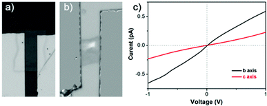 | ||
| Fig. 6 a), b) Optical microscopy image of Au top-contact devices constructed from a P3HT nanosheet; b) I–V curve of the nanosheet. | ||
Conclusions
In conclusion, single crystalline 2D P3HT nanosheets were prepared by evaporation of a diluted mixture of solvent. Both the poor solvent and evaporation process were key factors to the formation of the nanostructures. The dimension and size of the nanostructures was controlled by tuning the good-to-poor solvent ratio. The nanosheets are lamellar crystals with a thickness of 3–5 nm of each layer. In the nanostructures, P3HT adopted the edge on orientation with the π–π stacking direction parallel to the substrate and the alkyl side chains perpendicular to the substrate. Electrical transport characterization of the nanosheet showed anisotropic transport properties. This work provides a method to fabricate 2D P3HT nanostructures and was potentially a useful technique for organizing 2D nanostructures into highly integrated devices.Acknowledgements
We acknowledge the financial support of the National Natural Science Foundation of China (Nos. 20974029, 91027031), The Ministry of Science and Technology of China (Nos. 2006- CB932100, 2009CB930400), and the Chinese Academy of Sciences (KJCX2-YW-M13). We thank the helpful discussions with Prof. M. He, National Center for Nanoscience and Technology of China on SAED and XRD results.References
- R. Osterbacka, G. Juska, K. Arlauskas, A. J. Pal, K. M. Kalman and H. Stubb, J. Appl. Phys., 1998, 84, 3359–3363 CrossRef CAS.
- J. Pei, W. L. Yu, W. Huang and A. J. Heeger, Macromolecules, 2000, 33, 2462–2471 CrossRef CAS.
- E. Hosono, S. Fujihara, I. Honna and H. S. Zhou, Adv. Mater., 2005, 17, 2091 CrossRef CAS.
- G. Li, V. Shrotriya, Y. Yao, J. S. Huang and Y. Yang, J. Mater. Chem., 2007, 17, 3126–3140 RSC.
- S. H. Park, A. Roy, S. Beaupre, S. Cho, N. Coates, J. S. Moon, D. Moses, M. Leclerc, K. Lee and A. J. Heeger, Nat. Photonics, 2009, 3, 297 CrossRef CAS.
- H. G. O. Sandberg, G. L. Frey, M. N. Shkunov, H. Sirringhaus, R. H. Friend, M. M. Nielsen and C. Kumpf, Langmuir, 2002, 18, 10176–10182 CrossRef CAS.
- J. F. Chang, B. Q. Sun, D. W. Breiby, M. M. Nielsen, T. I. Solling, M. Giles, I. McCulloch and H. Sirringhaus, Chem. Mater., 2004, 16, 4772–4776 CrossRef CAS.
- H. Dong, C. Wang and W. Hu, Chem. Commun., 2010, 46, 5211–5222 RSC.
- D. H. Kim, Y. D. Park, Y. S. Jang, H. C. Yang, Y. H. Kim, J. I. Han, D. G. Moon, S. J. Park, T. Y. Chang, C. W. Chang, M. K. Joo, C. Y. Ryu and K. W. Cho, Adv. Funct. Mater., 2005, 15, 77–82 CrossRef CAS.
- Q. X. Tang, Y. H. Tong, H. X. Li, Z. Y. Ji, L. Q. Li, W. P. Hu, Y. Q. Liu and D. B. Zhu, Advanced Materials, 2008, 20, 1511 CrossRef CAS.
- Y. L. Lei, Q. Liao, H. B. Fu and J. N. Yao, J. Phys. Chem. C, 2009, 113, 10038–10043 CAS.
- Z. Y. Tang, Z. L. Zhang, Y. Wang, S. C. Glotzer and N. A. Kotov, Science, 2006, 314, 274–278 CrossRef CAS.
- H. Sirringhaus, P. J. Brown, R. H. Friend, M. M. Nielsen, K. Bechgaard, B. M. W. Langeveld-Voss, A. J. H. Spiering, R. A. J. Janssen, E. W. Meijer, P. Herwig and D. M. de Leeuw, Nature, 1999, 401, 685–688 CrossRef CAS.
- K. S. N. A. K. Geim, Nat. Nanotechnol., 2010, 5, 755–755 CrossRef.
- X. L. Li, X. R. Wang, L. Zhang, S. W. Lee and H. J. Dai, Science, 2008, 319, 1229–1232 CrossRef CAS.
- K. S. Novoselov, A. K. Geim, S. V. Morozov, D. Jiang, Y. Zhang, S. V. Dubonos, I. V. Grigorieva and A. A. Firsov, Science, 2004, 306, 666–669 CrossRef CAS.
- L. Jiang, H. Dong, Q. Meng, H. Li, M. He, Z. Wei, Y. He and W. Hu, Adv. Mater., 2011, 23, 2059–2063 CrossRef CAS.
- Y. Yan, J. Fang, Y. Zhang, H. Fan and Z. Wei, Macromol. Rapid Commun., 2011, 32, 1640–1644 CrossRef CAS.
- K. J. Ihn, J. Moulton and P. Smith, J. Polym. Sci., Part B: Polym. Phys., 1993, 31, 735–742 CrossRef CAS.
- W. D. Oosterbaan, V. Vrindts, S. Berson, S. Guillerez, O. Douheret, B. Ruttens, J. D'Haen, P. Adriaensens, J. Manca, L. Lutsen and D. Vanderzande, J. Mater. Chem., 2009, 19, 5424–5435 RSC.
- D. H. Kim, Y. D. Park, Y. Jang, S. Kim and K. Cho, Macromol. Rapid Commun., 2005, 26, 834–839 CrossRef CAS.
- H. Yan, Y. Yan, Z. Yu and Z. X. Wei, J. Phys. Chem. C, 2011, 115, 3257–3262 CAS.
- D. H. Kim, J. T. Han, Y. D. Park, Y. Jang, J. H. Cho, M. Hwang and K. Cho, Advanced Materials, 2006, 18, 719 CrossRef CAS.
- X. L. Xiao, Z. B. Wang, Z. J. Hu and T. A. B. He, J. Phys. Chem. B, 2010, 114, 7452–7460 CrossRef CAS.
- J. H. Liu, M. Arif, J. H. Zou, S. I. Khondaker and L. Zhai, Macromolecules, 2009, 42, 9390–9393 CrossRef CAS.
- S. Berson, R. De Bettignies, S. Bailly and S. Guillerez, Adv. Funct. Mater., 2007, 17, 1377–1384 CrossRef CAS.
- X. Bai and S. Holdcroft, Macromolecules, 1993, 26, 4457–4460 CrossRef.
- J. H. Liu, J. H. Zou and L. Zhai, Macromol. Rapid Commun., 2009, 30, 1387–1391 CrossRef CAS.
- S. A. Chen and J. M. Ni, Macromolecules, 1992, 25, 6081–6089 CrossRef CAS.
- S. Joshi, S. Grigorian and U. Pietsch, Phys. Status Solidi A, 2008, 205, 488–496 CrossRef CAS.
- A. Zen, J. Pflaum, S. Hirschmann, W. Zhuang, F. Jaiser, U. Asawapirom, J. P. Rabe, U. Scherf and D. Neher, Adv. Funct. Mater., 2004, 14, 757–764 CrossRef CAS.
- A. Zen, M. Saphiannikova, D. Neher, J. Grenzer, S. Grigorian, U. Pietsch, U. Asawapirom, S. Janietz, U. Scherf, I. Lieberwirth and G. Wegner, Macromolecules, 2006, 39, 2162–2171 CrossRef CAS.
- V. Causin, C. Marega, A. Marigo, L. Valentini and J. M. Kenny, Macromolecules, 2004, 38, 409–415 CrossRef.
- T. J. Prosa, M. J. Winokur and R. D. McCullough, Macromolecules, 1996, 29, 3654–3656 CrossRef CAS.
- S. V. Meille, V. Romita, T. Caronna, A. J. Lovinger, M. Catellani and L. Belobrzeckaja, Macromolecules, 1997, 30, 7898–7905 CrossRef CAS.
- R. D. McCullough, S. Tristram-Nagle, S. P. Williams, R. D. Lowe and M. Jayaraman, J. Am. Chem. Soc., 1993, 115, 4910–4911 CrossRef CAS.
- K. Tashiro, K. Ono, Y. Minagawa, M. Kobayashi, T. Kawai and K. Yoshino, J. Polym. Sci., Part B: Polym. Phys., 1991, 29, 1223–1233 CrossRef CAS.
- G. Lu, L. Li and X. Yang, Advanced Materials, 2007, 19, 3594 CrossRef CAS.
- A. Bolognesi, W. Porzio, A. Provasoli, C. Botta, A. Comotti, P. Sozzani and R. Simonutti, Macromol. Chem. Phys., 2001, 202, 2586–2591 CrossRef CAS.
- J. Xu, J. Hu, X. Liu, X. Qiu and Z. Wei, Macromol. Rapid Commun., 2009, 30, 1419–1423 CrossRef CAS.
- B. Ong, Y. L. Wu, L. Jiang, P. Liu and K. Murti, Synth. Met., 2004, 142, 49–52 CrossRef CAS.
| This journal is © The Royal Society of Chemistry 2012 |