DOI:
10.1039/C1RA00827G
(Paper)
RSC Adv., 2012,
2, 1439-1443
Highly sensitive surface-enhanced Raman scattering using vertically aligned silver nanopetals†
Received
2nd October 2011
, Accepted 3rd November 2011
First published on 19th December 2011
Abstract
Surface-enhanced Raman scattering (SERS) has attracted great attention due to its high sensitivity and specificity in the detection of a variety of molecules. Recently, much effort has been focused on the development of novel nanostructured SERS substrate with reliable and excellent sensing performance. In this work, a transparent Ag thin film composed of vertically aligned, single-crystalline silver nanopetals with uniform distribution is fabricated by galvanic replacement reaction. The growth mechanism of such novel Ag nanopetals is proposed. Furthermore, the outstanding SERS performance of the as-prepared Ag nanostructured thin film is demonstrated using crystal violet as the model compound, and the Raman intensity shows concentration-dependent behavior following the Freundlich equation. Crystal violet as low as 500 pM is facilely detected with high reproducibility (n = 8). The enhancement factor is determined to be 108, which potentially enables the identification of crystal violet at single molecule level on the probed surface. The high sensitivity is attributed to the “hot spots” resulting from proximate edges of Ag nanopetals and the nanocavity architecture bounded by Ag nanopetals.
Introduction
Raman spectroscopy, which is based on inelastic light scattering due to the excitation of vibrational modes of a molecule, has been widely applied as a powerful analytical tool in the identification of various compounds according to the unique characteristic vibrational energies for different molecules.1 However, the intrinsically weak intensity resulting from the small cross section of Raman scattering (∼10−30 cm2 per molecule) makes traditional Raman spectroscopy inadequate in the context of modern sensing technology. Greatly enhanced Raman spectra of pyridine were first observed on electrochemically roughened surfaces of silver (Ag) in 1977.2,3 This phenomenon, which is now well known as surface-enhanced Raman scattering (SERS), has attracted considerable interest in the development of chemosensors and biosensors with high sensitivity and specificity.1,4 Furthermore, the seminal work by Nie et al.5 and Kneipp et al.6 demonstrated the detection of single molecules on colloidal Ag by SERS.
A reliable SERS substrate with tunable, nanoscale roughness features is of critical importance in order to fully exploit the power of SERS in sophisticated sensing applications. The average value of the Raman enhancement factor (EF) was determined to be 106 contributed from both the electromagnetic effect and the chemical effect of “hot spots” on the noble metal (Ag or Au)-based SERS substrates.7 Nevertheless, the local EF is subject to variation in the order of 104 to 1010 because of the distinct localized surface plasmon resonance (LSPR) properties of the substrate.8 LSPR depends to a great extent on the size,9 shape,10 orientation,11 crystal face,12 density,13 aggregation,14 and distance15 of the nanoparticle(s) or the structure and gap of nanoarray(s).16–18 Consequently, for the nanoparticle-based SERS substrate, it is impossible to control all the parameters, especially in the process of immobilization, which would unavoidably create inhomogeneity in the resultant surface. Alternatively, nanoarrays are considered to be a more attractive SERS substrate in terms of reproducibility. Although the state-of-the-art conventional top-down lithography, such as electron beam lithography and focused ion beam lithography, can precisely control the surface-bound, metallic nanostructures, it is still less competitive for the mass production of nanoarray-based SERS substrate due to the high cost and low yield under the current technique.19 In contrast, unconventional bottom-up lithography, such as nanosphere lithography,20colloidal lithography,21 and soft lithography,22 has shown great promise in the high-throughput manufacture of plasmonic materials with well-defined nanostructures.
Towards the development of SERS substrate, in this article, we report a facile, scalable, and economical method for the fabrication of transparent Ag thin film consisting of vertically aligned nanopetals with uniform and controllable morphology taking advantage of the versatility of the galvanic replacement reaction. The SERS performance of the as-prepared Ag thin film is systematically investigated using crystal violet (CV) as the model compound, and a superior, reproducible EF as large as 108 is achieved which enables the determination of a single or a few CV molecule(s) on the probed surface.
Experimental
Preparation of Ag thin film
The deposition of high-purity copper (Cu, 99.99%, Alfa Aesar) on glass slides (Fisher Scientific) was carried out in an NTE-3000 thermal evaporator (Nano-Master, Inc.) with a delicate control of the thickness of the copper layer (100 nm) by a quartz crystal microbalance thickness monitor. To prepare Ag thin film, the copper-coated glass slide was dipped into silver nitrate (AgNO3, Sigma-Aldrich) solution for a specific amount of time (5 min typically). Afterwards, this Ag-coated glass slide was thoroughly and carefully rinsed with deionized water (18.2 MΩ cm, Millipore), and dried in nitrogen (Airgas).
Characterization
Field emission scanning electron microscopy was conducted on a JEOL 6335F FESEM (10 kV operating voltage). Transmission electron microscopy, selected area electron diffraction, and energy-dispersive X-ray spectroscopy were carried out with a JEOL 2010 FasTEM (200 kV operating voltage). The crystal structures of the samples were characterized using a Bruker AXS X-ray diffractometer D5005 with Cu-Kα radiation.
SERS measurement
Raman spectra were collected using a Renishaw 2000 Ramascope Micro-Raman coupled with a 514 nm argon-ion laser (50 mW), a 50× Leica microscope (numerical aperture 0.75), and a charge-coupled device detector. The laser beam with a neutral density filter (10% of the original intensity) was focused on a small circle area with a diameter of 1 μm. The Ag thin film on glass slide (6 mm × 6 mm) was placed in a home-made, SERS substrate evaluating cell, and capped by a glass cover slip. Crystal violet (Sigma-Aldrich) was dissolved in deionized water and applied as the model compound. The Raman band of silicon at 520 cm−1 was used to calibrate the spectrometer.
Results and discussion
Characterization of Ag nanopetals
Fig. 1A shows the optical images of copper-coated glass slides before and after the galvanic replacement reaction with Ag+. The shining layer of Cu quickly faded and delivered a luster of Ag in 10 s upon the contact with 1 M silver nitrate solution, and finally became a stable, dark-silvery surface after 5 min which is verified to be Ag by energy-dispersive X-ray spectroscopy (EDXS, Fig. S1, ESI†). The resultant Ag thin film is transparent (inset of Fig. 1A), leading to additional advantages in optical applications. As substantiated by field emission scanning electron microscopy (FESEM), vertically aligned petal-like nanostructures are uniformly distributed on the Ag thin film with an average thickness of ∼30 nm (Fig. 1B), which endows the substrate with a large surface area favorable in both electrochemical and optical sensing applications. An increased concentration of AgNO3 (2 M) or reaction time (30 min) does not change the morphology of the Ag thin film whereas a decreased concentration of AgNO3 (0.1 M) or reaction time (1 min) produces Ag nanopetals with much lower density (Fig. S2, ESI†). Therefore, the Ag thin film prepared using 1 M AgNO3 and 5-minute reaction time was selected for the subsequent discussion. The X-ray diffraction (XRD) study (Fig. 1C) provides solid evidence for the perfect alignment of Ag nanopetals which is consistent with SEM study. The strong diffraction peak centered at the 2θ value of 38.1° and the weak diffraction peak centered at 81.5° can be assigned to Ag (111) and (222) planes, respectively (JCPDS #04-0783), while the other diffraction peaks (44.3°, 64.4°, and 77.5°) in a typical Ag face-centered cubic (FCC) crystal system are greatly diminished attributed to the highly oriented nanostructure of the as-prepared Ag thin film.
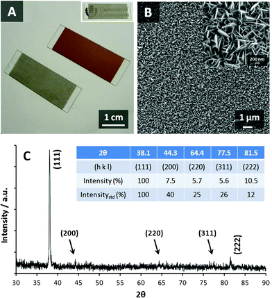 |
| | Fig. 1 (A) Digital image of the metal-coated glass slides before (golden) and after (silvery) the galvanic replacement reaction. (B) FESEM image of Ag thin film with different magnifications. (C) XRD pattern of Ag thin film. Inset of (C): the comparison between the peak intensity of standard FCC Ag and that of the as-prepared sample. | |
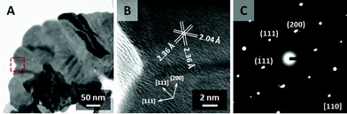
The structural and crystallographic information of the Ag nanopetal was further investigated by transmission electron microscopy (TEM). Fig. 2A gives a bright-field TEM image of a single Ag nanopetal with a height of 200 nm and a length of 400 nm. The highlighted area within the red square was closely examined by high-resolution TEM (HRTEM) and selected area electron diffraction (SAED) along the [110] zone axis. As exhibited in Fig. 2B, the Ag nanopetal is mostly bounded by Ag (111) facet with a d-spacing of 0.236 nm, which is in agreement with the XRD result. Ag (200) facet is also observed with a d-spacing of 0.204 nm. Fig. 2C shows a typical SAED pattern of single crystalline Ag with high lattice perfection, and suggests the anisotropic growth of the nanopetal along [111] direction.
Growth mechanism of Ag nanopetals
The schematic illustration for the formation of Ag nanopetals is presented in Fig. 3. The galvanic replacement reaction initiates at structural defects on the thermal evaporated copper layer, such as intrinsic vacancies and grain boundaries (Fig. S3, ESI†), due to their higher reactivity and better accessibility. Herein, AgNO3 may perform dual functions in the overall reaction process: oxidizing agent as well as etching agent. On one hand, Ag cations gain electrons from Cu atoms and convert to Ag atoms. On the other hand, the weak acidity of the AgNO3 solution slowly etches the surface Cu atoms, generating more structural defects that, in turn, facilitate the subsequent galvanic replacement reaction. The resultant Ag atoms preferentially adopt the (111) plane which is the naturally most stable facet in FCC Ag.23,24 It is worth noting that one Cu atom is substituted by two Ag atoms. Besides, the size of the Cu atom is smaller than that of a Ag atom. Accordingly, the newly produced Ag atoms accumulate favorably along the less crowded, vertical direction instead of the horizontal direction, thus resulting in vertically aligned Ag nanopetals.
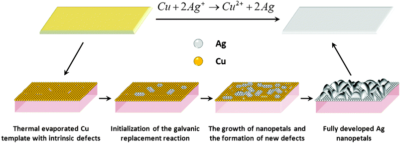 |
| | Fig. 3 Schematic illustration of the growth mechanism of Ag nanopetals from thermal evaporated Cu template. | |
Ag nanopetals in the application of SERS
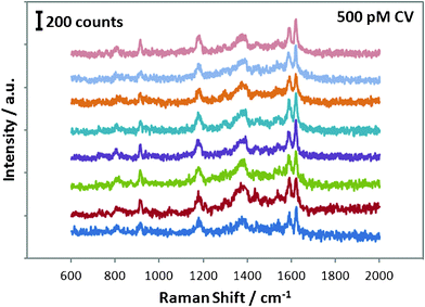
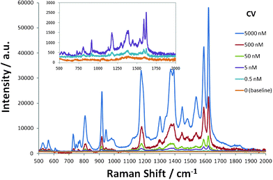
The as-prepared Ag thin film was further explored as a novel SERS substrate in the detection of CV. Fig. 4 shows the Raman spectra of CV with different concentrations on the Ag thin film. The assignments of strong bands at the frequencies (cm−1) of 1620, 1589, 1388, 1177, 915, and 807 are listed in Table 1 according to literature.25,26 A well-resolved SERS spectrum at the concentration of CV as low as 500 pM can still be prominently observed. A modified Freundlich equation,  , which is the most widely used adsorption model for rough surfaces, was utilized to correlate the peak intensity (I) with the concentration of CV (C),27 and the results of a and b along with the value of R2 at different Raman frequencies are shown in Fig. S4† and summarized in Table 1. I0 here is the intensity for the band of interest at the CV concentration of 5 μM. The small standard deviation of the fitting parameters (2.3% for a and 3.7% for b) indicates the analogous influence of CV concentration on all vibrational modes, which indirectly validates the reproducibility of the signal taking into account the fact that the Raman spectrum for each CV concentration was measured inevitably on different spots of the substrate. The results also indicate that the enhancement mechanism might be mainly attributed to the electromagnetic effect instead of chemical effect.27 As shown in Fig. 5, Raman spectra for 500 pM CV were collected on eight pieces of Ag thin film. All the vibrational bands with similar peak intensity for each measurement were observed, which convincingly validates the reliability of the developed nanostructured substrate in SERS application.
 |
| | Fig. 4
Raman spectra of CV with different concentrations on Ag thin film. Inset: magnified Raman spectra for 5 nM, 0.5 nM, and 0 nM (baseline). | |
Table 1 Band assignment of crystal violet and the corresponding fitting parameters for 
| Raman shift (cm−1) |
Assignment |
a
|
b
|
R
2
|
| 1620 |
Ring C–C stretching |
0.5299 |
−4.3652 |
0.992 |
| 1589 |
Ring C–C stretching |
0.5096 |
−4.1771 |
0.991 |
| 1388 |
N–phenyl stretching |
0.4971 |
−4.2208 |
0.997 |
| 1177 |
Ring C–H bending |
0.5253 |
−4.434 |
0.994 |
| 915 |
Ring skeletal vibration |
0.5092 |
−4.4371 |
0.996 |
| 807 |
Ring C–H bending |
0.519 |
−4.6191 |
0.989 |
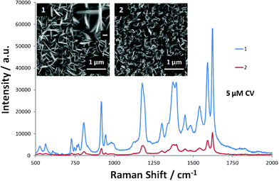
The effect of the density of Ag nanopetals on the Raman signal was also investigated. As shown in Fig. 6, the Raman intensity for 5 μM CV from the Ag nanopetal substrate with lower density is much smaller than that from the one with higher density. Thereupon, the superior enhancement of Raman signal and ultra-sensitivity to analyte can be ascribed to the nanopetal-bounded nanocavities on the developed SERS substrate. Compact Ag nanopetals not only augment the overall surface area but, more importantly, also lead to the formation of nanocavity architecture (inset (1) of Fig. 6). “Hot spots” associated with proximate nanostructures are well-understood in enhancing Raman signal. In addition, nanocavities have also been demonstrated theoretically and experimentally in the enhancement of Raman signal.28 These nanocavities surrounded by vertical Ag nanopetals laterally confine the surface plasmons in a very small volume which can efficiently couple to the incident laser.29 In addition, the electromagnetic energy density inside the nanocavity is greatly enhanced due to the overlap of electric fields resulting from negative curvature.30 All these features contribute to the greatly enhanced Raman signal.
 |
| | Fig. 6
Raman spectra of 5 μM CV on Ag thin films with higher (1) and lower (2) density nanopetals. Inset in (1): one magnified nanocavity with the scale bar representing 100 nm. | |
Calculation of enhancement factor
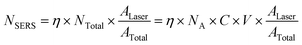
EF is an important parameter to quantify the amplification of SERS for a particular analyte on a given substrate. Therefore, it is an intrinsic property of a specific system, independent of the concentration of the model compound. A comprehensive study of EF has been carried out by Le Ruet al.31EF can be defined as:| | 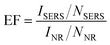 | (1) |
where ISERS is the intensity of the surface-enhanced Raman signal; NSERS is the number of molecules contributing to ISERS; INR is the intensity from the normal Raman signal at the same frequency (as ISERS) on a non-enhanced substrate, such as glass or silicon; NNR is the number of molecules contributing to INR. The values for these parameters were rationalized as follows.
First, ISERS is straightforward to ascertain. On the basis of the discussion above:
| |  | (2) |
In this study, the
ISERS from a lower concentration of the analyte was used in order to minimize the interference from the non-enhanced Raman signal. Therefore, the band at 1177 cm
−1 at the CV concentration of 500 pM is applied, thus
ISERS is 221.2.
Second, the determination of NSERS involves the most difficulty and ambiguity. Herein, we simplify the calculation by defining an adsorption factor (η) which indicates the percentage of molecules absorbed on the surface of the substrate.
| |  | (3) |
NA is the Avogadro constant;
V is the total volume (10 μL) of solution added onto the substrate;
ALaser is the area of laser spot;
ATotal is the total area of the substrate. At the low CV concentration of 500 pM, it is conservative to assume that 15% of molecules are adsorbed on the surface and equally contribute to
ISERS within
ALaser (∼9
CV molecules adsorbed on the probed surface by laser beam).
32,33 Therefore, in our case:
| | 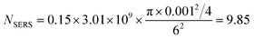 | (4) |
Third, silicon (Si) wafer was applied as the non-enhanced substrate in the measurement of
INR at the CV concentration of 5 mM (Fig. S5, ESI
†). Besides all the vibrational modes of
CV, the strong peak at 520 cm
−1 is the characteristic band of Si, which implies the contribution to the Raman signal from all the molecules added on the substrate. In general, a higher concentration of
analyte (5 mM) is used in order to obtain an explicit Raman spectrum for the determination of
INR. Herein,
INR = 148.7 at 1177 cm
−1.
Finally, NNR can be calculated as follows:
| | 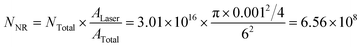 | (5) |
Therefore, according to the definition equation for EF, the enhancement factor of the as-prepared Ag thin film is calculated to be 108. Such a high EF is based on the assumption of 15% (η) of molecules adsorbed on the surface. However, according to literature reports, there is a great possibility for η to be smaller than 15% in the real case which could result in an even larger EF.32,33 In addition, it has been reported that EFs as low as 107 are sufficient for the detection of SERS signals from single molecules.31 By considering the fact that the Raman signal from 9 CV molecules in the probed surface are still obvious in our study, one could expect the detection of a single molecule using the as-prepared Ag nanopetals.
Conclusions
In summary, a transparent Ag thin film was fabricated by a facile, scalable, and economical galvanic replacement reaction method using a Cu-coated glass slide as the template. The uniform distribution of the vertically aligned Ag nanopetals was observed under FESEM, while the highly uniform orientation of the Ag thin film was confirmed by XRD. (HR)TEM and SAED revealed the single crystallinity of the Ag nanopetal which grows preferentially along the [111] direction. AgNO3 plays a pivotal role in the formation of such novel architecture, presumably serving as both oxidizing agent and etching agent. The as-prepared Ag thin film was further applied as a SERS substrate in the detection of CV from 5 μM to 500 pM. The Raman peak intensity and CV concentration can be correlated by the Freundlich equation. ∼9 molecules was estimated to contribute to the Raman signal at the CV concentration of 500 pM, which could result in an EF as large as 108. The outstanding EF was attributed to the “hot spots” resulting from proximate edges of Ag nanopetals and the nanocavities bounded by Ag nanopetals. The excellent reproducibility of the SERS performance was demonstrated by collecting Raman spectra for 500 pM CV on 8 different pieces of Ag thin film. All these features indicate the possibility of detecting single molecules using the as-prepared, cost-effective solid-state SERS substrate.
Acknowledgements
We greatly appreciate the funding from UConn Large Faculty Research Grant and National Science Foundation. LS also thanks the support from the UConn CESE through the Graduate Student Research Assistantship Program in Support of Multidisciplinary Environmental Activities by Faculty Members.
References
- C. L. Haynes, A. D. McFarland and R. P. Van Duyne, Anal. Chem., 2005, 77, 338 A CAS.
- M. G. Albrecht and J. A. Creighton, J. Am. Chem. Soc., 1977, 99, 5215 CrossRef CAS.
- D. L. Jeanmaire and R. P. Van Duyne, J. Electroanal. Chem., 1977, 84, 1 CrossRef CAS.
- M. D. Porter, R. J. Lipert, L. M. Siperko, G. Wang and R. Narayanan, Chem. Soc. Rev., 2008, 37, 1001 RSC.
- S. M. Nie and S. R. Emory, Science, 1997, 275, 1102 CrossRef CAS.
- K. Kneipp, Y. Wang, H. Kneipp, L. T. Perelman, I. Itzkan, R. Dasari and M. S. Feld, Phys. Rev. Lett., 1997, 78, 1667 CrossRef CAS.
- P. L. Stiles, J. A. Dieringer, N. C. Shah and R. R. Van Duyne, Annu. Rev. Anal. Chem., 2008, 1, 601 Search PubMed.
- Y. Fang, N. H. Seong and D. D. Dlott, Science, 2008, 321, 388 CrossRef CAS.
- D. J. Maxwell, S. R. Emory and S. M. Nie, Chem. Mater., 2001, 13, 1082 CrossRef CAS.
- A. Tao, P. Sinsermsuksakul and P. D. Yang, Angew. Chem., Int. Ed., 2006, 45, 4597 CrossRef CAS.
- J. M. McLellan, Z. Y. Li, A. R. Siekkinen and Y. N. Xia, Nano Lett., 2007, 7, 1013 CrossRef CAS.
- K. Ikeda, S. Suzuki and K. Uosaki, Nano Lett., 2011, 11, 1716 Search PubMed.
- J. B. Jackson and N. J. Halas, Proc. Natl. Acad. Sci. U. S. A., 2004, 101, 17930 CrossRef CAS.
- J. P. Camden, J. A. Dieringer, Y. M. Wang, D. J. Masiello, L. D. Marks, G. C. Schatz and R. P. Van Duyne, J. Am. Chem. Soc., 2008, 130, 12616 CrossRef CAS.
- H. H. Wang, C. Y. Liu, S. B. Wu, N. W. Liu, C. Y. Peng, T. H. Chan, C. F. Hsu, J. K. Wang and Y. L. Wang, Adv. Mater., 2006, 18, 491 CrossRef CAS.
- Y. Sawai, B. Takimoto, H. Nabika, K. Ajito and K. Murakoshi, J. Am. Chem. Soc., 2007, 129, 1658 CrossRef CAS.
- Q. M. Yu, P. Guan, D. Qin, G. Golden and P. M. Wallace, Nano Lett., 2008, 8, 1923 CrossRef CAS.
- N. A. Hatab, C. H. Hsueh, A. L. Gaddis, S. T. Retterer, J. H. Li, G. Eres, Z. Y. Zhang and B. H. Gu, Nano Lett., 2010, 10, 4952 CrossRef CAS.
- M. E. Stewart, C. R. Anderton, L. B. Thompson, J. Maria, S. K. Gray, J. A. Rogers and R. G. Nuzzo, Chem. Rev., 2008, 108, 494 CrossRef CAS.
- C. L. Haynes and R. P. Van Duyne, J. Phys. Chem. B, 2003, 107, 7426 CrossRef CAS.
- J. Prikulis, P. Hanarp, L. Olofsson, D. Sutherland and M. Kall, Nano Lett., 2004, 4, 1003 Search PubMed.
- Y. N. Xia and G. M. Whitesides, Angew. Chem., Int. Ed., 1998, 37, 551 CrossRef CAS.
- L. Vitos, A. V. Ruban, H. L. Skriver and J. Kollar, Surf. Sci., 1998, 411, 186 CrossRef CAS.
- Y. G. Sun and Y. N. Xia, Science, 2002, 298, 2176 CrossRef CAS.
- E. N. Esenturk and A. R. H. Walker, J. Raman Spectrosc., 2009, 40, 86 CrossRef CAS.
- M.V. Canamares, C. Chenal, R. L. Birke and J. R. Lombardi, J. Phys. Chem. C, 2008, 112, 20295 CrossRef.
- M. Sackmann, S. Bom, T. Balster and A. Materny, J. Raman Spectrosc., 2007, 38, 277 CrossRef CAS.
- W. F. Hu and S. L. Zou, J. Phys. Chem. C, 2011, 115, 4523 Search PubMed.
- S. Coyle, M. C. Netti, J. J. Baumberg, M. A. Ghanem, P. R. Birkin, P. N. Bartlett and D. M. Whittaker, Phys. Rev. Lett., 2001, 87, 1768011 Search PubMed.
- Q. Zhou, H. Zhao, F. Z. Pang, Q. Y. Jing, Y. Wu and J. W. Zheng, J. Phys. Chem. C, 2007, 111, 514 CrossRef CAS.
- E. C. Le Ru, E. Blackie, M. Meyer and P. G. Etchegoin, J. Phys. Chem. C, 2007, 111, 13794 CrossRef CAS.
- Y. Wang, M. Becker, L. Wang, J. Q. Liu, R. Scholz, J. Peng, U. Gosele, S. Christiansen, D. H. Kim and M. Steinhart, Nano Lett., 2009, 9, 2384 CrossRef CAS.
- J. X. Fang, S. Y. Liu and Z. Y. Li, Biomaterials, 2011, 32, 4877 CrossRef CAS.
Footnote |
| † Electronic supplementary information (ESI) available: EDXS, additional FESEM images, derivation of a, b, and R2 in Table 1, and the Raman spectrum of INR. See DOI: 10.1039/c1ra00827g |
|
| This journal is © The Royal Society of Chemistry 2012 |
Click here to see how this site uses Cookies. View our privacy policy here.