The electroless nickel plating of catalytically graphitized electrospun carbon nanofibers
Ali Mohammad
Bazargan
*,
Sasan
Ghashghai
,
Mansour
Keyanpour-rad
and
Maryam
Esmaeilpour Ganji
Materials and Energy Research Center, P. O. Box 14155-4777, Tehran, Iran. E-mail: ambazargan@merc.ac.ir; Fax: +98-2188773352; Tel: +98-9131147323
First published on 4th January 2012
Abstract
Catalytically graphitized electrospun carbon nanofibers were plated with nickel using a commercial electroless bath for the first time. The nanofiber fabrication process was performed in the presence of nickel as the graphitization catalyst at a temperature of 1400 °C. Raman spectroscopy and X-ray diffraction studies confirmed the achievement of a satisfactory degree of graphitization for the carbon nanofibers. After sensitization and activation processes, the nanofibers were submerged for 20 min in the electroless bath at a temperature of 45 °C and a pH value of 9. Results from scanning electron microscopy and X-ray diffraction showed that a pure, crystalline and uniform nickel coating of 186 nm thickness was formed on the surface of the nanofibers.
Introduction
One dimensional carbon nanostructures have different properties that make them suitable candidates for diverse applications. As a whole, their high thermal and chemical stability, proper strength and specific module accompanied by low mass density and variety of electrical behaviors are qualities which conform to purposes like composite construction, nanoelectronics, hydrogen storage, nanosensors etc.1,2 1D carbon nanostructures can be found in different shapes, for example as whiskers, nanotubes or nanofibers. Carbon nanofibers (CNFs) are commonly in the diameter range of 50–200 nm and are to some extent similar to multiwalled nanotubes, regardless of having dissimilar types of standing graphite layers. The CNFs are generally produced in the temperature range of 400–1100 °C by catalytic decomposition of hydrocarbon gases like CO on metal particles such as Fe, Ni, Co and some of their alloys. The two most practical techniques are chemical vapor deposition (CVD) and catalytic chemical vapor deposition (CCVD).3Electrospinning is almost a new process in the CNFs' world which is based on the electrostatic deposition of fibers from a polymer solution.4,5 This technique has unique attributes, such as ease of production, repetition capability and potential to produce long continuous nanofibers which make it a reasonable process for industrial applications.
Producing CNF-reinforced composites, as commercial and military components used in the aviation industry, is one of the attractive fields for scientists owing to their light weight and high thermal conductivity. Nowadays Al–matrix composites are regarded as the most applicable composites in automotive, aviation and defence industries due to their high specific strength. So CF/Al composites have specific qualities compared to other composites which increase their application potential in the aeronautics industry.
In general, fiber-reinforced metal–matrix composites have unique advantages like high strength, high specific module, considerable electrical and thermal conductivity and low thermal expansion. Applying the CNFs in a metallic matrix faces two important challenges, however. The first crisis is related to the reactive tendency of Al and carbon fibers which depends on the thermodynamic and kinetic circumstances. The undesirable outcome of this reaction, Al4C3 formation, brings about weak mechanical properties especially at their interface. The other problem is low wettability of CNFs by the metal matrix caused by electrostatic repulsion of charges.6,7 Since CNFs are new member of fibrous reinforcements with superior advantages compared to microfibers, it is necessary to find a solution to conquer these difficulties. Both of these problems can be overcome by applying a proper coating over fibers or chemical modification of the matrix. Ni coating is an optimal solution to prevent the formation of Al4C3. One of the useful techniques to apply a nickel-coating on carbon fibers is electroless plating. Compared to other coating methods, electroless plating is more practical because of its low cost, high throwing power, ability of coating conductive and semiconductive surfaces, and ability to apply continuous and uniform coatings with high hardness and corrosion resistance. Arai et al. used an electroless deposition process and homogeneously coated the commercial vapor-grown carbon nanofibers (VGCFs) with nickel.8
It is well established that the electroless nickel coatings deposited using sodium hypophosphite as a reducing agent are binary alloys of nickel and phosphorus. The phosphorus content, which could be controlled by varying the deposition parameters, such as pH value, bath composition, etc., plays an important role in the structure and properties of the coatings.9
This article is the first reported study on nickel coating of catalytically graphitized electrospun carbon nanofibers (CGECNFs) using the electroless technique. The process parameters were precisely controlled so that the best possible purity, crystallinity and uniformity were achieved for the Ni coating. The coating was then subjected to different analyses to evaluate its morphology and microstructure. The results revealed the high quality of the Ni layer over the nanofibers.
Experimental
Preparation of CGECNFs
A 12wt% polyacrylonitrile (PAN, Mw = 80 kg mol−1, Isfahan Polyacryle Co.) solution including DMF (Merck) supplemented with Ni(acac)2 in the proportion of 1![[thin space (1/6-em)]](https://www.rsc.org/images/entities/char_2009.gif) :5 to PAN was treated by 24-hour stirring at room temperature. The purpose of utilizing Ni(acac)2 was having a source of Ni catalyst as a stimulant to graphitize CNFs. The as prepared solution was subsequently electrospun with a constant feed rate of 0.5 cm3 h−1 at a positive voltage of 11.5 kV and a collection distance of 10 cm with the aid of the electrospinning setup used in our previous studies.10,11 The electrospun nanofibers afterwards were stabilized in a tubular furnace for 1 h at 230 °C in air. The fibers were then heated at a rate of 3 °C min−1 under a N2 atmosphere and were maintained at 800 °C for 1 h, followed by 1400 °C for a period of 2 h.
:5 to PAN was treated by 24-hour stirring at room temperature. The purpose of utilizing Ni(acac)2 was having a source of Ni catalyst as a stimulant to graphitize CNFs. The as prepared solution was subsequently electrospun with a constant feed rate of 0.5 cm3 h−1 at a positive voltage of 11.5 kV and a collection distance of 10 cm with the aid of the electrospinning setup used in our previous studies.10,11 The electrospun nanofibers afterwards were stabilized in a tubular furnace for 1 h at 230 °C in air. The fibers were then heated at a rate of 3 °C min−1 under a N2 atmosphere and were maintained at 800 °C for 1 h, followed by 1400 °C for a period of 2 h.
Nickel electroless plating
After structural and morphological investigations on the heat treated nanofibers, the sample was coated in a 9-pH commercial Ni electroless bath for 20 min. Prior to the coating process, sensitization and activation were used for catalyzing the CNFs. The sensitizer and activator were stannous chloride/hydrochloric acid (6 g L−1 SnCl2·2H2O and 20 ml L−1HCl) and palladium chloride/hydrochloric acid (0.1 g L−1PdCl2 and 1.2 ml L−1HCl) solutions, respectively. Magnetic stirring was applied during the catalyzing treatment to facilitate uniform activation throughout the entire surface of the CNFs. Both previous steps made preferential sites of Sn2+ and Pd2+ ions on the fibers to arrange the reduction reaction and hence Ni deposition. The solution then passed through a strainer and resulting nanofibers were placed in a 45 °C electroless bath for 20 min under continuous stirring. Because of stirring, the precursors have the possibility of touching the fibers continuously which enhances the diffusion mechanism. As a result, the reduction reaction will be accelerated. After coating, the CGECNFs containing solution was filtered and the obtained fibers were dried for 1 h in an oven at 80 °C. Then the coated CGECNFs were conclusively scrutinized in order to study their morphological and structural properties.Characterizations
The surface morphology of CGECNFs was observed by a scanning electron microscope (SEM-S360 Cambridge) working at 20 kV of accelerating voltage. Before observation, the samples were coated with a thin layer of gold to avoid the problem of charge effect. The average diameter of the fibers before and after coating was appraised from the SEM images in the original magnification of 10 k, using ImageJ software.10–12 Toward identifying the formed phases, X-ray diffraction (XRD) patterns were obtained using a Philips X-ray diffractometer (PW3710) with graphite-monochromatized high intensity Cu-Kα radiation (λ = 1.540598 Å) operated at 30 kV and 25 mA within the range of 2θ = 20–80°, with a step size of 0.02° and time per step of 100 s. The mean interlayer spacing, d002, was determined from the position of the (0 0 2) peak applying Bragg's equation. The mean crystallite size, Lc was calculated from the (0 0 2) peak width using the Scherrer formula with K = 0.9.13The Raman spectrum was recorded using an Almega Raman Spectrometer with a 514.5 nm He–Ne laser line as the excitation source in the range of 1000–1700 cm−1.
Results and discussion
SEM images of CGECNFs at different magnifications are shown in Fig. 1. As can be seen in Fig. 1a, numerous thin and smooth nanofibers with large area uniformity and desired morphology have been attained. Image processing studies indicated an almost narrow range of variation for graphitized nanofibers' diameter and estimated an average fiber diameter of 162 ± 22 nm. A small number of dispersed nanoparticles in the diameter range of 40–60 nm are also observed on the graphitized nanofibers (Fig. 1c) which seem likely to be nickel nanoparticles as the product of the Ni(acac)2 decomposition reaction. The relatively low concentration of the nickel nanoparticles might be attributed to the small proportion of nickel salt precursor in the solution.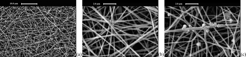 | ||
| Fig. 1 SEM images of CGECNFs (a) at 2.5 K× and (b) 10 K×, (c) SEM image of nickel nanoparticles grown on CGECNFs. | ||
It has been shown that addition of certain inorganic and organic additives enhances the graphitization process with lower temperature needed to bring about a certain degree of graphitization. This phenomenon is called catalytic graphitization and nickel has been known to be one of the most efficient catalysts for the graphitization of amorphous carbons.14
With the purpose of attaining graphitized electrospun nanofibers in an inert atmosphere, the Ni(acac)2 was added to the electrospinning solution and a high temperature heat treatment was carried out on the nanofibers. It was anticipated that during the heat treatment, the Ni(acac)2 decomposes into the corresponding nickel catalyst and a higher graphitization degree can be achieved.
Fig. 2 displays the XRD pattern of the CGECNF sample after heat treatment. At 1400 °C, the obtained data for the sample has a marked sharp reflection peak at approximately 2θ = 26.08° corresponding to the diffraction of the (0 0 2) plane of the graphite structure with a mean interlayer spacing, d002, of 0.3415 nm and mean crystallite size, Lc, of 6.41 nm (see Table 1) which are very close to the values reported before.17,18 In the XRD scan, the diffraction peak at 2θ = 44.4° corresponding to Ni (111) can also be clearly seen. It is recognized that Ni(acac)2 dissolved in the precursor solution was converted into Ni throughout carbonization, as was supposed earlier, which could provoke the graphitization reaction. In electrospun CNFs, the existence of micropores discussed in our previous work10,11,16 demonstrates a good motivation to enhance mass transfer and therefore the interactions between the deposited Ni catalytic phase and its support, leading to the formation of CGECNFs.
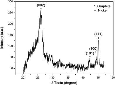 | ||
| Fig. 2 XRD pattern of CGECNFs. | ||
For the PAN-based graphitized nanofibers, the crystalline structure of graphite was well characterized by Raman spectroscopy and the result is represented in Fig. 3. The hexagonal crystal graphite structure shows a Raman active peak at 1576 cm−1 (G mode), and the band around 1342 cm−1 can be attributed to the D mode of disorder-induced scattering, which is due to imperfections or lack of hexagonal symmetry in the carbon structure.17Table 1 reveals the relative intensity (ID/IG) of the structure in the Raman spectrum which reflects the crystallite planar size of the graphite.
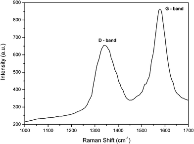 | ||
| Fig. 3 Raman spectrum of CGECNFs. | ||
The ratio of the G-band versus the D-band presents a satisfactory degree of graphitization of the as-synthesized CGECNFs which had been illustrated by the XRD results too. As shown in Table 1, the obtained relative intensity (ID/IG) equals to 0.76 which is very close to the relative intensity reported before even at higher performance temperature (1500 °C).15
After the electroless plating process, the morphological properties of the sample were investigated again. The related SEM examination, shown in Fig. 4a, confirms that by using the electroless bath for 20 min, graphitized electrospun nanofibers have been coated homogeneously along their length. Using image processing techniques, it was determined that the Ni-coated electrospun CNFs have an average diameter of 348 ± 30 nm and the thickness of the deposited Ni coating is 186 nm.
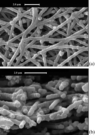 | ||
| Fig. 4 SEM images of (a) surface and (b) cross section of Ni-coated CGECNFs. | ||
Since it is important to provide an intact coating over the fibers in order to prevent the formation of brittle phases in the carbon fiber-reinforced composites,15 the cross section of coated nanofibers was also observed under SEM (Fig. 4b). As the figure reveals, the Ni coating thickness has been accurately controlled thanks to the perfect diffusion of solution through the triple process of coating that has been supplied by a combination of electrospinning/electroless plating methods. The SEM results also prove that the stability and activity of the highly porous CGECNF support along with desired textural and surface properties provides good conditions for Ni coating deposition.
The XRD pattern of Ni-coated CGECNFs is shown in Fig. 5. The intense diffraction peak at around 2θ = 45° is attributed to the (111) plane of Ni which has dramatically increased compared with the corresponding peak in Fig. 2, as a consequence of the formation of pure crystalline FCC Ni coating over the CGECNFs.
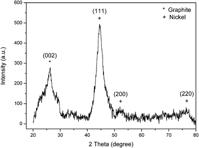 | ||
| Fig. 5 XRD pattern of Ni-coated CGECNFs. | ||
Conclusions
A pure, crystalline and uniform nickel coating of 186 nm thickness was successfully applied on the entire surface of CGECNFs by an electroless plating method for the first time. To achieve this goal, the electrospun CNFs were catalytically graphitized in the presence of nickel at a temperature of 1400 °C. Raman spectroscopy and XRD analyses confirmed the achievement of a satisfactory degree of graphitization for the electrospun CNFs. After being sensitized and activated, the CNFs were submerged for 20 min in a nickel electroless bath at a temperature of 45 °C and a pH value of 9. The SEM and XRD analyses were used to investigate the morphological and structural properties of the Ni coating as well as the CNFs.References
-
J. B. Donnet, R. C. Bansal and M. J. Wang, Carbon Fibers, 3rd edn, Dekker, New York, 1990 Search PubMed
.
- S. J. Park and M. S. Cho, Carbon, 2000, 38, 1053 CrossRef CAS
- S. Chand, J. Mater. Sci., 2000, 35, 1303 CrossRef CAS
- F. Ko, Y. Gogotsi, A. Ali and N. Naguib, Adv. Mater., 2003, 15, 1161 CrossRef CAS
- Y. Wang, S. Serrano and J. J. Santiago-Aviles, Synth. Met., 2003, 138, 423 CrossRef CAS
- S. Subramanian, J. Reinforc. Plast. Compos., 1997, 16, 676 CAS
- E. Ghorbel, Compos. Sci. Technol., 1997, 57, 1045 CrossRef CAS
- S. Arai, M. Endo, S. Hashizume and Y. Shimojima, Electrochem. Commun., 2004, 6, 1029 CrossRef CAS
- S. Tzeng and F. Chang, Thin Solid Films, 2001, 388, 143 CrossRef CAS
- A. M. Bazargan, S. M. A. Fateminia, M. Esmaeilpour Ganji and M. A. Bahrevar, Chem. Eng. J., 2009, 155, 523 CrossRef CAS
- M. Esmaeilpour Ganji, A. M. Bazargan, M. Keyanpour-rad and M. A. Bahrevar, Funct. Mater. Lett., 2010, 3, 141 CrossRef
- A. M. Bazargan, M. Naghavi, M. Mazaheri and S. K. Sadrnezhaad, Ceram. Int., 2009, 35, 1139 CrossRef CAS
- J. Biscoe and B. J. Warren, J. Appl. Phys., 1942, 13, 364 CrossRef CAS
- F. Zhang, D. He, S. Ge and Q. Cai, Surf. Coat. Technol., 2008, 203, 99 CrossRef CAS
- M. Weisenberger, I. Martin-Gullon, J. Vera-Agullo, H. Varela-Rizo, C. Merino and R. Andrews,
et al.
, Carbon, 2009, 47, 2211 CrossRef CAS
- A. M. Bazargan, M. Keyanpour-rad, F. A. Hesari and M. Esmaeilpour Ganji, Desalination, 2011, 265, 148 CrossRef CAS
- I. S. Kim and S. K. Lee, Scr. Mater., 2005, 52, 1045 CrossRef CAS
- A. Berner, K. C. Mundim, D. E. Ellis, S. Dorfman, D. Fuks and R. Evenhaim, Sens. Actuators, A, 1999, 74, 86 CrossRef
| This journal is © The Royal Society of Chemistry 2012 |