On-chip diameter-dependent conversion of metallic to semiconducting single-walled carbon nanotubes by immersion in 2-ethylanthraquinone
Jiangbo
Li
a,
Xuena
Luan
a,
Yinxi
Huang
a,
Simon
Dunham
b,
Peng
Chen
*a,
John A.
Rogers
*b and
Mary B.
Chan-Park
*a
aSchool of Chemical & Biomedical Engineering, Nanyang Technological University, 62 Nanyang Drive, Singapore 637459, Singapore. E-mail: mbechan@ntu.edu.sg; Chenpeng@ntu.edu.sg
bDepartment of Materials Science and Engineering, Beckman Institute, and Frederick Seitz Materials Research Laboratory, University of Illinois at Urbana-Champaign, 1304 West Green Street, Urbana, Illinois 61801, USA. E-mail: jrogers@illinois.edu
First published on 22nd December 2011
Abstract
The key hurdle to the practical use of as-grown single-walled carbon nanotubes (SWNTs) for high performance nanoelectronics is the unavoidable presence of metallic nanotubes with current synthesis methods. We present a simple approach to convert metallic SWNTs to semiconducting ones in situ to improve device field effect behaviour, using an aromatic compound (2-ethylanthraquinone - EAQ) which is a mild radical initiator. We show that the reaction between EAQ-generated radicals and SWNTs is diameter and metallicity dependent; in the medium-diameter regime (0.8 to 1.0 nm), the EAQ-generated radicals preferentially attack the metallic SWNTs over semiconducting ones and convert them to semiconducting, as evidenced by several orders (10 and 104) increase in the on/off ratio.
Single-walled carbon nanotubes (SWNTs) have attracted great interest due to their extraordinary electrical properties1 and their promising applications in future electronics have been extensively explored.2–5 In particular, compared with current Si-based devices, SWNT-based field-effect transistors (SWNT-FETs) show unique advantages.6 Despite significant progress being made toward SWNT-based circuits,7–9 there are still obstacles for exploiting their full potential in real application. A central issue for obtaining superior FET devices is to minimize the presence or influence of metallic SWNTs (M-SWNTs) in the active channels.
To tackle this issue, various approaches have been developed, including solution-based pre-sorting or pre-separation of the two types of nanotubes,10–11 selective synthesis of semiconducting SWNTs (S-SWNTs),12–13 selective chemical modifications,14–16 electrical breakdown of M-SWNTs,17 or selective etching of M-SWNTs by methane plasma18 and light irradiation.19–20 An appealing alternative is to convert M-SWNTs into S-SWNTs in situ, which has been realized using electron irradiation21 and hydrogen plasma.22–23 Recently, the transition of SWNT from metallic to semiconducting was also achieved through helical wrapping of DNA.24 However, electron irradiation is highly difficult to scale up due to limited size of electron beam. Hydrogen plasma is aggressive and cannot be controlled precisely.
Here, we demonstrate the use of 2-ethylanthraquinone (EAQ) (Fig. 1a) to fulfil the on-chip metal-to-semiconductor transition of individual as-grown SWNTs for application in field effect transistors. This approach is simple, mild and easily scalable to whole wafers (illustrated in Fig. 1b). Fig. 1c shows the transfer characteristics (drain current Idsversus gate voltage Vg) for a typical device, with a single metallic SWNT as the conducting channel, before and after 7-day EAQ treatment. The scanning electron microscopy (SEM) of the device is also shown in Fig. 1c inset. We observed a considerable increase in the channel current on/off ratio (Ion/Ioff) from ∼1.47 to ∼1.63 × 10³ after EAQ treatment. The increase of on/off ratio implies the conversion from M-SWNTs to S-SWNTs.
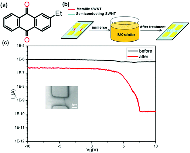 | ||
| Fig. 1 (a) Structure of 2-ethylanthraquinone (EAQ). (b) Schematic illustration of the treatment process for SWNT-FET in the EAQ solution. (c) Transfer characteristics (Vds = 0.5 V) of a single metallic SWNT-FETs before (black) and after (red) EAQ treatment. The on/off ratio increased from ∼1.47 to ∼1.63 × 10³. Inset is SEM image of the SWNT-FET. | ||
Here, we applied electrical measurements and Raman characterizations to investigate the effect of EAQ treatment to SWNTs in the channel of FET devices. With SWNTs, the Raman spectroscopy25–29 can detect the distinct vibration modes and their defects by G and D bands, respectively. Fig. 2a and 2b show the Raman spectra and Ids-Vg curves of a single metallic nanotube device before and after EAQ treatment. The Raman spectra reveals an increase in the D band intensity (1329.6 cm−1) and a decrease in the G band intensity (1592.4 cm−1), accompanied by a G band upshift of 3.5 cm−1. There is a 4-fold decrease in the ratio between the G and D band intensities (IG/ID) after EAQ treatment (Fig. 2a), which can be attributed to an increase in the defect density on the SWNT sidewall.22 We suggest that EAQ treatment introduced disorder on the SWNT wall, and thus increased the D band density. The Ids-Vg curve (Fig. 2b) shows a decrease in nanotube's conductance, and a significant increase in the gate-voltage dependence after EAQ treatment. These observations can be attributed to that defects introduced by conversion of sp2 hybridized carbon structure to sp3 structure in SWNT through covalent chemistry should strongly affect Fermi level of metallic tubes, and can result in localization of π-electrons, and consequently, opening up the band gap of SWNT.22,30 The conversion of sp2 to sp3 structure transforms the nature of the nanotube from metallic to semiconducting.30–32
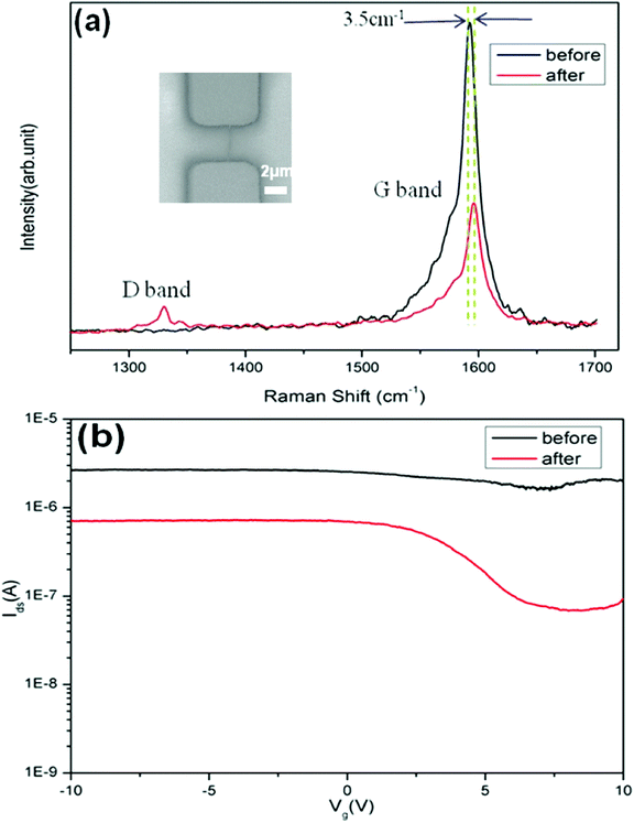 | ||
| Fig. 2 (a) Raman spectra showing D band and G band of a single metallic SWNT in the FET device before (black) and after (red) EAQ treatment. Inset is SEM image of the metallic single-tube device. (b) Current (Ids) versus gate voltage (Vg) characteristics of the device (inset of a) before (black) and after (red) EAQ treatment, showing decrease of the overall conductance and Ion/Ioff improvement from 1.5 to 10.7. The stronger gate bias dependence of device indicated metal-to-semiconductor conversion of SWNT. | ||
We treated 64 as-synthesized single-SWNT devices by immersing them into EAQ solution for seven days. Here, a “Lost” device is the one with Ion < 100 pA at Vds = 0.5 V. The “Lost” devices have very low on/off ratio (Ion/Ioff ≈ 1) since their Ids-Vg curve is flat. “Depletable” (D) devices are defined as having Ion > 1 nA and Ion/Ioff ≥ 10, and “Nondepletable” (ND) devices are those with Ion/Ioff < 10. We observed five different device behaviours after the treatment, including D→Lost (becoming electrically nonconductive (Fig. 3a)), ND→Lost (Fig. 3b), ND→D (nondepletable became depletable) (Fig. 3c), ND→ND (Fig. 3d), and D→D (Fig. 3e).
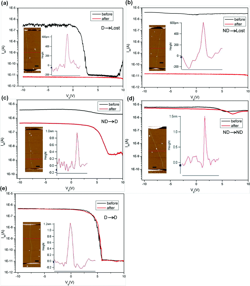 | ||
| Fig. 3 (a to e) Ids-Vg curves (Vds = 0.5 V) showing five different device behaviours before (black) and after (red) EAQ treatment. Insets in each diagram are AFM images of the SWNT in the device channel and surface height plot showing the tube diameter. The scale bars are 500 nm. | ||
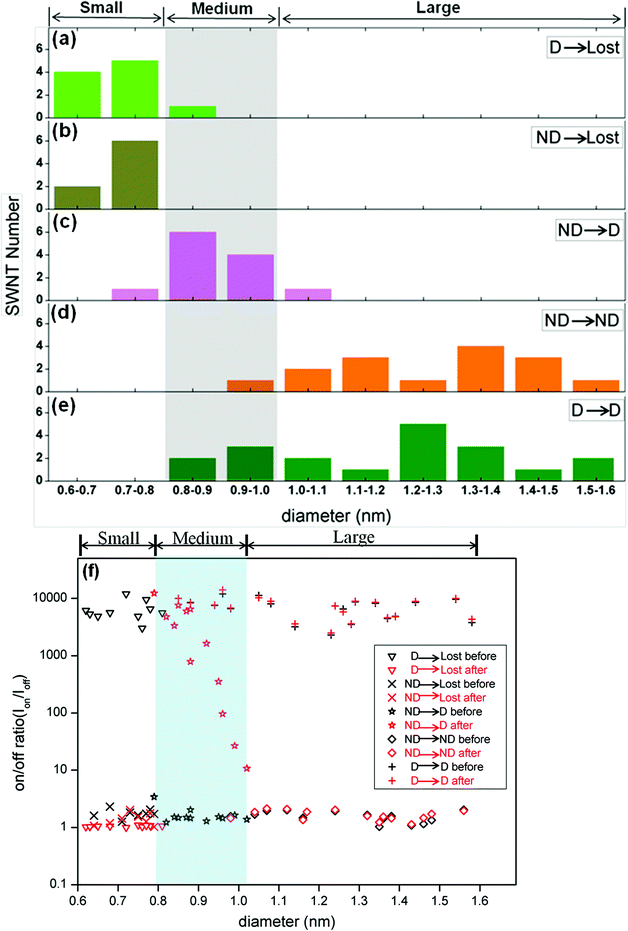 | ||
| Fig. 4 (a to e) Diameter distribution (from AFM measurements) of SWNTs in devices grouped by their behaviour under EAQ treatment. The smaller-diameter (0.60 nm–0.80 nm) SWNTs (a and b), whether metallic or semiconducting, were “Lost” after treatment. In ND→D devices (c), the metallic tubes, mainly in the medium-diameter regime (from 0.80 nm to 1.00 nm), were converted into semiconducting ones by EAQ treatment. Large metallic SWNTs with diameter between 1.00 nm and 1.60 nm in ND devices (d) were only slightly affected by EAQ treatment. D→D devices (e) exhibited a wider diameter distribution spanning medium and large regimes, indicating that semiconducting SWNTs of medium diameter were less reactive than metallic tubes of the same diameters. (f) On/off ratio (Ion/Ioff) versus SWNT diameter before (black) and after (red) EAQ treatment. In the small-diameter range (0.60 nm < d < 0.80 nm), both metallic SWNTs in ND devices and semiconducting SWNTs in D devices lost conductance (ND→Lost and D→Lost). For D→Lost devices, Ion/Ioff decreased a lot. For ND→Lost devices, Ion/Ioff had little change before and after treatment. In the medium-diameter range (0.80 nm < d < 1.00 nm), Ion/Ioff in ND devices with metallic SWNT improved several orders (10 to 104) after EAQ treatment. High Ion/Ioff in D devices with semiconducting SWNT was preserved (D→D). In the large-diameter range (1.00 nm < d < 1.60 nm), Ion/Ioff in both ND and D devices were nearly no change (ND→ND and D→D). | ||
AFM measurements were carried out to obtain the diameters of SWNTs in the channel of devices. No visible etching and change in the SWNTs diameters were observed after EAQ treatment in all AFM images. We found that the D→Lost devices were composed of predominantly small-diameter semiconducting SWNTs (S-SWNTs) with d < 0.80 nm (Fig. 3a inset and 4a). For the ND→Lost devices which are composed of initially metallic nanotubes instead (Fig. 3b), AFM analysis shows that the diameters of these tubes were also relatively small, with a diameter range from 0.6 to 0.8 nm (Fig. 3b inset, Fig. 4b). It is well-accepted that SWNTs with smaller diameters are preferentially reactive over larger ones due to the higher C–C bond strain and radius of curvature of the former tubes.18,33 Our results are in support of this notion. The smaller-diameter SWNTs (0.60 nm < d < 0.80 nm), whether metallic or semiconducting, were nondiscriminatingly overreacted in our studies, and finally losing electrical conductance. For the medium diameter nanotubes (0.8 nm < d < 1.00 nm), the metallic species (Fig. 3c inset) became switchable after the chemical treatment so that devices underwent ND→D change after EAQ treatment, indicating conversion of the nanotubes from metallic to semiconducting. For the ND→ND devices (Fig. 3d), most of the nanotubes had large diameters (d > 1.00 nm, in Fig. 4d). This suggests that large-diameter metallic SWNTs (1.00 nm < d < 1.60 nm) are likely inert to EAQ treatment. On the other hand, in D→D devices, the semiconducting tubes (Fig. 3e inset) were observed to have a wider diameter span from 0.80 nm to 1.60 nm (Fig. 4e) and these devices preserved the gate-voltage dependence after the treatment. In Fig. 4f, the changes of on/off ratio (Ion/Ioff) before (black) and after (red) EAQ treatment can be easily observed. In the small-diameter range (0.60 nm < d < 0.80 nm), both metallic SWNTs in ND devices and semiconducting SWNTs in D devices lost conductance (ND→Lost and D→Lost). For D→Lost devices, Ion/Ioff decreased a lot. For ND→Lost devices, Ion/Ioff had little change before and after treatment since Ion/Ioff of ND devices is nearly 1 and Ion/Ioff of lost devices is also about 1. In the medium-diameter range (0.80 nm < d < 1.00 nm), Ion/Ioff in ND devices with metallic SWNT improved several orders (10 to 104) after EAQ treatment, indicting conversion from metallic to semiconducting ones (ND→D). High Ion/Ioff in D devices with semiconducting SWNT was preserved (D→D), implying semiconducting SWNT was inert to EAQ treatment. In the large-diameter range (1.00 nm < d < 1.60 nm), Ion/Ioff in both ND and D devices were nearly no change (ND→ND and D→D), exhibiting large-diameter SWNTs kept their electronic property.
Taken together, our results suggest that only in the medium-diameter regime (0.80 nm to 1.00 nm), metallic tubes are preferentially reactive over semiconducting ones in EAQ solution (Fig. 4a–4e). In other words, in this regime, the effect of EAQ treatment depends on the electronic properties of nanotubes. In contrast, in the large diameter range (1.00 nm < d < 1.60 nm), both M- and S-SWNTs were nearly unaffected after EAQ treatment. According to first-principle calculations, M-SWNTs have higher formation energy than same-diameter S-SWNTs.34–35 Also, more abundant delocalized electronic states of M-SWNTs result in their higher chemical reactivity.35 The reactivity difference diminishes for SWNTs with large diameters,18,34 consistent with reduced chemical selectivity seen here for large-diameter SWNTs.
The behavior of these EAQ treated devices is relatively stable. The devices after EAQ treatment show similar behavior even after annealing (in Ar, 300 °C, 30 mins). The devices cannot be converted back to metallic after high temperature annealing. This is different from previous studies using dizonium salt.14
According to ab initio calculations, binding energy between EAQ and metallic/semiconducting SWNT is zero, which means, EAQ does not bind to the semiconducting or metallic SWNT.36–37 So when we investigate the mechanism of tube conversion, charge transfer between EAQ and SWNT can be ruled out. It is well-known that EAQ can generate radicals under light.37–38 We attribute the observed metal-to-semiconductor conversion to the attack of light-induced radicals toward the sidewall of M-SWNTs, which alters the carbon lattice structure by covalently adding chemical functionalities, and consequently open up or increase the band gap of M-SWNTs.39–40 Such a reaction process is illustrated in Fig. 5a. In the FTIR spectroscopy (Fig. 5b), increased absorption in the region 3100–3600 cm−1 was observed on CoMoCAT SWNTs samples after EAQ treatment, indicating the abundant existence of oxygenated functionalities in treated SWNTs mainly in the form of hydroxyl groups. Addition of oxygen functionalities to SWNTs' sidewall could withdraw electrons from SWNTs,41–42 resulting in upshift of Raman G band of nanotube as observed in Fig. 2a.43–44
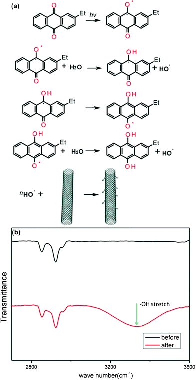 | ||
| Fig. 5 (a) Schematic illustration of the reaction mechanism in the EAQ treatment process. (b) FTIR spectra of SWNTs before (black) and after (red) EAQ treatment. | ||
In summary, this work demonstrates a simple and scalable method to improve the switching of SWNT-based FET devices by in situ conversion of as-grown metallic SWNTs to semiconducting ones using photoinitiated radicals. This approach was found to be diameter dependent and highly effective among SWNTs with medium diameters of 0.80 nm to 1.00 nm, in which regime the density of states near the Fermi level dictates the reactivity of SWNTs, and M-SWNTs with more abundant density of states show preferential reactivity over s-SWNTs. The enhancements of on/off ratio in FET devices after EAQ treatment generally ranged between 10 and 104. Compared to other radical treatment methods, this process is mild. This approach provides a possibility to achieve SWNT-based integrated circuits.
Experimental section
Materials preparation and device fabrication
SWNTs were grown on the silicon wafer with 400 nm oxide layer using CVD method.9,45 Briefly, the catalyst consisted of ferritin (Aldrich; diluted with de-ionized water at a volumetric ratio of 1![[thin space (1/6-em)]](https://www.rsc.org/images/entities/char_2009.gif) :2000) was deposited onto the SiO2–Si surface. The wafer was then heated to 800 °C in a quartz tube to oxidize ferritin into iron oxide nanoparticles. Growth temperature was 925 °C. Ethanol was released into the quartz tube as a carbon source. Growth time was 5 mins. After CVD growth, we used microfabrication techniques to pattern source–drain (S–D) electrode pads to contact SWNTs.18 We chose Ti/Au (10 nm/20 nm) as the contact metal in the current work. The channel length was 5 μm, and the width was 6 μm. 2-Ethylanthraquinone (EAQ) and other chemicals were purchased from Sigma-Aldrich. EAQ (30 mg) was dissolved in a mixture of dimethylformamide (DMF, 25 mL) and DI water (5 mL) by water-bath sonication for 10 mins. SWNT-based devices were immersed in the EAQ/DMF solution. Then the sample was placed in ambient condition (under the light and air) for several days. When finishing, the wafer was taken out of the solution, and washed with DMF, ethanol, and DI water. Then the wafer was dried in the oven overnight to completely remove the solvent. To obtain FTIR signals of detectable amplitude, we used CoMoCAT carbon nanotubes purchased from Southwest Nanotechnologies. CoMoCAT tubes were dispersed in DMF/DI water solution with or without EAQ, respectively. After reaction for 7 days, the solution was filtered through a PTFE membrane (0.2 μm), and rinsed with DMF, ethanol, and DI water. SWNTs solid was transferred to quartz substrates, and dried at 120 °C in the vacuum oven before FTIR characterization.
:2000) was deposited onto the SiO2–Si surface. The wafer was then heated to 800 °C in a quartz tube to oxidize ferritin into iron oxide nanoparticles. Growth temperature was 925 °C. Ethanol was released into the quartz tube as a carbon source. Growth time was 5 mins. After CVD growth, we used microfabrication techniques to pattern source–drain (S–D) electrode pads to contact SWNTs.18 We chose Ti/Au (10 nm/20 nm) as the contact metal in the current work. The channel length was 5 μm, and the width was 6 μm. 2-Ethylanthraquinone (EAQ) and other chemicals were purchased from Sigma-Aldrich. EAQ (30 mg) was dissolved in a mixture of dimethylformamide (DMF, 25 mL) and DI water (5 mL) by water-bath sonication for 10 mins. SWNT-based devices were immersed in the EAQ/DMF solution. Then the sample was placed in ambient condition (under the light and air) for several days. When finishing, the wafer was taken out of the solution, and washed with DMF, ethanol, and DI water. Then the wafer was dried in the oven overnight to completely remove the solvent. To obtain FTIR signals of detectable amplitude, we used CoMoCAT carbon nanotubes purchased from Southwest Nanotechnologies. CoMoCAT tubes were dispersed in DMF/DI water solution with or without EAQ, respectively. After reaction for 7 days, the solution was filtered through a PTFE membrane (0.2 μm), and rinsed with DMF, ethanol, and DI water. SWNTs solid was transferred to quartz substrates, and dried at 120 °C in the vacuum oven before FTIR characterization.
Characterization
Raman spectra of the samples were measured with a Renishaw Ramanscope in the backscattering configuration, and Stokes spectra of the samples were obtained with 633 nm lasers. Atomic force microscopy (AFM) was conducted using a MFP 3D microscope (Asylum Research, Santa Barbara, CA, USA) with a cantilever (Arrow NC, Nanoworld) in ac mode. All electrical measurements were carried out in ambient conditions using a Keithley semiconductor parameter analyzer, model 4200-SCS. Fourier transform infrared (FTIR) spectra were obtained on a Nicolet 5700 FT-IR instrument equipped with an attenuated total reflectance (ATR) accessory. Scanning electron microscopy (SEM) analysis was performed on a JEOL JSM-6700F Field-Emission Scanning Electron Microscope (FE-SEM) operating at 1 kV. All electrical measurements were carried out in ambient condition using a Keithley semiconductor parameter analyzer model 4200-SCS.Acknowledgements
This work was supported by a Competitive Research Program grant from the Singapore National Research Foundation (NRF-CRP2-2007-02). Jiangbo Li acknowledges the support of Nanyang Technological University through a Research Scholarship.References
- M. Ouyang, J. L. Huang and C. M. Lieber, Acc. Chem. Res., 2002, 35, 1018 CrossRef CAS.
- S. J. Tans, A. R. M. Verschueren and C. Dekker, Nature, 1998, 393, 49 CrossRef CAS.
- P. L. McEuen, M. S. Fuhrer and H. K. Park, IEEE Trans. Nanotechnol., 2002, 1, 78 CrossRef.
- A. Javey, J. Guo, D. B. Farmer, Q. Wang, E. Yenilmez, R. G. Gordon, M. Lundstrom and H. J. Dai, Nano Lett., 2004, 4, 1319 Search PubMed.
- P. Avouris, Z. H. Chen and V. Perebeinos, Nat. Nanotechnol., 2007, 2, 605 CrossRef CAS.
- H. J. Dai, A. Javey, E. Pop, D. Mann, W. Kim and Y. R. Lu, Nano, 2006, 1, 1 Search PubMed.
- A. Bachtold, P. Hadley, T. Nakanishi and C. Dekker, Science, 2001, 294, 1317 CrossRef CAS.
- Z. H. Chen, J. Appenzeller, Y. M. Lin, J. Sippel-Oakley, A. G. Rinzler, J. Y. Tang, S. J. Wind, P. M. Solomon and P. Avouris, Science, 2006, 311, 1735 CrossRef CAS.
- Q. Cao, H. S. Kim, N. Pimparkar, J. P. Kulkarni, C. J. Wang, M. Shim, K. Roy, M. A. Alam and J. A. Rogers, Nature, 2008, 454, 495 CrossRef CAS.
- M. Zheng, A. Jagota, M. S. Strano, A. P. Santos, P. Barone, S. G. Chou, B. A. Diner, M. S. Dresselhaus, R. S. McLean, G. B. Onoa, G. G. Samsonidze, E. D. Semke, M. Usrey and D. J. Walls, Science, 2003, 302, 1545 CrossRef CAS.
- M. S. Arnold, A. A. Green, J. F. Hulvat, S. I. Stupp and M. C. Hersam, Nat. Nanotechnol., 2006, 1, 60 CrossRef CAS.
- S. M. Bachilo, L. Balzano, J. E. Herrera, F. Pompeo, D. E. Resasco and R. B. Weisman, J. Am. Chem. Soc., 2003, 125, 11186 CrossRef CAS.
- L. Ding, A. Tselev, J. Y. Wang, D. N. Yuan, H. B. Chu, T. P. McNicholas, Y. Li and J. Liu, Nano Lett., 2009, 9, 800 CrossRef CAS.
- M. S. Strano, C. A. Dyke, M. L. Usrey, P. W. Barone, M. J. Allen, H. W. Shan, C. Kittrell, R. H. Hauge, J. M. Tour and R. E. Smalley, Science, 2003, 301, 1519 CrossRef CAS.
- L. An, Q. A. Fu, C. G. Lu and J. Liu, J. Am. Chem. Soc., 2004, 126, 10520 CrossRef CAS.
- J. W. Zhao, C. W. Lee, X. D. Han, F. M. Chen, Y. P. Xu, Y. Z. Huang, M. B. Chan-Park, P. Chen and L. J. Li, Chem. Commun., 2009, 7182 RSC.
- P. C. Collins, M. S. Arnold and P. Avouris, Science, 2001, 292, 706 CrossRef.
- G. Y. Zhang, P. F. Qi, X. R. Wang, Y. R. Lu, X. L. Li, R. Tu, S. Bangsaruntip, D. Mann, L. Zhang and H. J. Dai, Science, 2006, 314, 974 CrossRef CAS.
- H. J. Huang, R. Maruyama, K. Noda, H. Kajiura and K. Kadono, J. Phys. Chem. B, 2006, 110, 7316 CrossRef CAS.
- Y. Y. Zhang, Y. Zhang, X. J. Xian, J. Zhang and Z. F. Liu, J. Phys. Chem. C, 2008, 112, 3849 CrossRef CAS.
- B. H. Chen, J. H. Wei, P. Y. Lo, Z. W. Pei, T. S. Chao, H. C. Lin and T. Y. Huang, Jpn. J. Appl. Phys. Part 1-Regular Papers Brief Communications & Review Papers, 2006, 45, 3680 Search PubMed.
- G. Y. Zhang, P. F. Qi, X. R. Wang, Y. R. Lu, D. Mann, X. L. Li and H. J. Dai, J. Am. Chem. Soc., 2006, 128, 6026 CrossRef CAS.
- G. Zheng, Q. Q. Li, K. L. Jiang, X. B. Zhang, J. Chen, Z. Ren and S. S. Fan, Nano Lett., 2007, 7, 1622 CrossRef CAS.
- M. Cha, S. Jung, M. H. Cha, G. Kim, J. Ihm and J. Lee, Nano Lett., 2009, 9, 1345 CrossRef CAS.
- J. R. Dennison, M. Holtz and G. Swain, Spectroscopy, 1996, 11, 38 Search PubMed.
- A. Jorio, R. Saito, J. H. Hafner, C. M. Lieber, M. Hunter, T. McClure, G. Dresselhaus and M. S. Dresselhaus, Phys. Rev. Lett., 2001, 86, 1118 CrossRef CAS.
- M. S. Dresselhaus, G. Dresselhaus, A. Jorio, A. G. Souza and R. Saito, Carbon, 2002, 40, 2043 CrossRef CAS.
- M. J. Matthews, M. A. Pimenta, G. Dresselhaus, M. S. Dresselhaus and M. Endo, Phys. Rev. B: Condens. Matter, 1999, 59, R6585 CrossRef.
- M. A. Pimenta, A. Jorio, S. D. M. Brown, A. G. Souza, G. Dresselhaus, J. H. Hafner, C. M. Lieber, R. Saito and M. S. Dresselhaus, Phys. Rev. B, 2001, 64.
- K. A. Park, K. Seo and Y. H. Lee, J. Phys. Chem. B, 2005, 109, 8967 Search PubMed.
- V. Derycke, R. Martel, J. Appenzeller and P. Avouris, Nano Lett., 2001, 1, 453 CrossRef CAS.
- S. Park, D. Srivastava and K. Cho, Nano Lett., 2003, 3, 1273 CrossRef CAS.
- W. Zhou, Y. H. Ooi, R. Russo, P. Papanek, D. E. Luzzi, J. E. Fischer, M. J. Bronikowski, P. A. Willis and R. E. Smalley, Chem. Phys. Lett., 2001, 350, 6 CrossRef CAS.
- Y. M. Li, S. Peng, D. Mann, J. Cao, R. Tu, K. J. Cho and H. J. Dai, J. Phys. Chem. B, 2005, 109, 6968 CrossRef CAS.
- H. Park, J. J. Zhao and J. P. Lu, Nanotechnology, 2005, 16, 635 CrossRef CAS.
- L. M. Woods, S. C. Badescu and T. L. Reinecke, Phys. Rev. B, 2007, 75.
- Z. Dai, L. Y. Yan, S. M. Alam, J. L. Feng, P. R. D. Mariathomas, Y. A. Chen, C. M. Li, Q. Zhang, L. J. Li, K. H. Lim and M. B. Chan-Park, J. Phys. Chem. C, 2010, 114, 21035 CrossRef CAS.
- M. Sangermano, J. V. Crivello, Visible and long-wavelength cationic photopolymerization, in Photoinitiated Polymerization, ed. K. D. Belfield and J. V. Crivello, 2003, Vol. 847, pp. 242 Search PubMed.
- K. Kamaras, M. E. Itkis, H. Hu, B. Zhao and R. C. Haddon, Science, 2003, 301, 1501 CrossRef CAS.
- H. Hu, B. Zhao, M. A. Hamon, K. Kamaras, M. E. Itkis and R. C. Haddon, J. Am. Chem. Soc., 2003, 125, 14893 CrossRef CAS.
- H. R. Gutierrez, U. J. Kim, J. P. Kim and P. C. Eklund, Nano Lett., 2005, 5, 2195 CrossRef CAS.
- U. J. Kim, H. R. Gutierrez, J. P. Kim and P. C. Eklund, J. Phys. Chem. B, 2005, 109, 23358 CrossRef CAS.
- G. G. Chen, S. Bandow, E. R. Margine, C. Nisoli, A. N. Kolmogorov, V. H. Crespi, R. Gupta, G. U. Sumanasekera, S. Iijima and P. C. Eklund, Phys. Rev. Lett., 2003, 90.
- U. J. Kim, C. A. Furtado, X. M. Liu, G. G. Chen and P. C. Eklund, J. Am. Chem. Soc., 2005, 127, 15437 CrossRef CAS.
- Y. M. Li, W. Kim, Y. G. Zhang, M. Rolandi, D. W. Wang and H. J. Dai, J. Phys. Chem. B, 2001, 105, 11424 CrossRef CAS.
| This journal is © The Royal Society of Chemistry 2012 |