The ISOS-3 inter-laboratory collaboration focused on the stability of a variety of organic photovoltaic devices†
David M.
Tanenbaum
ab,
Martin
Hermenau
c,
Eszter
Voroshazi
d,
Matthew T.
Lloyd
e,
Yulia
Galagan
f,
Birger
Zimmermann
g,
Markus
Hösel
h,
Henrik F.
Dam
i,
Mikkel
Jørgensen
j,
Suren A.
Gevorgyan
k,
Suleyman
Kudret
l,
Wouter
Maes
l,
Laurence
Lutsen
m,
Dirk
Vanderzande
n,
Uli
Würfel
o,
Ronn
Andriessen
p,
Roland
Rösch
q,
Harald
Hoppe
r,
Gerardo
Teran-Escobar
s,
Monica
Lira-Cantu
s,
Agnès
Rivaton
t,
Gülşah Y.
Uzunoğlu
u,
David
Germack
v,
Birgitta
Andreasen
w,
Morten V.
Madsen
x,
Kion
Norrman
y and
Frederik C.
Krebs
*z
aSolar Energy Programme, Risø National Laboratory for Sustainable Energy, Technical University of Denmark, Frederiksborgvej, 399, DK-4000, Roskilde, Denmark
bDepartment of Physics and Astronomy, Pomona College, Claremont, CA 91711, USA. E-mail: dtanenbaum@pomona.edu; Fax: 01 909 621 8463; Tel: 01 909 621 8722
cArbeitsgruppe Organische Solarzellen (OSOL), Institut für Angewandte Photophysik, Technische Universität Dresden, 01062, Dresden, Germany. E-mail: martin.hermenau@iapp.de; Fax: 49 351 4633 7065; Tel: 49 351 4634 2374
dImec, Kapeldreef 75, 3000 Leuven, Belgium and Katholieke Universiteit Leuven, ESAT, Kasteelpark Arenberg 10, 3000, Leuven, Belgium. E-mail: eszter.voroshazi@imec.be; Tel: +32-1628-7864
eNational Renewable Energy Laboratory, Golden, CO 80401, USA. E-mail: Matthew.Lloyd@nrel.gov
fHolst Centre, High Tech Campus 31, 5656 AE Eindhoven, The Netherlands. E-mail: yulia.galagan@tno.nl; Fax: +31 40 4020699; Tel: +31 40 4020447
gFraunhofer Institute for Solar Energy Systems ISE, Heidenhofstrasse 2, D-79110, Freiburg, Germany. E-mail: Birger.Zimmermann@ise.fraunhofer.de
hSolar Energy Programme, Risø National Laboratory for Sustainable Energy, Technical University of Denmark, Frederiksborgvej 399, DK-4000, Roskilde, Denmark. E-mail: mhqs@risoe.dtu.dk; Tel: 45 4677 5494
iSolar Energy Programme, Risø National Laboratory for Sustainable Energy, Technical University of Denmark, Frederiksborgvej 399, DK-4000, Roskilde, Denmark. E-mail: hfda@risoe.dtu.dk
jSolar Energy Programme, Risø National Laboratory for Sustainable Energy, Technical University of Denmark, Frederiksborgvej 399, DK-4000, Roskilde, Denmark. E-mail: mijq@risoe.dtu.dk; Tel: 45 4677 4717
kSolar Energy Programme, Risø National Laboratory for Sustainable Energy, Technical University of Denmark, Frederiksborgvej 399, DK-4000, Roskilde, Denmark. E-mail: surg@risoe.dtu.dk
lHasselt University, Campus, Agoralaan 1, Building D, WET/OBPC, B-3590 Diepenbeek, Belgium.
mIMEC, IMOMEC associated laboratory, Campus University of Hasselt, Wetenscharpspark 1, B-3590, Diepenbeek, Belgium. E-mail: laurence.lutsen@imec.be; Fax: +32 (0)11268301; Tel: +32 (0)11268314
nHasselt University, Campus, Agoralaan 1, Building D, WET/OBPC, B-3590 Diepenbeek, Belgium. E-mail: dirk.vanderzande@uhasselt.be; Fax: +32(0)11 268301; Tel: +32 (0)11268321
oFraunhofer Institute for Solar Energy Systems ISE, Heidenhofstrasse 2, D-79110, Freiburg, Germany. E-mail: uli.wuerfel@ise.fraunhofer.de
pHolst Centre, High Tech Campus 31, 5656 AE Eindhoven, The Netherlands. E-mail: ronn.andriessen@tno.nl; Fax: +31 40 4020699; Tel: +31 40 4020407
qInstitute of Physics, Ilmenau University of Technology, Weimarer Str. 32, 98693, Ilmenau, Germany. E-mail: roland.roesch@tu-ilmenau.de
rInstitute of Physics, Ilmenau University of Technology, Weimarer Str. 32, 98693, Ilmenau, Germany. E-mail: harald.hoppe@tu-ilmenau.de
sCentre d'Investigació en Nanociència i Nanotecnologia (CIN2, CSIC), Laboratory of Nanostructured Materials for Photovoltaic Energy, ETSE, Campus UAB, Edifici Q, 2nd Floor, E-08193, Bellaterra (Barcelona), Spain. E-mail: monica.lira@cin2.es; Fax: 34 93 581 3797; Tel: 34 93 586 8011
tClermont Université, Université Blaise Pascal, Laboratorie de Photochemie Moléculaire et Macromoléculaire (LPMM), BP10448 F-63000 Clermont-Ferrand, France and CNRS, UMR6505, LPMM, F-63177, Aubière, France. E-mail: agnes.rivaton@univ-bpclermont.fr; Fax: 33 4 7340 7700; Tel: 33 4 7340 7743
uTÜBİTAK National Metrology Institute (UME), Photonic and Electronic Sensors Laboratory, P.O. Box 54, 41470, Gebze, Kocaeli, TURKEY. E-mail: gulsah.uzunoglu@ume.tubitak.gov.tr; Fax: 90 262 679 5001; Tel: 90 262 679 5000
vCondensed Matter Physics, Brookhaven National Lab, Building 510B Upton, NY, 11973. E-mail: dsgermack@gmail.com
wSolar Energy Programme, Risø National Laboratory for Sustainable Energy, Technical University of Denmark, Frederiksborgvej 399, DK-4000, Roskilde, Denmark. E-mail: baan@risoe.dtu.dk
xSolar Energy Programme, Risø National Laboratory for Sustainable Energy, Technical University of Denmark, Frederiksborgvej 399, DK-4000, Roskilde, Denmark. E-mail: mves@risoe.dtu.dk
ySolar Energy Programme, Risø National Laboratory for Sustainable Energy, Technical University of Denmark, Frederiksborgvej 399, DK-4000, Roskilde, Denmark. E-mail: kino@risoe.dtu.dk; Tel: 45 4677 4793
zSolar Energy Programme, Risø National Laboratory for Sustainable Energy, Technical University of Denmark, Frederiksborgvej 399, DK-4000, Roskilde, Denmark. E-mail: frkr@risoe.dtu.dk; Tel: 45 4677 4799
First published on 21st November 2011
Abstract
Seven distinct sets (n ≥ 12) of state of the art organic photovoltaic devices were prepared by leading research laboratories in a collaboration planned at the Third International Summit on Organic Photovoltaic Stability (ISOS-3). All devices were shipped to RISØ DTU and characterized simultaneously up to 1830 h in accordance with established ISOS-3 protocols under three distinct illumination conditions: accelerated full sun simulation; low level indoor fluorescent lighting; and dark storage with daily measurement under full sun simulation. Three nominally identical devices were used in each experiment both to provide an assessment of the homogeneity of the samples and to distribute samples for a variety of post soaking analytical measurements at six distinct laboratories enabling comparison at various stages in the degradation of the devices. Over 100 devices with more than 300 cells were used in the study. We present here design and fabrication details for the seven device sets, benefits and challenges associated with the unprecedented size of the collaboration, characterization protocols, and results both on individual device stability and uniformity of device sets, in the three illumination conditions.
1. Introduction
Organic photovoltaics have advanced steadily over the past decade. During this time, impressive progress has been reported on power conversion efficiency (PCE), scalable processing technology, characterization methods, chemical and physical origins of device degradation, and approaches to improve device stability by introduction of new materials and architectures including UV filters and protective encapsulation schemes.1,2 It is only with the recent success in these areas that the field of OPV has been able to make the first steps towards robust independent characterization, verification, and comparison, which are critical in the establishment of a more mature technology.3 To date a small number of laboratories (notably NREL and Fraunhofer ISE) have established certified characterization services, and an even smaller number of round robin and inter-laboratory studies have been published, typically providing a single cell or module technology to be evaluated at many sites.4,5 The benefits of such studies to the evolution of the field are beyond basic verification which is crucial for scientific integrity. Inter-laboratory collaborations accelerate the depth of knowledge disseminated and bring together a range of expertise that together can advance the field far faster than in traditional isolation where dissemination via journals and conferences cannot provide direct comparisons.The collaboration in this report is the result of the collective discussions at the three International Summits on Organic Photovoltaic Stability (ISOS-1, ISOS-2 and ISOS-3) where scientists working on the development and manufacture of organic solar cells met to exchange experiences and discuss methods of manufacture, materials and measuring techniques. The ISOS summits have produced a series of scientific papers, protocols, guidelines, demonstration workshops, and research collaborations for the OPV community.
In this report we present the stability data for seven distinct sets of OPV devices simultaneously illuminated and characterized in one of three distinct environments at RISØ DTU: accelerated full sun simulation; low level indoor fluorescent lighting; and dark storage with daily measurement under full sun simulation. The cells tested represent a wide range of state of the art technologies including both normal and inverted device types. Encapsulations range from open faced to full glass with epoxy seals and internal getter materials. Active materials include evaporated small molecule films as well as formulations with Poly(3-hexylthiophene) (P3HT) or copolymers based on P3HT and [6,6]-phenyl-C61-butyric acid methylester (PCBM) in bulk mixtures. A range of materials and geometries are used as electrodes and hole and electron transport layers (HTL and ETL). Two devices are free of indium tin oxide (ITO). Processing methods included spin coating, thermal evaporation, ink jet printing, slot die coating, and screen printing. Cells were fabricated in a range of environmental conditions with both manual and fully automated processing tools. Both rigid glass and flexible PET substrates were used producing cells with active areas from 0.064–4.9 cm2.
The full collaboration planned at ISOS-3 is larger than the scope of this initial publication. Cells were selected for analysis at 4 stages of degradation corresponding roughly to T100 (initial characterization), T80 (when the PCE declines to 80% of its peak value), T50, and T10 from each of the three illumination environments. Non destructive analysis includes imaging by light beam induced current (LBIC), dark lock-in thermography (DLIT), electroluminescence imaging (ELI) and photoluminescence imaging (PLI). Each analysis technique is applied uniformly by a single research group to all the cells in the study. In situ-Incident Photon to Charge Carrier Efficiency (IPCE) are recorded as well. Cells were then submitted for destructive testing including: time of flight secondary ion mass spectroscopy (TOF-SIMS); cross sectional scanning electron microscopy (SEM) with energy dispersive X-ray spectroscopy (EDS); optical and fluorescence microscopy; absorbance spectroscopy; atomic force microscopy (AFM); and IR spectroscopy. By the end of the study, these devices will be the most thoroughly characterized OPV cells in any study. Such investigations are truly beyond the capability and expertise of any one research laboratory, and the full data analysis of the range of devices should open new insights in the optimization of OPVs and the variety of mechanisms by which they degrade.
2. Experimental techniques
2.1 Coordination
Following the organization of the study at ISOS-3, an electronic site was established where all collaborators could send messages, participate in discussions, and upload and download data to share within the collaboration. A time table was established for the cell fabrication groups to deliver freshly made cells to RISØ DTU. All devices (n ≥ 12) arrived within a one month period and were assigned standardized labels not only for each device, but for each cell on devices with multiple cells (m ≤ 12). Each cell was catalogued in a device inventory including initial characterization data and optical images of each cell type. Fabricators provided device descriptions and in many cases local initial characterization data.2.2 Device designs and fabrication processes
Table 1 shows the key attributes of each of the seven cell types and the designed layer structures.| a The active layers have been highlighted in bold font type, hole transport layers in blue and electron transport layers in red. |
|---|

|
All organic layers were sublimated at least twice to ensure high materials purity. On top of the ITO a 1 nm thin layer of C60F36 was evaporated, followed by a 30 nm thick hole transport layer of C60F36-doped BF-DPB (Sensient). The active layer is a bulk heterojunction of C60 (CreaPhys) and Zinc Phthalocynine (ZnPc, CreaPhys) in a 1![[thin space (1/6-em)]](https://www.rsc.org/images/entities/char_2009.gif) :1 weight ratio. Assumed densities for these are 1.54 g cm−3 for C60 and 1.34 g cm−3 for ZnPc, respectively. For additional absorption, a 30 nm thick layer of C60 is evaporated on top of the bulk heterojunction. To keep device layout as simple as possible, a 6 nm thick layer of BPhen (Bathophenanthroline or 4,7-diphenyl-1,10-phenanthroline, ABCR) is used for exciton blocking instead of an n-doped electron transport layer. The top contact is formed by 100 nm aluminum evaporated at a base pressure of 6.6 × 10⁻⁶ mbar with an average rate of 0.2 nm s−1. After the deposition process, wafers were transferred from the vacuum system directly to an attached glovebox with nitrogen atmosphere, where the devices were encapsulated using UV-curing epoxy (Nagase) and a cover glass, including a moisture getter sheet (Dynic Ltd). The active area of the four devices on each substrate is defined by the crossing of the underlying ITO fingers and the evaporated metal contact on top. See Fig. 1 for device architecture, sample layout and structure formulas of the used materials.
:1 weight ratio. Assumed densities for these are 1.54 g cm−3 for C60 and 1.34 g cm−3 for ZnPc, respectively. For additional absorption, a 30 nm thick layer of C60 is evaporated on top of the bulk heterojunction. To keep device layout as simple as possible, a 6 nm thick layer of BPhen (Bathophenanthroline or 4,7-diphenyl-1,10-phenanthroline, ABCR) is used for exciton blocking instead of an n-doped electron transport layer. The top contact is formed by 100 nm aluminum evaporated at a base pressure of 6.6 × 10⁻⁶ mbar with an average rate of 0.2 nm s−1. After the deposition process, wafers were transferred from the vacuum system directly to an attached glovebox with nitrogen atmosphere, where the devices were encapsulated using UV-curing epoxy (Nagase) and a cover glass, including a moisture getter sheet (Dynic Ltd). The active area of the four devices on each substrate is defined by the crossing of the underlying ITO fingers and the evaporated metal contact on top. See Fig. 1 for device architecture, sample layout and structure formulas of the used materials.
 | ||
| Fig. 1 IAPP small molecule device, design, and architecture. | ||
 | ||
| Fig. 2 IMEC polymer device, design, and architecture. | ||
All further steps of processing were carried out in an inert nitrogen atmosphere. P3HT (P200, Rieke Metals) and PCBM (Solenne BV.) were used as purchased to prepare a solution of 25 mg ml−1 in ortho-dichlorobenzene in a 1:1 wt% ratio. The solution was stirred inside the glovebox at 80 °C overnight and filtered with a 5 μm PTFE filter prior to use. The active layer was spin-coated at 800 rpm for 60 s to give a ∼220–240 nm thick layer. The samples were subsequently heated at 130 °C for 10 min to achieve an optimal morphology. Samples were transferred to a metal evaporation chamber where 10 nm of MoO3 (Aldrich) at 10−7 mbar with 3 Å s−1 deposition rate was deposited on whole substrate. Finally, 100 nm Ag and 200 nm Al were evaporated at 6 Å s−1 and 1.5 Å s−1 respectively without breaking the vacuum. The metals evaporated through a shadow mask defined twelve 0.134 cm2cells on each substrate. The four contacts to the ITO were opened prior to the metallization and coated by the same metal layers. Later Ag ink is applied on the edges of all contacts to facilitate the electrical connection with alligator clips. Devices were prepared both with and without glass/epoxy encapsulation.
 | ||
| Fig. 3 NREL polymer device, design, and architecture. | ||
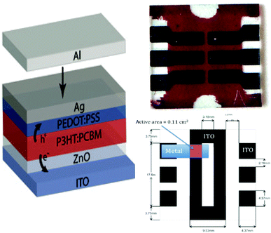
Pre-patterned ITO (Thin Film Devices) was cleaned by sonication in acetone and isopropanol followed by a 5 min exposure to oxygen plasma with a power setting of 145 W (Technics). A ∼35 nm film of ZnO was deposited in air from a diethyl zinc precursor solution. The ZnO film was rinsed with H2O, acetone, and isopropanol to remove residual organics and dust, then dried in a nitrogen stream. Poly(3-hexylthiophene) (P3HT; Plexcore OS 2100) and PCBM (Nano-C) were blended in a 1:0.8 ratio by weight (36 mg ml−1 total concentration) in anhydrous dichlorobenzene (Aldrich) and allowed to stir overnight at 65 °C. In a nitrogen glovebox (<5 ppm O2, <5 ppm H2O), the active layer was spin cast at 600 rpm, placed in a covered Petri dish while still wet, and allowed to slow dry over the course of 90 min resulting in a 220 nm thick layer. The active layer was exposed to oxygen plasma for 0.25 min at a power setting of 45 W. Immediately after the plasma treatment, two layers of PEDOT:PSS (Clevios P VP Al 4083) were consecutively spin cast at 4000 rpm in air followed by a single 10 min anneal at 110–120 °C in a nitrogen glovebox to make a 40 nm hole transport layer. Metal electrodes (Ag 100 nm then Al 100 nm) were thermally evaporated through a shadow mask to yield a device area of 0.11 cm2. The metal evaporator (Angstrom Engineering) employs a water cooled, rotating sample stage and the base pressure during thermal deposition (1–5 Å s−1) is better than 10−7 Torr. The devices are annealed inside a nitrogen glovebox at 130 °C for 15 min.
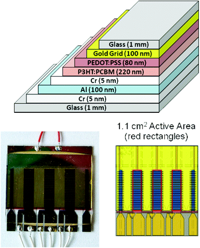
:PSS. Devices were prepared on silica nitride (SixNy) coated glass substrates. SixNy provides a reproducible surface for ink jet printing on a range of substrates. The design structure, complete device and electrodes dimensions are shown in Fig. 4. The active area of the devices was around 3.75 cm2.
 | ||
| Fig. 4 HOLST polymer device, design, and architecture. | ||
All layers, except cathode evaporation, were fabricated in ambient atmosphere. The SunTronic silver nanoparticle ink has been used for the inkjet printing of the current collecting grids. Immediately after printing the substrates were placed in a temperature controlled oven for 30 min at 135 °C. For the inkjet printing a FujiFilm Dimatix Materials Printer (DMP 2831) with 10 pl drop size print heads is used. High conductivity Orgacon™ PEDOT:PSS from Agfa-Gevaert was inkjet printed to give a ∼160 nm thick layer. The photoactive layer was fabricated using 4 wt.% P3HT:[C60]PCBM solution in o-dichlorobenzene. P3HT was purchased from Plextronics, Plexcore OS 2100 and [C60]PCBM (99%) from Solenne BV. The mixing ratio was 1:1 by weight. The active layer was spin-coated at 1000 rpm to give a ∼220 nm thick layer. The samples were subsequently heated at 130 °C for 10 min to achieve an optimal morphology. The metal cathode (1 nm LiF, 100 nm Al) was thermally evaporated in a vacuum chamber through a shadow mask. The finished OPV devices were encapsulated with stainless steel lids using Huntsman Araldite® 2014-1 sealer.
Glass substrates of size 50 mm × 50 mm are cleaned in a sequence of 5 min ultrasonic baths: Acetone (2×), Isopropanol (2×), followed by DI water, then dried with Nitrogen and annealed at 120 °C for 20 min. Evaporation of first electrode (electron contact) Cr/Al/Cr (thickness of 5/100/5 nm) is completed in vacuum. The active layer is spin coated from a blend of P3HT:PCBM = 20 mg:14 mg ml−1 in o-Xylol. The blend solution is heated to 55–60 °C for 15–20 min and then cooled for 15–30 min to prevent gelification and spin cast on the fly at 500 rpm resulting in a final film thickness of 220 nm. PEDOT:PSS (CPP 105 DM, H.C. Starck) is used as a hole transport layer. It is spin coated from a puddle accelerated to 3000 rpm, resulting in an 80 nm thick layer. Samples are annealed at 80 °C for 15 min inside the glovebox (under nitrogen) prior to evaporation of the second electrode (hole contact) with a Cr/Au (support 5/80 nm) and Au (Grid 100 nm). Cells were annealed at 120 °C for 10 min and left inside a glovebox for cooling overnight. Encapsulation was done by using glass (prepared similarly to the substrate) and Delo glue (DELO LP 655). Glue was applied diagonally over the top surface of cleaned (top) glass and attached to the organic solar cell. Pressure was applied through clamps to get homogeneous distribution of glue. The encapsulated cell was exposed to UV radiation (Xenon lamp) for no more than 2 min to cure the glue. Cells were left inside the glovebox for 24 h.
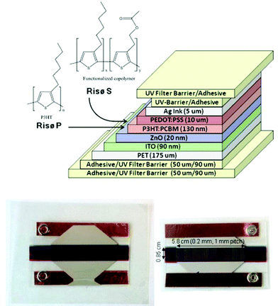 | ||
| Fig. 6 RISØ P and RISØ S polymer device, design, and architecture. | ||
The active layer P3HT (BASF, Sepiolid P200) and PCBM (Solenne B.V.) followed with slot-die coating from a custom low volume slot die coating head allowing a range of ratios of P3HT:PCBM in chlorobenzene to be prepared along the roll. The active layer was coated 130 nm thick and baked at 140 °C. The cells used in this study represent a 1:1 ratio which gave the optimal performance. A hole transport layer, PEDOT:PSS (EL-P 5010, Agfa), was adjusted to a viscosity of 270 mPa s using isopropanol and slot die coated 10 microns thick and baked at 140 °C. The silver back electrode was screen printed with UV curing ink (Toyo, FS18). Cu tape (3M) was applied for electrical connections with metal snap fasteners. Devices were encapsulated using a UV filter/barrier (Amcor) with a pressure sensitive adhesive (467 MPF, 3M) and a full 1 cm edge seal.
2.3 Degradation testing conditions and protocols
It is well known that small changes in the testing environment can have substantial impacts on the performance of OPV devices. One goal of this collaboration was to evaluate the variety of cells under clearly comparable conditions at one site and one time. Three distinct conditions were selected. These conditions are in accordance with ISOS-3 guidelines for stability testing.3 The accelerated full sun simulation was run AM1.5G (1000 W m−2, 85 ± 5 °C, metal halide lamp, KHS Solar Constant 1200) in accordance with ISOS-L-1. An indoor low light test was run under a bank of fluorescent lamps (100 W m−2, Osram FQ Lumilux HO, T∼45 °C) in accordance with ISOS-Low Light-1. A dark storage test was carried out in accordance with ISOS-D-1 Shelf. Daily measurement of the dark storage sample was made with a full sun simulator for a period of 20 min under AM1.5G (1000 W m−2, metal halide lamp, KHS Solar Constant 575). In addition dark curves were collected every two hours, between which the cells were open circuit. All illumination sources were characterized with both a pyranometer (Kipp & Zonen, CM 4) and a calibrated fiber optic spectrometer (Avantes, Avaspec). Room humidity was uncontrolled ambient, and temperature was monitored periodically viathermocouple on the back of the devices. Due to the large number of devices and geometries, no masks were applied in this study. Active areas were defined by electrode geometries provided by cell manufacturers, and no spectral mismatch factors were applied. The calibrated spectra for the full sun simulator and the fluorescent lamps are shown in comparison with AM1.5G in Fig. 7. | ||
| Fig. 7 Irradiance of illumination sources used in this study. | ||
There are several complexities when setting up automated measurements on so many different device types. ISE and RISØ devices had electrical connectors to the thin film electrodes, while other devices had exposed metal contact pads. In most cases subminiature alligator clips (Hirschmann) were employed. This works best with an additional layer of silver paint or epoxy to minimize the scratching of the thin evaporated metal electrodes over time. Fully automated IV characterization was performed on devices under illumination at either 10 or 15 min intervals with a pair of custom built multiplexing systems, each controlling a sourcemeter (Keithley 2400) and a 40 × 2 channel switching relay matrix (Keithley 2700) under computer control. Devices were open circuit between measurements. The graphical abstract shows the array of devices mounted under the full sun simulator. The setup for the indoor low light fluorescent lamps was similar. The ISOS protocols define performance at four times, T0, TS0, T80, and TS80. These times correspond to the initial manufacture date, the time when a stabilized initial performance is recorded, and then times when the performance has dropped to 80% of these values. Since most of the devices were manufactured and shipped from different sites with different initial characterization facilities, we cannot confidently report T0, and T80 as defined. Our study thus reports data in terms of TS100, TS80, TS50, and TS10, where we have named the local peak performance time during the early stages of the measurements as TS100, (rather than TS0) and the other values are all relative to that performance. In this way all measurements are suitable for comparison. Three devices of each type were followed under each condition, until TS80, and a fourth device was also characterized at TS100. One device of each type was pulled from the degradation study at roughly TS100, TS80, TS50, and TS10 to be used in a series of imaging and analytical studies, which are the subject of future publications.
3. Stability data
3.1 Accelerated full sun degradation test
The degradation was dramatically different for the devices in the accelerated full sun simulation environment. The PCE over time is plotted in Fig. 8 for one cell of each device type. This represents the best performance of the devices of each type, but the homogeneity of the devices is quite good at this scale. This is shown in Fig. 9 for the first 400 h of degradation of four RISØ P devices (a), and for the first 50 h of degradation of six IMEC devices, including two (labelled E) which were encapsulated. The NREL, HOLST, and RISØ P devices were removed for further analysis after reaching TS10. The remaining cells ran over 1800 h before removal for analysis. The full set of degradation curves for each of the devices is available in the supplementary data associated with this article.† | ||
| Fig. 8 Efficiency of all device types versus time under accelerated full sun illumination. | ||
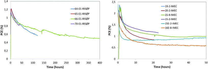 | ||
| Fig. 9 Efficiency of RISØ P (left) and IMEC (right) devices versus time during initial burn-in under full sun illumination. | ||
In some cases it was possible to look at devices both with and without encapsulation, either by removing the encapsulation, or by having a second set of devices prepared. The process of removing the encapsulation can damage the device, and degrade the performance.
We were able to remove encapsulation from the IAPP and HOLST devices, and a second set of IMEC devices were prepared with encapsulation. The IAPP devices showed both an initial drop in performance and degradation over time after removing the encapsulation, as can be seen in the supplementary data.† The HOLST device without encapsulation performed quite similarly to the encapsulated devices suggesting the degradation here is not due to atmospheric components. As seen in the early time data of Fig. 9b, the encapsulated IMEC cells did not appear to be more stable during the first 50 h, but do show recovery over longer time scales as can be seen in the supporting information Figure S1† where the encapsulated cell initially drops below the unencapsulated cell, but then shows a steady rise by almost a factor of two over a thousand hours. This phenomenon cannot be fully explained, but the samples are undergoing further analysis, and an experiment with a larger number of encapsulated samples could establish its relevance and origin.
3.2 Low level indoor fluorescent light degradation test
Most of the devices performed much better in the low light study, as can be seen in Fig. 10. The NREL degradation curve is marred by noise believed to be due to problems with the contacts. The PCE values were measured using the fluorescent light and an estimation of 100 W m−2, but the spectral response of the cells is not included. Different cells of each device type were very consistent, as can be seen in the supplementary data.† | ||
| Fig. 10 Efficiency of all device types versus time under fluorescent illumination. | ||
3.3 Dark storage with daily full sun characterization
The trade off between true dark storage with no characterization and dark storage with periodic illumination for characterization is difficult. The data from our measurements over 1800 h are shown in Fig. 11. The complete set of measurements is available in the supplementary data.† | ||
| Fig. 11 Efficiency of all device types versus time measure periodically under full sun illumination with dark storage. | ||
4. Discussion
4.1 Quantitative measurements
The data shown in Fig. 8–11 and Figures S1-S8 in the supplementary data† are the detailed characterization of the devices, but cannot provide easy reference points for comparison.Each graph contains the results of thousands of measured data points, and invariably there are some (∼5) glitches in each dataset where the curves would have isolated nonsensible values. We have omitted such points from the plots for clarity, but no smoothing has been applied to the data sets. Table 2 displays the initial PCE values for the devices at TS100, and the TS80, TS50, and TS10 values that can be obtained from our data for all the devices under all three lighting conditions. PCE values are reported for a device which is in the middle range of a given set, and T values are taken from a single sample which is typically the most stable device in each set.
| IAPP | IMEC | NREL | HOLST | ISE | RISØ P | RISØ S | |
|---|---|---|---|---|---|---|---|
| a Please see ref. 3 for an in depth explanation of TS100. Briefly it is the initial stabilized performance to which lifetime data is referenced. | |||||||
| Full sun | |||||||
| T S100 (PCE,%) | 2.15 | 2.28 | 2.82 | 0.97 | 2.63 | 1.22 | 1.58 |
| T S80 | >1800 | 1 | 0.5 | 37 | 5 | 40 | 23 |
| T S50 | >1800 | 13 | 41 | 72 | 510 | 295 | 181 |
| T S10 | >1800 | >1800 | 110 | 136 | >1800 | 1539 | >1800 |
| Low light | |||||||
| T S100 (PCE,%) | 2.01 | 2.08 | 2.81 | 2.05 | 4.18 | 0.61 | 0.51 |
| T S80 | >1800 | 17 | 380 | >1800 | 189 | 13 | 4 |
| T S50 | >1800 | 115 | 889 | >1800 | >1800 | 42 | 161 |
| T S10 | >1800 | >1800 | >1800 | >1800 | >1800 | 620 | 891 |
| Dark storage | |||||||
| T S100 (PCE,%) | 1.86 | 2.19 | 2.24 | 0.88 | 2.56 | 0.68 | 0.71 |
| T S80 | >1800 | 183 | 305 | >1800 | >1800 | 1312 | 305 |
| T S50 | >1800 | 711 | 686 | >1800 | >1800 | >1800 | 1360 |
| T S10 | >1800 | >1800 | >1800 | >1800 | >1800 | >1800 | >1800 |
4.2 IAPP degradation
The IAPP devices were remarkably stable in all three illumination conditions as shown in Figure S2.† There is no discernable degradation over 1800 h even when compared with Si photodiodes used to monitor the accelerated full sun simulator (Hammamatsu, S5911) or the dark storage environment (Hammamatsu, S1136).The only degradation observed in the IAPP samples was after the removal of the encapsulation. IAPP devices showed an initial decay upon breakage of the epoxy used in the encapsulation associated with damage to the contacts. However devices where this contact was maintained or repaired still show linear degradation suggesting that the encapsulation plays a significant role in the stability of these devices.
In contrast to devices with wet processing of layers, in the IAPP devices all layers are deposited viathermal evaporation in vacuum. This makes these devices thermally stable, even in our accelerated full sun environment. They are also the only devices encapsulated with a getter giving them the best protection from oxygen and water infiltration when properly sealed.
4.3 IMEC degradation
The IMEC devices degraded under accelerated full sun simulation present a sharp decrease of ∼60% in efficiency over the initial 50 h of the illumination. This initial burn-in is a combined effect of the decrease of all the JV parameters. In the next stage of the degradation these parameters stabilize until ∼1200 h, where we observe a gradual decrease of the FF.Devices degraded under low level indoor fluorescent light present a sharp decrease in efficiency of ∼50% in the first 100 h. This burn-in stems from the rapid exponential decrease of the Jsc, then the decay becomes linear. Other JV parameters, namely Voc and FF remains stable over 1500 h.
Devices degraded in dark storage condition present a burn-in over ∼500 h after which the failure slows down. This decrease stems mainly from the decrease of the Jsc, while the Voc and FF remain stable over 1500 h.
The various illumination conditions result in similar stabilized initial efficiencies for the IMEC devices although the time period required for the stabilization differs, as shown in Figure S3.† The decrease represented on a logarithmic scale (see inset) clearly shows that the initial burn-in under full sun occurs over ∼20–50 h, while under fluorescent illumination over ∼200 h and finally in dark (with daily illumination for measurement) over ∼1000 h. The normalized IV properties under each condition indicate that in case of dark and low light intensity illumination, the same mechanism takes place and light acts as acceleration factor. In contrast the accelerated full sun illumination which also contains UV light and a higher temperature seems to activate other mechanisms simultaneously as both FF and Voc decay with Jsc contributing to the faster initial drop in efficiency. Measurements on identical devices under full sun illumination performed on a cooled stage at IMEC for up to 500 h display a qualitatively comparable burn-in, though the drop only counts for ∼40% and occurs on a longer time scale. This difference in sample temperature is substantial with T ∼73 °C without the cooling stage, and ∼40 °C with active cooling.
4.4 NREL degradation
The NREL devices show almost identical degradation under the low level indoor fluorescent light and dark storage conditions, degrading to TS50 in less than 900 h as seen in Figure S4.† The degradation under fluorescent illumination is driven by changes in Voc and FF, not Jsc, while all three parameters contribute to the degradation in dark storage. Under accelerated full sun simulation the degradation is substantially faster, and appears to have two linear regimes: initially degrading to TS60 in ∼4 h, and then decaying to TS10 by ∼100 h. This degradation in PCE correlates with a decay in Jsc and FF for these devices, while the Voc is relatively stable. The NREL devices were easily scratched by contact clips to the electrodes and this is seen as noise in the data.The degradation reported here is substantially greater than for similar devices measured at NREL. There are several differences that in combination may account for this. One is the illumination source, which emits more UV and creates a much higher temperature environment for the accelerated full sun measurements. Measurements under a sulphur plasma lamp with negligible UV output at NREL have samples typically reaching TS90 in 50 h, and TS50 in 550 h. Under a solar simulator with more UV output at NREL similar samples reach TS90 in ∼20 h, and TS65 in 225 h with substrate temperatures of 45 °C. Whereas in the RISØ accelerated full sun condition the NREL samples were measured to be 76 °C resulting in much faster degradation. The ISOS dark storage test involves a daily exposure to a similar lamp for ∼20 min, and that exposure may be doing more damage than the longer dark storage period for these devices. This would not affect the devices under the low level indoor fluorescent illumination. However, in those measurements the electrical contacts were problematic. This is an area which will be addressed in future inter-laboratory collaborations.
4.5 HOLST degradation
The HOLST devices were extremely stable in both dark storage and low level indoor fluorescent light. There was no initial burn-in in either case. In marked contrast these devices degrade completely under accelerated full sun simulation as seen in Figure S5.† The degradation to TS80 takes ∼40 h and after an additional 100 h they reach TS10 in a fairly linear process with no stabilized plateau. The full sun degradation was the same in the encapsulated samples and in samples that were opened prior to soaking, suggesting that the mechanism may be a single process due to a thermal instability at 75 °C. Identically prepared devices were exposed at HOLST under a halogen lamp at 1 sun at 45 °C, and were very stable (TS90 > 1000 h), but when exposed with higher temperature (85 °C), the devices again degraded very fast.4.6 Fraunhofer ISE degradation
The Fraunhofer ISE devices stabilized near TS80 in both dark storage and low level indoor fluorescent light during the first 1000 h as seen in Figure S6.† Particularly striking was the high PCE values (4.2%) recorded by these devices under low level indoor fluorescent light, almost 60% higher than the same devices in the other two conditions (2.6%). Under accelerated full sun simulation a rapid degradation to TS65 occurs over 50 h followed by a slower linear degradation toward TS10 over 2000 h with no stabilized plateau. This degradation is mirrored in Jsc and an initial decay in FF from 65% to 35% over 500 h. The degradation in dark storage and fluorescent illumination is almost entirely from the change in Jsc.In degradation experiments on similar devices performed at Fraunhofer ISE under continuous illumination (Sulphur plasma lamp and 50 °C), Jsc is remarkably stable and the main loss in PCE is correlated with a loss in FF. For Jsc, the Fraunhofer ISE experiments observe a significant burn-in on a 50 h timescale and recovery during the first couple of hundred hours to nearly the initial value. This difference is probably related to the different lamps and temperatures used. Under thermal (85 °C) and UV stress Fraunhofer ISE measurements do observe a significant decrease in Jsc.
4.7 RISØ P degradation
It is evident that the RISØ P devices show a rapid initial exponential decay followed by a linear decay both in the accelerated full sun and indoor fluorescent illumination conditions as seen in Figure S7.† In both cases the degradation is observed in Jsc, FF, and even in Voc. In contrast the dark storage condition appears to be more stable with a more modest linear decay and no obvious exponential decay.Similar devices have been manufactured as modules with 16 stripe cells in series as part of the demonstration workshops at ISOS-3, and were more stable under similar illumination conditions for periods of 1000 h. The workshop modules showed comparable initial PCE values, but only a modest linear degradation under full sun simulation with TS80 ∼800 h (20 times the TS80 of the RISØ P cells) and no discernable degradation under the same indoor fluorescent illumination (i.e. TS80 >100 times the RISØ P cells). A focus at RISØ has been on the development of stable R2R modules on flexible substrates, but cells were manufactured in this case for better comparison with the devices from other laboratories.
To explain the difference in degradation of these cells and the modules we consider two types of causes: a fundamental difference in the device geometry which influences the stability or a deficiency in the processing.
The geometric differences are substantial, between the 35.5 cm2 active area of the 16 cell module and the 4.9 cm2 active area for the individual cells in this study. In addition, the cell has a comb electrode, while cells in the module have a full silver electrode. This means that for the individual cells we are counting on the PEDOT:PSS layer to transport positive charge carriers laterally up to 500 um, while in the full silver module geometry the PEDOT:PSS layer need only transport charges 10 um across the layer thickness. PEDOT:PSS has been reported to influence device degradation as it takes up water and can lead to oxidation of electrodes.
The processing of the samples was very similar, with the most notable difference being in the coating speed of the ZnO nanoparticle layer. In the workshop modules this coating speed was 2 m min−1, while the individual RISØ P cells were coated at twice that speed, 4 m min−1. In a R2R process the coating speed is inversely proportional to the bake time, and the shorter bake time is suspected to have reduced the adhesion of the ZnO nanoparticles to the ITO, resulting in a less effective electron transport layer. Additional evidence for the deficiency in the ZnO layer is that the RISØ P cells did not maintain the photoactivation of the ZnO nanoparticles. This may explain why the RISØ cells (S and P) were the only cells to degrade faster under the fluorescent illumination than under the accelerated full sun simulation where there is substantially more UV light. The presence of the UV filter in these devices makes it much more difficult to maintain the activation the ZnO thus accelerating the degradation in PCE.
4.8 RISØ S degradation
The only intentional difference between RISØ S and RISØ P is in the active layer. RISØ S devices degraded under all three illumination conditions as seen in Figure S8.† They showed a slightly better stability under accelerated full sun illumination after 900 h compared to RISØ P. In the dark storage condition the RISØ S devices degraded smoothly without a burn in plateau, as seen with RISØ P devices. Under low level indoor fluorescent lighting the degradation is qualitatively the similar for RISØ S and RISØ P.Under full sun illumination the degradation is due to decay of both Jsc and FF. Under the low level indoor fluorescent illumination the degradation is seen in Jsc, but the rise in PCE near 100 h is correlated with an improvement in FF which then stabilizes. The degradation in dark storage is correlated with a decay in Jsc.
4.9 Commentary across sample types
The IAPP evaporated small molecule cells with full glass encapsulation are extraordinarily stable under all our test conditions. This technology is significantly different from all the other device types as the organic photo-active materials and transport layers are evaporated in a vacuum process, rather than wet coating processes common in all the other devices.Although all other cells incorporate a P3HT:PCBM blend of comparable thickness as active layer, device failure considerably differs under full sun accelerated ageing as compared in Fig. 9. The only common trend across the different samples is that decrease in efficiency occurs in a two-stage process with a fast initial drop followed by a stabilization and slow linear decrease. Interestingly, both the timescale and quantitative decrease considerably varies among different devices, indicating that transport layer and electrode materials as well as device processing conditions influence device failure.
Encapsulated devices (IAPP, HOLST, ISE, and RISØ) demonstrated excellent stability in the dark storage testing as expected if degradation is related to reactivity with water and oxygen from the ambient atmosphere. It should be noted that the unencapsulated devices from NREL and IMEC were measured at the home laboratory immediately after fabrication and at the beginning of the study at RISØ DTU. While the stability in the tables and figures reported here is entirely from the measurements after devices arrived at RISØ DTU to eliminate potential measurement differences across laboratories, we note average NREL devices appear to have dropped from 2.6% to 2.3% during this one month phase and IMEC devices appear to have dropped from 3.2% to 2.2%. The encapsulated devices do not demonstrate significant degradation in similar measurements.
The standard ITO transparent conductor is both expensive and brittle. Devices from HOLST and ISE have replaced ITO with PEDOT:PSS hole transport layers capped by Ag and Au grids, respectively. Both device types displayed excellent stability in dark and low light illumination showing real promise for these architectures. The difference in performance under accelerated full sun illumination was dramatic, and could be due to the 15 °C difference in cell temperatures, as the polymer layers are quite similar in both devices.
There has been extensive discussion that the hygroscopic nature of PEDOT:PSS and its tendency to phase separate contribute to degradation in many devices. The IAPP and IMEC devices in this study eliminate PEDOT:PSS substituting DF-DPB:C60F36 and MoO3 respectively for the hole transport layer. The IAPP data suggest DPB:C60F36 works well (at least when encapsulated) and while the IMEC samples do show a very fast initial degradation, they stabilized with the highest efficiency of all the P3HT:PCBM devices after 900 h under accelerated full sun illumination.
Four of the devices in this study (IMEC, NREL, RISØ S, and RISØ P) use ZnO as an electron transport layer. All of them display a fast degradation to TS50 under accelerated full sun illumination. All but the NREL devices show a similarly fast degradation under low level indoor fluorescent lighting. This result indicates that minor differences in the processing routes of ZnO are critical for device lifetime.
4.10 Sample optimization
In a single laboratory study, the samples are refined and measured in a cyclic process and the results are disseminated. In our study, each laboratory had already demonstrated the ability to produce unique high quality OPV samples, and one set was created for this study. Despite careful planning some details could be better optimized. Most notably, for a long term stability study with samples moving between many laboratories, it is essential that electrical contacts be stable and robust to multiple mounting measurement cycles. When possible it is desirable to have both encapsulated and bare devices for comparison. The active area for the different devices varies significantly in this study and while no preference should be given for small or large device areas it is advisable to compare devices with similar active area and perhaps include both small devices with careful masking and larger devices where masking is not so critical. Where possible it would be interesting to compare different device architectures with identical encapsulations for direct comparison, just as this study provided identical illumination environments. It is likely that in order to achieve economic viability OPV technology must eventually move to flexible substrates, and while only the RISØ devices were flexible in this study, many laboratories are now making some devices on flexible substrates, which would be interesting to compare side by side in a future study similar to the one performed here.4.11 Further studies
The number of experimenters, timeline, device type, number of devices and experimental conditions employed in this study is very large and this report comprises the first in a series with the aim of achieving consensus on OPV stability studies in a broad sense. The data collection was planned such that detailed analysis is possible. In addition to this qualitative and comparative degradation study all the devices were imaged using several techniques which will be reported in a separate communication. The image data shows specific degradation phenomena and is coupled to careful analysis of the chemistry at specific locations using a series of chemical probe techniques which will also constitute a separate report. Finally, the degradation was followed with physical probes for functionality such as IPCE measurements and this will be reported as a final communication in the series of four papers.5. Conclusions
State of the art polymer solar cells were fabricated at leading laboratories and characterized under identical conditions in an extensive inter-laboratory collaboration planned at the ISOS-3 summit. Degradation of cells under three distinct illuminations is reported for seven different cell types. This is part of an ongoing study where several specialized techniques are being applied uniformly by leading research groups on these same cells at different stages of their degradation. It is believed that this will give us unprecedented insight into the chemical and physical phenomenon that govern the degradation of polymer solar cells and will provide substantial knowledge for the research community in this field.Furthermore, this experiment highlights the difficulty of comparing lifetime data between laboratories as even slight differences and neglected details in ageing conditions impact device lifetime. This large-scale experiment not only establishes the first public lifetime database but further paves-the-way towards novel approaches to conduct reliability experiments.
Acknowledgements
This work has been supported by the Danish Strategic Research Council (2104-07-0022), EUDP (j.no. 64009-0050) and the Danish National Research Foundation. Partial financial support was also received from the European Commission as part of the Framework 7 ICT 2009 collaborative project HIFLEX (grant no. 248678), partial financial support from the EUIndian framework of the ‘‘Largecells’’ project that received funding from the European Commission’s Seventh Framework Programme (FP7/2007–2013. grant no. 261936), partial financial support was also received from the European Commission as part of the Framework 7 ICT 2009 collaborative project ROTROT (grant no. 288565) and from PVERA-NET (project acronym POLYSTAR).References
- M. Jørgensen, K. Norrman and F. C. Krebs, Sol. Energy Mater. Sol. Cells, 2008, 92, 686–714 CrossRef.
- C. J. Brabec, S. Gowrisanker, J. J. M. Halls, D. Laird, S. Jia and S. P. Williams, Adv. Mater., 2010, 22, 3839–3856 CrossRef CAS.
- M. O. Reese, S. A. Gevorgyan, M. Jørgensen, E. Bundgaard, S. R. Kurtz, D. S. Ginley, D. C. Olson, M. T. Lloyd, P. Morvillo, E. A. Katz, A. Elschner, O. Haillant, T. R. Currier, V. Shrotriya, M. Hermenau, M. Riede, K. Kirov, G. Trimmel, T. Rath, O. Inganäs, F. Zhang, M. Andersson, K. Tvingstedt, M. Lira-Cantu, D. Laird, C. McGuiness, S. Gowrisanker, M. Pannone, M. Xiao, J. Hauch, R. Steim, D. F. M. DeLongchamp, R. Rösch, H. Hoppe, N. Espinosa, A. Urbina, G. Yaman-Uzunoglu, J.-B. Bonekamp, A. J. J. M. van Breemen, C. Girotto, E. Voroshazi and F. C. Krebs, Sol. Energy Mater. Sol. Cells, 2011, 95, 1253–1267 CrossRef CAS.
- F. C. Krebs, S. A. Gevorgyan, B. Gholamkhass, S. Holdcroft, C. Schlenker, M. E. Thompson, B. C. Thompson, D. Olson, D. S. Ginley, S. E. Shaheen, H. N. Alshareef, J. W. Murphy, W. J. Youngblood, N. C. Heston, J. R. Reynolds, S. Jia, D. Laird, S. M. Tuladhar, J. G. A. Dane, P. Atienzar, J. Nelson, J. M. Kroon, M. M. Wienk, R. A. J. Janssen, K. Tvingstedt, F. Zhang, M. Andersson, O. Inganäs, M. Lira-Cantu, R. de Bettignies, S. Guillerez, T. Aernouts, D. Cheyns, L. Lutsen, B. Zimmermann, U. Würfel, M. Niggemann, H.-F. Schleiermacher, P. Liska, M. Grätzel, P. Lianos, E. A. Katz, W. Lohwasser and B. Jannon, Sol. Energy Mater. Sol. Cells, 2009, 93, 1968–1977 CrossRef CAS.
- S. A. Gevorgyan, A. J. Medford, E. Bundgaard, S. B. Sapkota, H. F. Schleiermacher, B. Zimmermann, U. Wurfel, A. Chafiq, M. Lira-Cantu, T. Swonke, M. Wagner, C. J. Brabec, O. Haillant, E. Voroshazi, T. Aernouts, R. Steim, J. A. Hauch, A. Elschner, M. Pannone, M. Xiao, A. Langzettel, D. Laird, M. T. Lloyd, T. Rath, E. Maier, G. Trimmel, M. Hermenau, T. Menke, K. Leo, R. Rösch, M. Seeland, H. Hoppe, T. J. Nagle, K. B. Burke, C. J. Fell, D. Vak, Th. B. Singh, S. E. Watkins, Y. Galagan, A. Manor, E. A. Katz, T. Kim, K. Kim P.M. Sommeling, W. J. H. Verhees, S. C. Veenstra, M. Riede, G. M. Christoforo, T. Currier, V. Shrotriya, G. Schwartz and F. C. Krebs, Sol. Energy Mater. Sol. Cells, 2011, 95, 1398–1416 CrossRef CAS.
- M. Hermenau, M. Riede, K. Leo, S. A. Gevorgyan, F. C. Krebs and K. Norrman, Sol. Energy Mater. Sol. Cells, 2011, 95, 1268–1277 CrossRef CAS.
- E. Voroshazi, B. Verreet, A. Buri, R. Muller, D. Di Nuzzo and P. Heremans, Org. Electron., 2011, 12, 736–744 CrossRef CAS.
- M. T. Lloyd, C. H. Peters, A. Garcia, I. V. Kauvar, J. J. Berry, M. O. Reese, M. D. McGehee, D. S. Ginley and D. C. Olson, Sol. Energy Mater. Sol. Cells, 2011, 95, 1382–1388 CrossRef CAS.
- Y. Galagan, J. E. J. M. Rubingh, R. Andriessen, C. C. Fan, P. W. M. Blom, S. C. Veenstra and J. M. Kroon, Sol. Energy Mater. Sol. Cells, 2011, 95, 1339–1343 CrossRef CAS.
- B. Zimmermann, U. Würfel and M. Niggemann, Sol. Energy Mater. Sol. Cells, 2009, 93, 491–496 CrossRef CAS.
- J. Alstrup, M. Jørgensen, A. J. Medford and F. C. Krebs, ACS Appl. Mater. Interfaces, 2010, 2819–2827 CAS.
- F. C. Krebs, S. A. Gevorgyan and J. Alstrup, J. Mater. Chem., 2009, 19, 5442–5451 RSC.
Footnote |
| † Electronic supplementary information (ESI) available: Lifetime data for IMEC devices with and without encapsulation, normalized lifetime data for all devices comparing accelerated full sun, low light and dark storage conditions. See DOI: 10.1039/c1ra00686j |
| This journal is © The Royal Society of Chemistry 2012 |