DOI:
10.1039/C1RA00642H
(Paper)
RSC Adv., 2012,
2, 1450-1456
Solvothermal synthesis and growth mechanism of ultrathin Sb2Te3 hexagonal nanoplates with thermoelectric transport properties†
Received
28th August 2011
, Accepted 29th October 2011
First published on 19th December 2011
Abstract
Uniform single-crystalline hexagonal-shaped Sb2Te3 nanoplates with a thickness of 30–40 nm have been successfully synthesized by a glucose-assisted solvothermal process in the mixed solvents of ethanediamine and water. It is found that the reaction time, concentration of glucose, reaction temperature and the volume ratio of ethanediamine to water play important roles in the formation of the uniform Sb2Te3 nanoplates. Based on the experimental results, the possible reaction process and formation mechanism of these hexagonal nanoplates is proposed. Different from previous reports, the growth process of such Sb2Te3 nanoplates can be reasonably explained by a self-assembly process and an Ostwald ripening mechanism. The thermoelectric transport properties are investigated by measuring the electrical conductivity and the Seebeck coefficient in the temperature range of 300–600 K. The samples show much more enhanced Seebeck coefficients than that of bulk Sb2Te3. Meanwhile, the size of the sample has much impact on both the electrical conductivity and the Seebeck coefficient.
Introduction
In the past few decades, nanostructured materials of specific morphologies have attracted much attention due to their morphology and size dependent properties.1–3 Until now, numerous nanomaterials with different morphologies and sizes, such as nanowires, nanotubes, nanoplates, nanosheets etc., have been fabricated.4–9 And versatile synthetic strategies have been developed to achieve such nanomaterials, including thermolysis of various metallic precursors, solvothermal/hydrothermal processes, electrochemical deposition technique, chemical vapor deposition and the hot-injection methods. Among these methods, the solvothermal/hydrothermal process is one of the most popular methods for controllable synthesis of nanomaterials with different sizes and morphologies.
Antimony telluride (Sb2Te3) based compounds are very promising materials for room-temperature thermoelectric applications. Recent studies suggest that materials with nanostructures have higher figures-of-merit (ZT) due to both a high density of states and an increased phonon scattering or reduced lattice thermal conductivity in the nanosystems.10,11 For instance, the p-type nanostructured thin film superlattices of Bi2Te3 and Sb2Te3, grown from chemical vapor deposition, have ZT values of about 2.4 at room temperature.12 This result greatly stimulated interest in the synthesis of Sb2Te3 nanostructures with well-controlled morphologies and sizes. Therefore, Sb2Te3 based nanomaterials with different morphologies and sizes have been synthesized by various methods. For instance, previous work reported that Sb2Te3 hexagonal nanoplates had been fabricated through rapid microwave-assisted wet chemical13 and hydrothermal/solvothermal routes.14,15 A vapor–liquid–solid growth method16,17 and electrochemical deposition route have been employed to prepare arrays of Sb2Te3 nanowires.18 Sb2Te3 nanorings19 and nanobelts20 have been synthesized by a simple hydrothermal process. Although many methods have been applied for the synthesis of Sb2Te3 hexagonal nanoplates, limited reports have been involved with the synthesis of hexagonal nanoplates with thicknesses less than 50 nm and the detailed formation mechanism.
Herein, we report the fabrication of Sb2Te3 hexagonal nanoplates through a facile solvothermal method with the assistance of glucose. Some factors affecting the morphologies of Sb2Te3 crystals, such as reaction time, concentration of glucose, reaction temperature, and the volume ratio of ethanediamine to water are systematically investigated. On the basis of time-dependent SEM observations, a formation mechanism different from those previously reported for such hexagonal nanoplate morphology is proposed, which is related to self-assembly and an Ostwald ripening process. In addition, the diameter and thickness of the nanoplates can be tuned by adjusting the concentration of glucose. Moreover, the size-dependant thermoelectric transport properties are clearly demonstrated, which present much enhanced Seebeck coefficients as compared to that of bulk Sb2Te3.
Experimental section
In this work, all the solvents and chemicals were purchased from Shanghai Chemical Reagent Co. and used without further purification unless otherwise stated.
Preparation of Sb2Te3 nanoplates
In a typical procedure, 0.135 g of antimony potassium tartrate (K(SbO)C4H4O6·0.5H2O), 0.135 g of sodium tellurite (Na2TeO3·0.5H2O) and 0–0.9 g of glucose were dissolved in 10 mL water, then 20 mL of ethanediamine was added under constant stirring. Subsequently, the resulting solution was transferred into a 40 mL Teflon-lined stainless-steel autoclave. Then the autoclave was sealed and maintained at 180 °C for 12 h. After that, the autoclave was cooled naturally to ambient temperature. The prepared silvery grey products were collected, centrifuged and washed with distilled water and absolute ethanol several times, then dried under vacuum at 80 °C for 12 h.
Characterization
XRD measurements were performed on a Rigaku-D/MAX-2550PC diffractometer, using Cu-Kα radiation at 40 kV, 50 mA, employing a scanning rate of 4° min−1 in the 2θ range from 10° to 90°. The morphologies of the products were characterized by an FEI Quanta 200F field emission scanning electron microscope (FESEM). The fine crystal structures of the particles were detected using transmission electron microscopy (TEM, FEI Tecnai G2 S-Twin operating at 300 kV). Infrared analysis was detected on an FTIR spectrometer (Shimadzu) in the range of 400–4000 cm−1 with the samples mulled in KBr wafers.
Thermoelectric transport measurement
To measure the electrical conductivity and Seebeck coefficient of the as-prepared samples, a pressed bar like sample (10 × 4.6 × 1.2 mm) was prepared under 20 MPa pressure at room temperature. Silver pastes were used as electrical contacts for the electrodes to the specimen. The four-probe method was adopted for the electrical conductivity measurement. For the measurement of Seebeck coefficient, a microheater was applied to create a temperature difference of about 3–15 K between the cool and hot ends of the specimen. A temperature gradient was established in the samples when the electrical power was applied by a thermoelectric pile. The two thermocouples were contacted with the surface of the samples to detect the temperature drop (ΔT), while the resulting thermally induced voltage ΔV was tested by the voltage probes. Then the Seebeck coefficient can be obtained using the formula, S = −ΔV/ΔT. The data of electrical conductivity and Seebeck coefficient were collected by a computer-controlled multifunctional measuring system with a flow of argon of 1 mL min−1 (Keithley 2400 source meter, Keithley 2700 multimeter, Keithley Instruments Inc., America).
Results and discussion
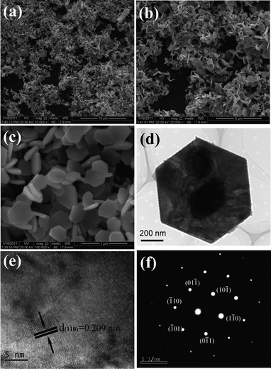
Using the Rietveld refinement method, the crystal structures of Sb2Te3 synthesized at 180 °C for 12 h is refined with the room temperature, high-resolution powder XRD data. Rietveld refinement fitting results are presented in Fig. 1. The experimental intensity data are depicted by a dotted line, while the solid line is the calculated pattern of Sb2Te3. The bottom line represents the difference between the observed and calculated patterns. The refined result is converged to lattice parameters with reliability factors of Rwp = 0.0942 and Rp = 0.0725, thus confirming the presence of Sb2Te3 as a single-crystalline phase in the powder. The morphology and size of the as-prepared samples are studied by FESEM. Fig. 2a shows the overall morphology of a typical sample composed of numerous uniform platelike structures. The magnified SEM images shown in Fig. 2b and 2c clearly display that the obtained products are predominantly hexagonal-based plates, and the edge length of the plates is in the range of 300–500 nm with a thickness of about 30–40 nm. To further investigate the microstructural details of the Sb2Te3 platelike nanostructures, TEM and HRTEM analysis were carried out. Fig. 2d shows the TEM image of typical Sb2Te3 hexagonal nanoplates. Observed carefully, the surface of the nanoplate is rough. The corresponding HRTEM lattice and spot pattern of SAED, shown in Fig. 2e and 2f, demonstrate the single crystalline nature of the nanoplate. The spacing of 0.209 nm is consistent with the lattice spacing of (110) planes of Sb2Te3.
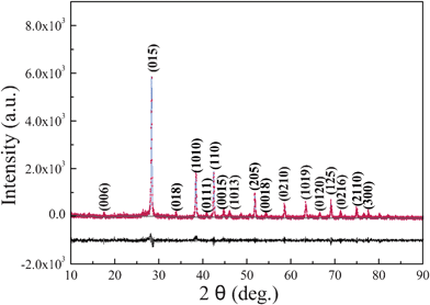 |
| | Fig. 1 Observed and calculated XRD powder profiles for Sb2Te3 with the difference curve shown below. | |
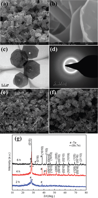 |
| | Fig. 3 The morphology and structure of the Sb2Te3 crystals synthesized in the presence of 0.6 g glucose at 180 °C for different time intervals: (a) low magnification, (b) high magnification SEM images, (c) TEM image, and (d) SAED pattern of the products obtained at 2 h; (e) 4 h; (f) 6 h; (g) XRD patterns. | |
Based on the above experimental results and analysis, the whole morphology evolution process of the Sb2Te3 hexagonal nanoplates is proposed, as illustrated in Fig. 4. In this formation process, time is the key controlling factor. Such a process involves a fast nucleation of amorphous primary particles accompanied by an aggregation and ripening process. In the initial stage, the TeO32− ions are first reduced into element Te, and simultaneously a disproportionation reaction occurs in the alkaline solution, resulting in the formation of Te2− and TeO32− ions. Then the Te2− ions and Sb3+ ions react to form Sb2Te3. When no TeO32− ions are added into the solution, no solid product could be obtained. This result suggests that the Sb(III)(tart) complex can not be reduced to elemental Sb in this reaction system. As depicted above, the reaction process can be formulated as:
| | | TeO32− + H2NCH2CH2NH2 → Te + H2O + OH− | (1) |
| | | 3Te + 6OH− → 2Te2− + TeO32− + 3H2O | (2) |
| | | 3Te2− + 2Sb3+ → Sb2Te3 | (3) |
As the Sb
2Te
3 nuclei are generated, the
glucose molecules will be adsorbed on the surface due to the higher surface energy. Because of the
hydrogen bond and electrostatic effects of
glucose, the capped nuclei are quickly assembled into large plate-like structures. Such capped nuclei assembled into larger entities is similar to those proposed for the formation of crystalline
CaCO3.
21 Zhang's research
groups22 reported that the layered anisotropic lattice structure of Sb
2Te
3 tended to grow along the top–bottom crystalline plane rather than that along the
c-axis, which led to the formation of nanoplates. In our system, the formation of the nanoplate is also attributed to the inherent crystal structure. Because of the high surface energy of the nuclei, the aggregated Sb
2Te
3 particles are not in thermodynamic equilibrium and are metastable, thus, the better crystalline Sb
2Te
3 nanoplates become thermodynamically preferred with the elimination of the
glucose molecules from the nuclei. So the transformation from the poor crystallites to better crystalline Sb
2Te
3 through
Ostwald ripening can be observed. In addition, the packing structure of rhombohedral Sb
2Te
3 viewed along the
c-axis can be described as an infinite hexagon with the composition of alternating
Sb and
Te ions, resulting in the formation of hexagonal platelike crystals. This intrinsic crystal property that dominates the shape of the particles can also be found in the formation of Bi
2Te
3 hexagonal nanoplates.
23 As the
Ostwald ripening process proceeds, the smaller
nanoparticles adsorbed around the plate are consumed and grew gradually to make the nanoplate bigger.
 |
| | Fig. 4 Schematic illustration of the proposed formation mechanism of the Sb2Te3 nanoplates. | |
On the basis of the above experiments results, glucose molecules may promote the aggregation of the Sb2Te3 nanoparticles and affect the crystal growth. To further verify the effects of glucose, the products obtained at different time intervals are characterized by FT-IR spectra, as shown in Fig. S1.† In the first step (2 h), two absorption peaks located at about 3462 and 1650 cm−1 correspond to O–H stretching vibration and C![[double bond, length as m-dash]](https://www.rsc.org/images/entities/char_e001.gif) O stretching vibration, respectively, which demonstrates that the glucose molecules can not be washed off by water and ethanol, indicating the strong interaction between glucose and the nanoparticles. As the reaction time is prolonged, the interaction strength starts to decrease with the crystal growth, that is, the effect of glucose decreases gradually when the Sb2Te3 crystals become more complete.
O stretching vibration, respectively, which demonstrates that the glucose molecules can not be washed off by water and ethanol, indicating the strong interaction between glucose and the nanoparticles. As the reaction time is prolonged, the interaction strength starts to decrease with the crystal growth, that is, the effect of glucose decreases gradually when the Sb2Te3 crystals become more complete.
Influencing factors
For the sake of clarifying the role glucose molecules play in controlling the morphology of the product, we have synthesized the Sb2Te3 micro-platelike structures without the addition of glucose. Fig. 5a and 5b present a SEM image of the prepared sample. From the image, it can be observed that the main product is microplates with an edge length of 4–10 μm and an average thickness of 600 nm, but most of the microplates have irregular shapes. When the dosage of glucose is tuned to 0.3 g, the Sb2Te3 samples remain the same platelike structures except that the length and thickness of the Sb2Te3 samples decrease to 0.5–4 μm and 50–80 nm, respectively, whereas, some hexagonally shaped nanoplates form (Fig. 5c and 5d). With increasing the amount of glucose to 0.6 g, the hexagonally shaped platelike structures become more uniform and the size continues to decrease, as can be seen in Fig. 2a–c. Further increasing the amount of glucose to 0.9 g, the morphology and the size of the samples have little changes. As discussed above, the obtained nuclei can be protected due to the existence of glucose molecules, which slows down the reaction speed. As the mass transport is impeded, the products become smaller and more regular as they grow gradually. These results indicate that more glucose molecules will reduce the products' size and make them more regular.
 |
| | Fig. 5 SEM images of Sb2Te3 crystals formed using various amounts of glucose: (a, b) 0 g; (c, d) 0.3 g; (e, f) 0.9 g. | |
It is found that the reaction temperature plays an important role in the formation of Sb2Te3 hexagonal nanoplates. Except for the variation of temperature, all the samples are synthesized under the same reaction conditions. When the temperature is decreased to 140 °C, the morphology of the product is obviously different from the product mentioned above in Fig. 2. In Fig. 6a, the product is still composed of numerous nanoplates together with some rod-like morphology. The corresponding XRD pattern shows the obtained sample is composed of Te and Sb2Te3 (Fig. 6c). As reported in the literature, the lower temperature leads to a lower reaction rate in the reaction system.14,24 In this work, a similar phenomenon can be observed, the lower reaction temperature results in a lower formation rate of Te nanorods and transformation rate of Te to Te2−. When the temperature is increased to 180 °C and 220 °C, the reaction rate accelerates, simultaneously, the balance between the Te and Te2− is destroyed. Therefore, the uniform hexagonal nanoplates can be obtained (Fig. 6b). These results further prove the reaction process discussed above.
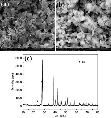 |
| | Fig. 6 SEM images and XRD pattern of the products obtained with different reaction temperatures: (a) 140 °C; (b) 220 °C; (c) 140 °C. | |
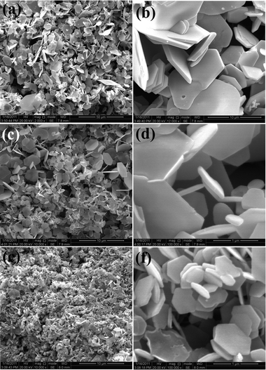
Solvent is also a very important factor for the synthesis of Sb2Te3 nanoplates. When less ethanediamine (2 mL) is involved in the reaction system, Te nanorods combined with a few Sb2Te3 nanoplates are obtained which can be seen in Fig. 7b. The XRD pattern also shows the existence of Te and Sb2Te3 (Fig. 7a). The reason why a few Sb2Te3 nanoplates can be synthesized under these conditions is the lack of OH− anions. In other words, in the weak alkali medium, the disproportionation from Te to Te2− and TeO32− ions is restrained. This phenomenon further proves the disproportionation reaction mechanism of the Te element in the solution. To determined the effect of pH value in the solution, the pH values before and after solvothermal treatment were measured, as shown in Table S1.† With a pH value of 10.8 (2 mL of ethanediamine), the disproportionation reaction can not proceed completely. Thus, Te and Sb2Te3 coexist. When 5 mL of ethanediamine is employed, the pH value of the solution increases (pH = 11.7), which accelerates the reaction greatly. As a result, the amount of Te is sharply reduced, meanwhile, the Sb2Te3 nanoplates increase (Fig. 7c). When the volume of ethanediamine reaches 10 mL (pH = 12.1), the disproportionation rate from Te to Te2− and TeO32− ions will be further increased. And the Te nanorods absolutely transform into irregular Sb2Te3 nanoplates, as can be seen in Fig. 7d. With a further increase in the volume of ethanediamine, some hexagonally shaped nanoplates with a wider size distribution are obtained at 15 mL of ethanediamine (Fig. 7e). If the volume ratio of ethanediamine to water increases to 20![[thin space (1/6-em)]](https://www.rsc.org/images/entities/char_2009.gif) :10, the reaction rate will be further accelerated, and uniform hexagonal nanoplates produced. As the volume ratio of ethanediamine to water continues to increase, the increasing reaction rate will lead to the uniform morphology and size distribution (Fig. 7f).
:10, the reaction rate will be further accelerated, and uniform hexagonal nanoplates produced. As the volume ratio of ethanediamine to water continues to increase, the increasing reaction rate will lead to the uniform morphology and size distribution (Fig. 7f).
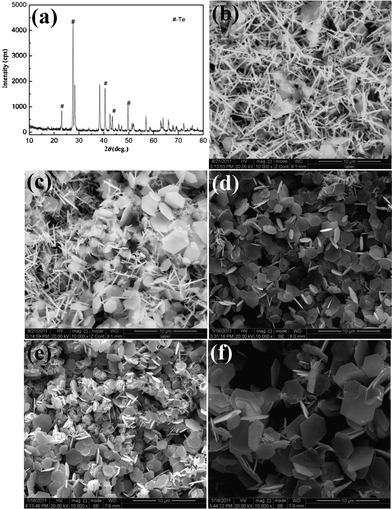 |
| | Fig. 7 The SEM images and XRD pattern of the prepared Sb2Te3 products after aging at 180 °C for 12 h in media with different volume ratios of ethanediamine and water: (a) 2:28; (b) 2:28; (c) 5:25; (d) 10:20; (e) 15:15; (f) 25:5. | |
Thermoelectrical transport properties
The four-probe electrical conductivity measurements in the temperature range of 300–600 K reveal that the three types of samples with different particle size have different electrical conductivities. The sample with the larger particle size has the highest electrical conductivity. The particle size influence on the electrical conductivity has been reported in the literature; it was demonstrated that electrical conductivity is lower for samples with smaller particle size and increases with increasing particle size because of the scattering of charge carriers by the increased density of grain boundaries for smaller grains.3,25 For all three types of samples, the electrical conductivity decreases with temperature, which are 59.1 S cm−1, 45.5 S cm−1, and 41.1 S cm−1 at room temperature and 30.1 S cm−1, 22.3 S cm−1, 21.4 S cm−1 at the temperature of 600 K for 500 nm, 60 nm and 40 nm particle samples, respectively (Fig. 8a). The measured electrical conductivity for all the three Sb2Te3 samples is two orders of magnitude lower than that of the corresponding bulk sample26 and exhibits strong size dependence. Moreover, the electrical conductivities of the three samples are lower than those of Sb2Te3 single crystalline nanowires26 and spark plasma sintering Sb2Te3 nanosheets,27 while higher than that of porous particle films with similar sizes.28 The possible explanation for the observed different electrical conductivity originates in the density of the pellets. The denser sample leads to the higher electrical conductivity. In order to determine the effect of the density, Archimedes principle is employed to measure the density of the sample, and the results are shown in Table S2.† The densities of the three samples have little difference, which further proves that the size of the products has much effect on the electrical conductivity rather than the density of the pellets. However, the density of the sample pressed in our work is possibly higher than that of porous films and lower than that prepared by spark plasma sintering process, hot pressed method or isostatic cool pressing technique. Thus, a higher value of electrical conductivity can be obtained in denser samples, e.g. hot pressed and spark plasma sintering pellets.
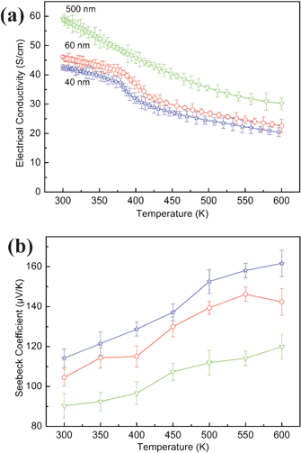 |
| | Fig. 8 (a) The electrical conductivities and (b) Seebeck coefficients of the obtained samples in the temperature range of 300–600 K. | |
Fig. 8b shows the Seebeck coefficients measured as a function of temperature for the three different sized Sb2Te3 samples. As can be seen, the Seebeck coefficients increase with increasing temperature for all the three samples, and they are affected by the variation in the particle size. Fig. 8b also demonstrates that all the three samples are p-type semiconductors with high maximum Seebeck coefficients about 119.9 μV K−1, 142.4 μV K−1, and 161.7 μV K−1 at 600 K for 500 nm, 60 nm and 40 nm particle samples. These values are higher than that of bulk Sb2Te3 crystals (79 μV K−1);28,29 but are lower than that of Sb2Te3 nanoparticles28 with the size of 20 nm and that of spark plasma sintering Sb2Te3 nanosheets.27 The enhanced Seebeck coefficient in smaller particles is thought to be possibly related to the energy filtering effect due to the charge carrier trapped in the grain boundaries regions,30,31 or to be connected with the increasing difference between the Fermi level and the average mobile carrier energy resulting from the quantum confinement effect.28,32
Conclusions
In summary, well-defined Sb2Te3 hexagonal nanoplates with a thickness of 40 nm were successfully prepared by a solvothermal treatment in the presence of glucose. Based on a series of contrast experimental results, a possible reaction process and formation mechanism of these hexagonal nanoplates have been proposed, which was related to self-assembly and an Ostwald ripening process. The glucose plays a crucial role in the formation process. The size and morphology of Sb2Te3 can be tuned by adjusting the concentration of the glucose. Moreover, the electrical conductivity and Seebeck coefficient were investigated as a function of temperature and thickness of the Sb2Te3 plate. The electrical conductivities are much smaller than the bulk value, while the Seebeck coefficients show much enhancement in smaller particle size.
Acknowledgements
This work is financially supported by the National Natural Science Foundation of China (Project no. 20871036, 21071036), Province Natural Science Foundation of Heilongjiang Province (ZD201011) and Scientific Research Innovation Foundation of Harbin Institute of Technology (Project no. GFCQ98332122).
References
- Y. N. Xia, P. D. Yang, Y. G. Sun, Y. Y. Wu, B. Mayers, B. Gates, Y. D. Yin, F. Kim and Y. Q. Yan, Adv. Mater., 2003, 15, 353–389 CrossRef CAS.
- H. Q. Liu, D. B. Kuang, A. W. Xu, Y. P. Fang, C. Frommen and D. Fenske, Adv. Mater., 2003, 15, 1747–1750 CrossRef CAS.
- M. S. Toprak, C. Stiewe, D. Platzek, S. Williams, L. Bertini, E. C. Muller, C. Gatti, Y. Zhang, M. Rowe and M. Muhammed, Adv. Funct. Mater., 2004, 14, 1189–1196 CrossRef CAS.
- J. S. Lee and U. A. Joshi, Small, 2005, 1, 1172–1176 CrossRef CAS.
- Z. H. Wang, L. Pan, H. B. Hu and S. P. Zhao, CrystEngComm, 2010, 12, 1899–1904 RSC.
- M. Sun, D. Z. Li, W. J. Zhang, X. Z. Fu, Y. Shao, W. J. Li, G. C. Xiao and Y. H. He, Nanotechnology, 2010, 21, 355601 Search PubMed.
- Y. Z. Jin, Y. F. Yang, H. P. He and Z. Z. Ye, CrystEngComm, 2010, 12, 2663–2665 RSC.
- P. O'Brien, S. S. Garje, D. J. Eisler, J. S. Ritch, M. Afzaal and T. Chivers, J. Am. Chem. Soc., 2006, 128, 3120–3121 CrossRef CAS.
- W. L. Suchanek, J. M. Garces, P. F. Fulvio and M. Jaroniec, Chem. Mater., 2010, 22, 6564–6574 CrossRef CAS.
- P. D. Yang, W. J. Liang, A. I. Hochbaum, M. Fardy, O. Rabin and M. J. Zhang, Nano Lett., 2009, 9, 1689–1693 CrossRef CAS.
- A. Majumdar, A. I. Hochbaum, R. K. Chen, R. D. Delgado, W. J. Liang, E. C. Garnett, M. Najarian and P. D. Yang, Nature, 2008, 451, 163-U165 Search PubMed.
- R. Venkatasubramanian, E. Siivola, T. Colpitts and B. O'Quinn, Nature, 2001, 413, 597–602 CrossRef CAS.
- J. H. Zhu, B. Zhou, Y. Ji, Y. F. Yang and X. H. Li, Cryst. Growth Des., 2008, 8, 4394–4397 CrossRef CAS.
- H. J. Zhang, W. D. Shi, L. Zhou, S. Y. Song and J. H. Yang, Adv. Mater., 2008, 20, 1892–1897 CrossRef CAS.
- W. Z. Wang, B. Poudel, J. Yang, D. Z. Wang and Z. F. Ren, J. Am. Chem. Soc., 2005, 127, 13792–13793 CrossRef CAS.
- Y. Cui, S. Meister, H. L. Peng, K. McIlwrath, K. Jarausch and X. F. Zhang, Nano Lett., 2006, 6, 1514–1517 CrossRef CAS.
- H. Park, J. S. Lee, S. Brittman and D. Yu, J. Am. Chem. Soc., 2008, 130, 6252–6258 CrossRef CAS.
- R. V. Devireddy, D. Pinisetty, M. Gupta, A. B. Karki and D. P. Young, J. Mater. Chem., 2011, 21, 4098–4107 RSC.
- D. L. W. Z. Wang, Y. J. Liang, G. L. Zhang, B. Q. Zeng and Q. Y. He, Langmuir, 2011, 27, 815–819 CrossRef CAS.
- H. J. Zhang, W. D. Shi, J. B. Yu and H. S. Wang, J. Am. Chem. Soc., 2006, 128, 16490–16491 CrossRef CAS.
- A. W. Xu, M. Antonietti, H. Colfen and Y. P. Fang, Adv. Funct. Mater., 2006, 16, 903–908 CrossRef CAS.
- W. D. Shi, L. Zhou, S. Y. Song, J. H. Yang and H. J. Zhang, Adv. Mater., 2008, 20, 1892–1897 CrossRef CAS.
- Z. L. Wang, W. G. Lu, Y. Ding, Y. X. Chen and J. Y. Fang, J. Am. Chem. Soc., 2005, 127, 10112–10116 CrossRef CAS.
- Z. Fang, X. Y. Wang, J. M. Shen, X. Lin, Y. H. Ni and X. W. Wei, Cryst. Growth Des., 2010, 10, 469–474 CAS.
- M. Takashiri, K. Miyazaki, S. Tanaka, J. Kurosaki, D. Nagai and H. Tsukamoto, J. Appl. Phys., 2008, 104, 084302 Search PubMed.
- P. Kim, Y. M. Zuev, J. S. Lee, C. Galloy and H. Park, Nano Lett., 2010, 10, 3037–3040 CrossRef CAS.
- Y. J. Zhu, G. H. Dong and L. D. Chen, J. Mater. Chem., 2010, 20, 1976–1981 RSC.
- Q. Y. Yan, J. Chen, T. Sun, D. Sim, H. Y. Peng, H. T. Wang, S. F. Fan, H. H. Hng, J. Ma, F. Y. C. Boey, S. Li, M. K. Samani, G. C. K. Chen, X. D. Chen and T. Wu, Chem. Mater., 2010, 22, 3086–3092 CrossRef CAS.
- C. Drasar, M. Steinhart, P. Lost'ak, H. K. Shin, J. S. Dyck and C. Uher, J. Solid State Chem., 2005, 178, 1301–1307 Search PubMed.
- J. Martin, L. Wang, L. Chen and G. S. Nolas, Phys. Rev. B, 2009, 79, 115311 CrossRef.
- T. C. Harman, D. L. Spears and M. J. Manfra, J. Electron. Mater., 1996, 25, 1121–1127 Search PubMed.
- D. V. Talapin, R. Y. Wang, J. P. Feser, J. S. Lee, R. Segalman and A. Majumdar, Nano Lett., 2008, 8, 2283–2288 CrossRef CAS.
Footnote |
| † Electronic supplementary information (ESI) available. See DOI: 10.1039/c1ra00642h |
|
| This journal is © The Royal Society of Chemistry 2012 |
Click here to see how this site uses Cookies. View our privacy policy here.