Electrospun conductive polyaniline–polylactic acid composite nanofibers as counter electrodes for rigid and flexible dye-sensitized solar cells†
Shengjie
Peng
*ab,
Peining
Zhu
c,
Yongzhi
Wu
d,
Subodh G.
Mhaisalkar
a and
Seeram
Ramakrishna
*ef
aSchool of Materials Science and Engineering, Nanyang Technological University, Singapore 639798
bNUS Nanoscience and Nanotechnology Initiative (NUSNNI)-NanoCore, National University of Singapore, Singapore 117576. E-mail: sjpeng@ntu.edu.sg
cDepartment ofMechanical Engineering, National University of Singapore, Singapore 117574
dNUS Graduate School for Integrative Sciences and Engineering, National University of Singapore, Singapore
eNational University of Singapore, Singapore 117576
fKing Saud University, 11451, Riyadh, Kingdom of Saudi Arabia. E-mail: seeram@nus.edu.sg
First published on 15th November 2011
Abstract
Conductive polyaniline doped with 10-camphorsulfonic acid (PANI·CSA) blended with polylactic acid (PLA) composite films are directly deposited on rigid fluorine-doped tin oxide and flexible indium tin oxide-coated polyethylene naphthalate substrates by using a simple electrospinning method. The scanning electron microscope and atomic force microscope images show that the PANI·CSA–PLA film is assembled from about 200 nm-diameter nanofibers, with a generally uniform thickness of about 2 μm. The three-dimensional porous fibrous PANI·CSA–PLA films indicate good electrocatalytic performance for I3−/I− electrolyte, demonstrated by electrochemical impedance spectra and cyclic voltammetry measurements. The photoelectric conversion efficiency of the dye-sensitized solar cells (DSCs) firstly based on such rigid and flexible PANI·CSA–PLA counter electrodes achieves 5.3% and 3.1% under 1 sun illumination of 100 mW cm−2 (AM 1.5), respectively, which is close to that of sputtered Pt-based DSCs. In addition, the rigid PANI·CSA–PLA-based DSC demonstrates good stability. As the PANI·CSA–PLA counter electrodes can be obtained in a short time at room temperature, they are potentially applicable in large-area DSCs and suitable for flexible DSCs.
Introduction
Dye-sensitized solar cells (DSCs), as a potential alternative to silicon-based solar cells, have received a lot of interest over the last decades due to their low cost, high efficiency and simple preparation process.1 The counter electrodes of DSCs, which can collect electrons and catalyze the redox couple regeneration, are usually constructed by noble metal Pt films. Although the Pt-based DSCs achieve good performance, the most common fabrication methods of Pt films such as thermal decomposition and vacuum sputtering normally need high temperature operation and complex facilities, which limit their application in flexible DSCs and the production on a large scale.2–4 In addition, the high price and scarce resource of Pt are serious drawbacks in cost-effective fabrication of solar cells. Therefore, cheap counter electrodes with high catalytic performance and facile fabrication procedures are required for the commercial application of DSCs. Some carbonaceous materials, nitride and sulfide compounds have been employed as counter electrodes in efficient DSCs.5–8Recently, conductive polymers have been widely investigated as promising candidates for the counter electrode materials due to their unique properties, such as high conductivity, good stability, low cost and good catalytic activity for I3−reduction.9–11 Among various conductive polymers, conductive polyaniline (PANI) is one of the most studied conductive polymers because of its easy synthesis, high conductivity, and interesting redox catalytic properties. Therefore, researchers have fabricated conductive PANI counter electrodes by electrodeposition and dip-coating methods for efficient DSCs.12,13 It is known that electrospinning is a simple and versatile method of electrostatically induced top to bottom approach of nanofabrication process. The electrospinning technique has advantages over other methods, including the easy formation of films directly on substrates, low cost and easy process, which can make the technique suitable for large-scale production of nanostructures economically.14,15 Therefore, the electrospun conductive polymers can be used as counter electrode materials for efficient DSCs.
In this paper, a simple electrospinning method is developed to directly deposit conductive 10-camphorsulfonic acid (CSA)-doped polyaniline (PANI) blended with polylactic acid (PLA) composite films (PANI·CSA–PLA) on rigid fluorine-doped tin oxide (FTO) and flexible indium tin oxide-coated polyethylene naphthalate (PEN) substrates. The rigid and flexible DSCs demonstrate high photovoltaic efficiency, close to that of sputtered Pt-based DSCs. The stability of the rigid DSC is also promising. The present preparation process of PANI·CSA–PLA counter electrodes is simple and cost-efficient, and thus feasible for the large-scale and flexible application of DSCs.
Experimental
Materials
Polyaniline emeraldine (PANI, Mw = 65![[thin space (1/6-em)]](https://www.rsc.org/images/entities/char_2009.gif) 000), 10-camphorsulfonic acid (CSA), polylactic acid (PLA, Mw = 300000), TiCl4 and chloroform were purchased from Sigma-Aldrich. FTO (10 Ω sq−1) and PEN substrates (20 Ω sq−1) were purchased from Asahi Glass Co. Ltd., Japan. Two kinds of TiO2 pastes for low temperature and high temperature heat treatment processes were purchased from Solaronix. All these materials were used as received without any further purification.
000), 10-camphorsulfonic acid (CSA), polylactic acid (PLA, Mw = 300000), TiCl4 and chloroform were purchased from Sigma-Aldrich. FTO (10 Ω sq−1) and PEN substrates (20 Ω sq−1) were purchased from Asahi Glass Co. Ltd., Japan. Two kinds of TiO2 pastes for low temperature and high temperature heat treatment processes were purchased from Solaronix. All these materials were used as received without any further purification.
Fabrication of PANI·CSA–PLA, PANI–PLA, and Pt counter electrodes
PANI·CSA–PLA and PANI–PLA composite films were fabricated by a simple electrospinning technology. In a typical synthesis of PANI·CSA–PLA film, an electrospinning solution was made by thoroughly mixing 0.05 g of PANI, 0.065 g of CSA 0.12 g of PLA and 2 mL of chloroform under vigorous stirring and then loaded into a plastic syringe. The obtained structural formula of PANI·CSA is shown in Fig. 1. Then the obtained green solution was electrospun at a rate of 1.0 mL h−1 and an electric field of 25 kV. FTO or PEN substrates were placed onto an aluminum collector to collect nanofiber films. The electrospinnig time was about 3 min. The thickness of the film could be controlled by the electrospinning time. Moreover, the PANI-PLA nanofiber film was fabricated by electrospinning a solution containing 0.05 g of PANI, 0.12 g of PLA and 2 mL of chloroform, and the electrospinning parameters were similar to those of the electrospun PANI·CSA–PLA nanofibers. For comparison, Pt films on FTO and PEN substrates were obtained by sputtering.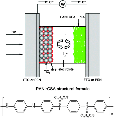 | ||
| Fig. 1 Schematic diagram of the cross-sectional image for the DSC based on PANI·CSA-PLA nanofiber film on FTO or PEN substrates as the counter electrode and the structural formula of the conductive PANI·CSA. | ||
Fabrication of TiO2 electrodes
Cleaned FTO glass substrates were first treated with 50 mM of TiCl4 aqueous solution at 70 °C for 30 min. The TiO2 films with a thickness of about 15 μm were prepared by screen printing commercial TiO2 paste onto the TiCl4-treated FTO substrates for several times. Then the films were dried in air at 80 °C for 30 min and calcined at 450 °C for 30 min. The heated TiO2 electrodes were treated by 50 mM of TiO2 at 70 °C for 30 min and then recalcined at 450 °C for 30 min and cooled down to 80 °C. Finally, the TiO2 electrodes were soaked in a dry N719 methanol solution for 24 h.16,17 When referred to flexible TiO2 electrodes, the TiO2 films were printed on PEN substrates by using binder-free TiO2 paste and then heated at 120 °C for 1 h. The fabrication procedure of flexible PEN-based TiO2 electrodes was similar to that of the rigid FTO-based TiO2 electrodes.Assembly of DSCs
DSCs were assembled by filling the electrolyte solution (a mixture of 0.6 M DMPImI, 0.1 M LiI, 0.05 M I2, and acetonitrile solvent) between the N719 dye sensitizer anchored TiO2 films and the counter electrodes, as shown in Fig. 1. The active area of the DSCs is 0.16 cm2.Characterization and measurements
The morphology of the as-obtained films was investigated by using scanning electron microscopy (SEM, JEOL JSM-6701F), operated at 10 kV. Atomic force microscopy (AFM) characterization of the PANI·CSA–PLA composite films was carried out by using a Nanoscope III (Digital Instruments, Inc., Santa Barbara, CA, USA) in tapping mode in air. Infrared (IR) spectra of the composite films were performed on Fourier transformed infrared spectrometer (FTS-3500ARX). Electrochemical impedance spectroscopy (EIS) spectra of the films were investigated by a PARSTAT 2273 electrochemical analyzer to determine the catalytic effect of the PANI–PLA, PANI·CSA–PLA, or Pt film in a symmetric cell. EIS spectra were obtained at zero bias potential and 10 mV amplitude over the frequency range 0.01–105 Hz.18Cyclic voltammetry (CV) of the PANI-PLA, PANI·CSA–PLA, or Pt film was carried out in N2-purged acetonitrile solution at a scan rate of 50 mV s−1. The as-prepared film, a Pt coil, and an Ag+/Ag electrode were used as the working electrode, the counter electrode, and the reference electrode, respectively. The electrolyte was the acetonitrile solution containing 0.1 M LiClO4 as the supporting electrolyte and 10 mM LiI + 1 mM I2 as the redox couple. Photocurrent density–voltage curves were obtained by using a potentiostat (Autolab PGSTAT30, Eco Chemie B.V., The Netherlands). Photocurrent measurements were performed under 1 sun illumination of 100 mW cm−2xenon lamp (Thermo Oriel Xenon Lamp 150 W: Model 66902) with AM 1.5G condition. Incident photon-to-current conversion efficiency (IPCE) measurements were done using the standard kit from Oriel Instruments (model QE-PV-SI, Silicon detector, Newport Corporation, US).Results and discussion
Fig. 2a–d display SEM images of the as-electrospun PANI–PLA and PANI·CSA–PLA films on FTO substrates. It can be seen that the substrates are fully covered by non-woven nanofiber mats. The average diameter of PANI·CSA–PLA nanofiber determined from the SEM images is about 200 nm, with a standard deviation of about 100 nm and length up to several hundred micrometres (Fig. 2b,c), which is similar to that of PANI–PLA nanofibers (Fig. 2a). The as-electrospun PANI·CSA–PLA nanofibers are stacked and bonded with the substrate firmly, resulting in an interconnected nanofibrous network with a thickness of about 2 μm (Fig. 2d). This network structure is in favor of the infiltration of electrolyte and further promotes the electrocatalytic activity for the reduction of I3−. It should be noted that no fibers formed without the addition of PLA into the PANI·CSA solution, as the viscosity and surface tension of the solution were not high enough to form nanofibers during electrospinnig.19 After doping with CSA, the color of the polymer films changed from blue to green, indicating its electrical conductivity characteristics from non-conductivity (Fig. 2e,f). Fig. 2g shows that the PANI·CSA–PLA nanofiber film based on the PEN substrate exhibits higher adhesion against mechanical scratching and bending.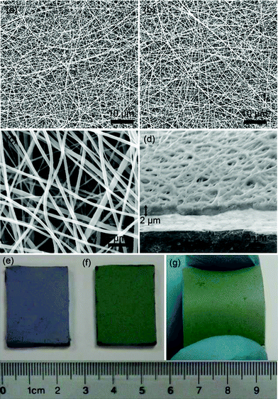 | ||
| Fig. 2 SEM images of the top views (a and b) of the PANI-PLA and PANI·CSA-PLA film on FTO glass, the magnified part (c) and cross-sectional view (d) of the PANI·CSA–PLA nanofiber film, and the photos of the PANI-PLA/FTO (e), PANI·CSA–PLA/FTO (f), and PANI·CSA–PLA/PEN (g), respectively. | ||
In order to better observe the surface topography of the PANI·CSA–PLA nanofiber film, AFM experiments were also carried out on the deposited nanofiber mat. Fig. 3a,b show 2D and 3D AFM images of PANI·CSA–PLA composite nanofibers, respectively. These nanofibers possess a diameter of about 100–300 nm as found in the SEM images. It can be seen that many nanofibers randomly orient to form a three-dimensional porous fibrous web, due to the effects of drawing and high-shear flow during electrospinning. This morphological feature can make PANI·CSA–PLA composite film take up much electrolyte and further catalyze I3−reduction, which can be ascribed to the higher specific surface area, higher porosity, and unique tortuosity of the pore structure.20,21
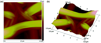 | ||
| Fig. 3 2D and 3D AFM images of the PANI·CSA–PLA composite film. | ||
Fig. 4 displays IR spectra of the PANI–PLA and PANI·CSA–PLA composite films. The peak assignments for PANI–PLA and PANI·CSA–PLA composite films are shown in Table S1 (ESI†). The absorption bands at 1588 cm−1 and 1480 cm−1 are assigned to the C![[double bond, length as m-dash]](https://www.rsc.org/images/entities/char_e001.gif) C stretching of the quinoid and benzenoid rings of PANI, respectively.22 The peaks at 1751 cm−1, 1455 cm−1, and 866 cm−1 are assigned at C–O, –CH3, and C–H bands of PLA, respectively.23 After doping with CSA, some new characteristic peaks are observed. They are 1475 cm−1, 1092 cm−1, and 590 cm−1. The characteristic bands of CSA-doped PANI appear at 1092 cm−1 and 1475 cm−1. The location of such new peaks is similar to the literature, which may be an interaction between polyaniline and the dopant CSA.24 Apart from the new peaks, some peaks of the PANI–PLA such as 1588 cm−1 and 1480 cm−1 are missing. The reason is probably because of the attachment of the dopant to the nitrogen atom of the PANI, and the deformation process of the rings is hindered.
C stretching of the quinoid and benzenoid rings of PANI, respectively.22 The peaks at 1751 cm−1, 1455 cm−1, and 866 cm−1 are assigned at C–O, –CH3, and C–H bands of PLA, respectively.23 After doping with CSA, some new characteristic peaks are observed. They are 1475 cm−1, 1092 cm−1, and 590 cm−1. The characteristic bands of CSA-doped PANI appear at 1092 cm−1 and 1475 cm−1. The location of such new peaks is similar to the literature, which may be an interaction between polyaniline and the dopant CSA.24 Apart from the new peaks, some peaks of the PANI–PLA such as 1588 cm−1 and 1480 cm−1 are missing. The reason is probably because of the attachment of the dopant to the nitrogen atom of the PANI, and the deformation process of the rings is hindered.
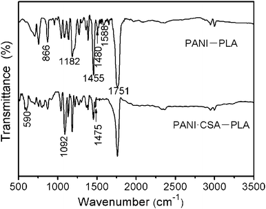 | ||
| Fig. 4 IR spectra of the PANI–PLA and PANI·CSA–PLA composite films, respectively. | ||
Fig. 5 shows the Nyquist plots, and Bode plots of the symmetrical PANI–PLA film, PANI·CSA–PLA film and sputtered Pt film on FTO substrates. It can be seen that each Nyquist plot contains three distinguishable impedances, which are assigned in the order of decreasing frequency to, ohmic serial resistance (Rs), charge transfer resistance (Rct) and Nernst diffusion impedance (Zw).25 The Rct represents the electron transfer to and from the triiodide, which can be taken as half of value of the real component. The smaller the semicircle is, the better the catalytic performance is. Table 1 shows the electrical conductivity and EIS parameters of the symmetrical cells with PANI–PLA/FTO, PANI·CSA–PLA/FTO and Pt/FTO electrodes. When the PANI–PLA film was deposited on the FTO substrate, the Rct is deduced to be 10.6 Ω cm2 from the equivalent circuit (Fig. 5b). After doping with CSA, it can be found that the Rs, Rct and Zw of the PANI·CSA–PLA film is decreased, compared with that of PANI–PLA film. The lower Rs of PANI·CSA–PLA film is attributed to the higher electrical conductivity, compared with PANI–PLA film. The Rct of PANI·CSA–PLA film is reduced to 2.4 Ω cm2, demonstrating good catalytic performance for I3−reduction. This Rct value of PANI–PLA film is comparable to that of the Pt film (2.1 Ω cm2), indicating an ideal counter electrode material for DSCs. For a good performance of the DSCs, it should be < 10 Ω cm2.25 Furthermore, in the imaginary impedance plot (Fig. 5b), it is found that the characteristic peak value of PANI·CSA–PLA in high-frequency regime (103–105 Hz), corresponding to the electron transfer at the counter electrode–electrolyte interface, shifts to a higher frequency compared with PANI–PLA, suggesting the increased rate of redox reaction of I3−/I− and a faster electron transfer at the interface between PANI·CSA–PLA and electrolyte.26 This result reveals that the catalytic performance of the PANI·CSA–PLA film is higher than that of the PANI–PLA film, which is ascribed to the contribution of the high surface area of PANI·CSA–PLA nanofibers and relatively high electrical conductivity of PANI·CSA–PLA film.
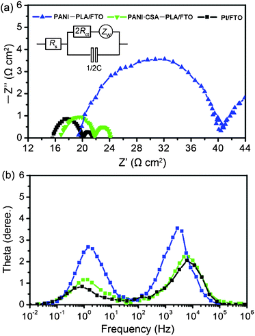 | ||
| Fig. 5 Nyquist plots (a), and Bode plots (b) of the symmetrical PANI–PLA, PANI·CSA-PLA and sputtered Pt films on FTO substrates. The inset is the equivalent circuit for the impedance spectrum. Zw: Nernst diffusion impedance; Rct: charge transfer resistance of one electrode; C: double layer capacity of one electrode; Rs: serial resistance. | ||
| Electrodes | Conductivity (S cm−1) | R s (Ω cm2) | R ct (Ω cm2) | Z w (Ω cm2) |
|---|---|---|---|---|
| PANI–PLA/FTO | 1.5 × 10⁻⁵ | 19.5 | 10.6 | 10.5 |
| PANI·CSA–PLA/FTO | 8.4 × 10⁻² | 16.7 | 2.4 | 1.2 |
| Pt/FTO | 2.1 × 10³ | 15.5 | 2.1 | 0.91 |
In addition, the fitted result shows that the Zw of PANI·CSA–PLA is lower than that of PANI–PLA, which may be caused by the more catalytic sites of PANI·CSA–PLA nanofibers and a higher electrical conductivity. This result means that triiodide ions can be rapidly reduced to iodide ions under catalysis of PANI·CSA–PLA nanofibers, and this can accelerate diffusion of triiodide ions. However, the Zw of PANI·CSA–PLA is larger than that of Pt, which may be caused by the thicker PANI·CSA–PLA nanofiber film than the Pt film.27 Undeniably, the PANI·CSA–PLA electrode demonstrates a comparable Rct and a larger Zw, compared to those of Pt electrode. The larger Zw may be the main reason for the relatively low photovoltaic performance of the DSCs based on the PANI·CSA–PLA electrode.
Fig. 6 shows the cyclic voltammograms of the PANI–PLA, PANI·CSA–PLA, Pt electrodes, which were carried out in the acetonitrile solution containing 0.1 M LiClO4 as the supporting electrolyte and 10 mM LiI, 1 mM I2 as the redox couple, and Pt foil as working electrode. Two redox couples are observed. The anodic peak obtained from the CV curves corresponds to the oxidation of iodide to triiodide and the cathodic peak corresponds to the reduction of triiodide.28
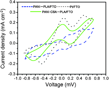 | ||
| Fig. 6 CV of the PANI–PLA, PANI·CSA–PLA and Pt films on FTO glass substrates. | ||
It is observed that the oxidation and reduction peaks of the PANI·CSA–PLA film are a little lower than those of the Pt electrode, which indicates the possibility of electrocatalytic behavior for the I3−reduction on the PANI·CSA–PLA nanofiber film. As the PANI–PLA film possesses a lower current density, it has a poor catalytic performance compared to that of PANI·CSA–PLA and Pt electrodes.29 This result coincides with the charge transfer resistance Rct obtained from the EIS measurement.
Fig. 7 shows the photocurrent density–voltage (J–V) curves of the DSCs with FTO glass, PANI-PLA/FTO, PANI·CSA–PLA/FTO, Pt/FTO, PANI·CSA–PLA/PEN, and Pt/PEN counter electrodes, respectively. Table 2 summarizes the photoelectric parameters of DSCs such as Voc: open-circuit voltage; Jsc: short-circuit current density; FF: fill factor; η: energy conversion efficiency. Under 1 sun illumination of 100 mW cm−2 (AM 1.5), the DSC with the PANI·CSA–PLA film on FTO glass as the counter electrode exhibits a reasonable high photoelectrical conversion efficiency of 5.30%, which is comparable to that of the Pt-based device (6.51%) and much higher than a PANI–PLA-based DSC (1.6%). When the counter electrode is FTO, the conversion efficiency is very low, confirming that the catalytic effect originates mainly from PANI·CSA–PLA nanofiber film. It is observed that the PANI·CSA-PLA electrode shows a similar Voc value to that of the Pt electrode, whilst a little lower Jsc and FF. In DSCs, the FF is determined by the total series resistance (RStot) of the DSC device, which can be expressed as RStot = Rs + Rct + Rd. The increase of the Rs and Rd leads to an increase of RStot and the corresponding reduction in the FF.30,31 Also, the RStot in turn partly influences the Jsc according to the equation Jsc = Voc/RStot + constant.32 The higher RStot can limit the photocurrent density. Furthermore, it is found that the IPCE of the PANI·CSA–PLA-based cells was slightly smaller than that of the Pt based devices in the 400–750 nm spectral range, which is consistent with the relatively low Jsc (Fig. S1, ESI†). As the RStot of PANI·CSA–PLA film with higher electrical conductivity is much lower than that of PANI–PLA film, this results in much higher conversion efficiency of PANI·CSA–PLA-based DSC than that of PANI–PLA-based DSC. Although the efficiency of the PANI·CSA–PLA-based DSC is a little lower than that of the Pt-based DSC, the small decrease of the efficiency is acceptable, because the raw materials for PANI·CSA–PLA is low cost and can decrease the cost of Pt-based DSCs for large-scale application. As the PANI·CSA–PLA film can be electrospun on substrates under room temperature, it can be directly used as the counter electrode in flexible DSC. This means that the counter electrode can be obtained by electrospinning PANI·CSA–PLA film directly on the PEN substrate. It is found that the flexible DSC based on the PANI·CSA–PLA counter electrode can exhibit a conversion efficiency of 3.1%. Although this result is a little lower than that of the sputtered Pt-based flexible DSC (4.39%), it provides a potential plastic counter electrode material for flexible DSCs.
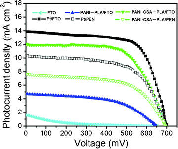 | ||
| Fig. 7 Photocurrent density–voltage (J–V) curves of DSCs based on FTO glass, PANI–PLA/FTO, PANI·CSA–PLA/FTO, Pt/FTO, PANI·CSA–PLA/PEN, and Pt/PEN counter electrodes respectively, under 1 sun illumination of 100 mW cm−2 (AM 1.5). | ||
In addition, the PANI·CSA–PLA/FTO-based DSC shows good stability, which was tested in dark under room temperature (Fig. 8). During the test, the open voltage Voc moderately increases a little while the Jsc and FF both decreases a little. The total energy conversion efficiency achieves 4.77% and retains 90% of its initial value after 25 days. The well demonstrated stability indicates that the PANI·CSA–PLA films are promising counter electrode candidates for efficient DSCs.
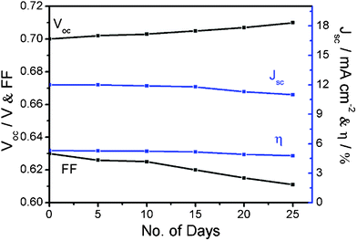 | ||
| Fig. 8 A short-term evaluation of the stability of the J–V parameters of the DSC with PANI·CSA–PLA/FTO as the counter electrode, under 1 sun illumination of 100 mW cm−2 (AM 1.5). | ||
Conclusions
In conclusion, electrospun conductive PANI·CSA–PLA nanofiber films have been employed as counter electrodes for efficient DSCs, which showed reasonably good photoelectrical conversion efficiency, achieving 82% performance level of the sputtered Pt electrode. Furthermore, as the electrospun PANI·CSA–PLA films on different substrates (FTO and PEN) can be obtained in a short time and the production steps are carried out under ambient temperature, these counter electrodes are potentially very cost-effective and suitable for reel-to-reel synthesis.Acknowledgements
This work was supported by Singapore NRF-CRP grant on “Nanonets for harnessing solar energy and storage” and also NUS and NTU for providing facilities to carry out the research.References
- M. K. Nazeeruddin, F. D. Angelis, S. Fantacci, A. Selloni, G. Viscardi, P. Liska, S. Ito, B. Takeru and M. Grätzel, J. Am. Chem. Soc., 2005, 127, 16835–16847 CrossRef CAS.
- N. Papageorgiou, W. F. Maier and M. Grätzel, J. Electrochem. Soc., 1997, 144, 876–884 CAS.
- Y. L. Lee, C. L. Chen, L. W. Chong, C. H. Chen, Y. F. Liu and C. F. Chi, Electrochem. Commun., 2010, 12, 662–1665 Search PubMed.
- X. Yin, Z. S. Xue and B. Liu, J. Power Sources, 2011, 196, 2422–2426 Search PubMed.
- J. D. Roy-Mayhew, D. J. Bozym, C. Punckt and I. A. Aksay, ACS Nano, 2010, 4, 6203–6211 CrossRef.
- G. R. Li, F. Wang, Q. W. Jiang, X. P. Gao and P. W. Shen, Angew. Chem. Int. Ed., 2010, 49, 3653–3656 CAS.
- M. Wang, A. M. Anghel, B. Marsan, N. L. C. Ha, N. Pootrakulchote, S. M. Zakeeruddin and M. Grätzel, J. Am. Chem. Soc., 2009, 131, 15976–15977 CrossRef CAS.
- Y. Hu, Z. Zheng, H. M. Jia, Y. W. Tang and L. Z. Zhang, J. Phys. Chem. C, 2008, 112, 13037–13042 CrossRef CAS.
- J. M. Pringle, V. Armel and D. R. MacFarlane, Chem. Commun., 2010, 46, 5367–5369 RSC.
- S. Ameen, M. S. Akhtar, Y. S. Kim, O. B. Yang and H. S. Shin, J. Phys. Chem. C, 2010, 114, 4760–4764 CrossRef CAS.
- H. Nagaia and H. Segawa, Chem. Commun., 2004, 974–975 RSC.
- J. Zhanga, T. Hreida, X. X. Li, W. Guo, L. P. Wang, X. T. Shi, H. Q. Sua and Z. B. Yuan, Electrochim. Acta, 2010, 55, 3664–3668 CrossRef CAS.
- Q. H. Li, J. H. Wu, Q. W. Tang, Z. Lan, P. J. Li, J. M. Lin and L. Q. Fan, Electrochem. Commun., 2008, 10, 1299–1302 CrossRef CAS.
- Z. M. Huang, Y. Z. Zhang, M. Kotaki and S. Ramakrishna, Compos. Sci. Technol., 2003, 63, 2223–2253 CrossRef CAS.
- W. E. Teo and S. Ramakrishna, Nanotechnology, 2006, 17, R89–R106 CrossRef CAS.
- F. S. Cai, J. Liang, Z. L. Tao, J. Chen and R. S. Xu, J. Power Sources, 2008, 177, 631–636 Search PubMed.
- S. J. Peng, J. F. Shi, J. Pei, Y. L. Liang, F. Y. Cheng, J. Liang and J. Chen, Nano Res., 2009, 2, 484–492 Search PubMed.
- S. J. Peng, F. Y. Cheng, J. F. Shi, J. Liang, Z. L. Tao and J. Chen, Solid State Sci., 2009, 11, 2051–2055 Search PubMed.
- I. D. Norris, M. M. Shaker, F. K. Ko and A. G. MacDiarmid, Synth. Met., 2000, 114, 109–114 CrossRef CAS.
- J. U. Kim, S. H. Park, H. J. Choi, W. K. Lee, J. K. Lee and M. R. Kim, Sol. Energy Mater. Sol. Cells, 2009, 93, 803–807 CrossRef CAS.
- Y. H. Ding, W. Di, Y. Jiang, F. Xu, Z. L. Long, F. M. Ren and P. Zhang, Ionics, 2009, 15, 731–734 Search PubMed.
- Y. M. Lee, S. Y. Ha, Y. K. Lee, D. H. Suh and S. Y. Hong, Ind. Eng. Chem. Res., 1999, 38, 1917–1924 Search PubMed.
- J. J. Guan and M. A. Hanna, Ind. Eng. Chem. Res., 2005, 44, 3106–3115 CrossRef CAS.
- T. Jana and A. K. Nandi, Langmuir, 2000, 16, 3141–3147 CrossRef CAS.
- A. Hauch and A. Georg, Electrochim. Acta, 2001, 46, 3457–3466 CrossRef CAS.
- M. X. Wu, X. Lin, A. Hagfeldt and T. L. Ma, Chem. Commun., 2011, 47, 4535–4537 RSC.
- D. W. Zhang, X. D. Li, S. Chen, F. Tao, Z. Sun, X. J. Yin and S. M. Huang, J. Solid State Electrochem., 2010, 14, 1541–1546 CrossRef CAS.
- J. H. Wu, Q. H. Li, L. Q. Fan, Z. Lan, P. J. Li, J. M. Lin and S. C. Hao, J. Power Sources, 2008, 181, 172–176 CrossRef CAS.
- K. M. Lee, P. Y. Chen, C. Y. Hsu, J. H. Huang, W. H. Ho, H. C. Chen and K. C. Ho, J. Power Sources, 2009, 188, 313–318 CrossRef CAS.
- P. Joshi, Y. Xie, M. Ropp, D. Galipeau, S. Bailey and Q. Q. Qiao, Energy Environ. Sci., 2009, 2, 426–429 RSC.
- R. R. Jia, J. Z. Chen, J. H. Zhao, J. F. Zheng, C. Song, L. Li and Z. P. Zhu, J. Mater. Chem., 2010, 20, 10829–10834 RSC.
- J. Han, H. Kim, D. Y. Kim, S. M. Jo and S. Y. Jang, ACS Nano, 2010, 4, 3503–3509 CrossRef CAS.
Footnote |
| † Electronic supplementary information (ESI) available: Band Assignments of PANI–PLA and PANI·CSA–PLA composite films, and IPCE curves of the DSCs fabricated with PANI–PLA, PANI·CSA–PLA, and Pt counter electrodes. See DOI: 10.1039/c1ra00618e |
| This journal is © The Royal Society of Chemistry 2012 |