Solvent spray method for simple fabrication of surface nanostructures of molecular thin films
J.
Kim
,
C. R.
Park
and
S.
Yim
*
Department of Chemistry, Kookmin University, Seoul, 136-702, South Korea. E-mail: sgyim@kookmin.ac.kr; Fax: +82-2-910-4415; Tel: +82-2-910-4734
First published on 24th November 2011
Abstract
In this work, zinc phthalocyanine (ZnPc) nanorods with various aspect ratios were effectively fabricated by spraying acetone/water mixed solvents onto the surface of ZnPc thin films. The lengths of the nanorods formed varied with the composition of the solvents used. The electronic absorption band of the film was broadened by the treatment, but it was almost completely recovered by post-annealing the film at 200 °C. This spray method is very simple compared to conventional surface nanostructuring technologies such as nanoimprinting and applicable to most organic films since the amount and composition of the solvents used are easily controllable.
1. Introduction
Control over surface morphology of organic thin films is of considerable interest since it is widely recognized that the performance of organic (opto)electronic devices is highly dependent on the morphology of the interface between organic layers.1–3 Especially in organic photovoltaic (OPV) cells, a controlled nanostructure with a large contact area between the electron donating and accepting layers is necessary to improve the power conversion efficiency (PCE) of the cells.4–6 This is because the short exciton diffusion lengths in organic semiconductors with respect to the film thickness limit the charge (hole and electron) separation before exciton recombination. The bulk heterojunction (BHJ) induced by co-deposition or homogeneous blend was initially introduced to achieve a large donor–acceptor interface.7,8 This interpenetrating network led to an increase in the PCE of the cells to some extent, but the charge trapping at bottlenecks and cul-de-sacs induced by the random distribution of donor and acceptor materials hampered further increases in efficiency.9,10 In this context, a heterolayer structure with an interdigitated morphology has been proposed to be an ideal interface.11,12 To fabricate a periodically nanostructured morphology, imprinting technologies using various templates such as a surface-directed demixing template,13 nematic gel template,14 and silicon templates patterned using a block copolymer15 have been applied. These techniques, however, require long and complicated nano-processes for the fabrication of the templates. To address this limitation, several simpler methods for surface nanostructuring have been introduced. Especially for porphyrinoid dyes such as phthalocyanines (Pcs), various methods for nano-crystalline film fabrications including the usage of solvent mixtures and their energetic and light harvesting properties were well reviewed previously.16,17 More recently, Xi. et al.18 reported that dropping and evaporation of various organic solvents onto and from the CuPc thin films resulted in surface nanorods with widths of 40–60 nm and lengths of 200–400 nm. Although this treatment is simple and does not require additional nano-processes, it cannot be readily applied to other organic thin films since during the treatment the film surface is entirely covered with the solvents, i.e. the method can be applied to only films having extremely low solubility in organic solvents.In this work, we developed an alternative simple solvent spray method, which can be utilized as a more general way to fabricate surface nanostructures of organic thin films. This method is expected to be applicable to most organic films since the amount of treating solvents is easily controllable. Here, we subjected the surfaces of zinc phthalocyanine (ZnPc) thin films to the solvent spray treatment using solvent mixtures of varying amounts and compositions. The related change of surface morphology, i.e. the formation of nanorods with various dimensions, and electronic absorption property of the films were observed. The effect of post-annealing on spray-treated films was also investigated.
2. Experimental
ZnPc thin films were grown in an ultrahigh vacuum organic molecular beam deposition (OMBD) chamber with a base pressure of ∼2 × 10⁻⁸ torr. Commercially available ZnPc (Aldrich Chemical, 97%) powder was purified twice using temperature gradient sublimation. The purified material was then outgassed in the vacuum chamber for 15–20 h before growth and then sublimed from a miniature effusion cell onto well cleaned glass substrates held at room temperature. The aperture of the efficient cell was ∼8 mm and the pressure in the chamber was maintained at 5 × 10⁻⁸–1 × 10⁻⁷ torr. during the deposition. The cell temperature was 370 °C, which corresponded to a growth rate of ∼0.3 Å s−1 as determined using a quartz crystal microbalance (QCM) positioned near the substrate.For the solvent spray treatment, the film was positioned on a Petri dish and various solvents were sprayed onto the surface of the film. Fig. 1 shows a schematic diagram of the solvent spray system used for treatment. A spray nozzle (1/4JNSS, Spraying Systems Co.) system contained two supply routes and valves for solvent mixture and N2 flow gas, which can easily control the amount of solvents. The distance between the sample and the nozzle was maintained at 20 cm, which corresponded to a spray rate of 30 ml m−2 s. After the spray treatment, solvents were volatilized for 12 h at room temperature under N2 atmosphere. The surface morphology of the samples was analyzed using a field emission scanning electron microscope (FE-SEM) (JEOL JSM 740F) and atomic force microscope (AFM) (SII SPA 400), and the electronic absorption of the films was recorded using an ultraviolet(UV)-visible spectrophotometer (Scinco S-3100).
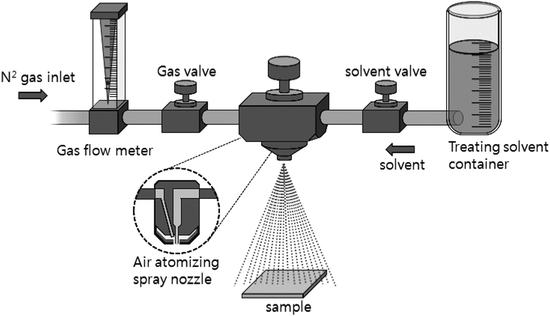 | ||
| Fig. 1 Schematic diagram of the solvent-spray system used in this study. | ||
3. Results and discussion
ZnPc is a prospective electron donor material for OPV cells due to its favorable physical properties such as thermal and chemical stability, wide absorption band in the visible region, and high hole mobility.19ZnPc thin films with a thickness of 50 nm were grown on glass substrates using organic molecular beam deposition (OMBD). The film was flat and characterized by fine grains as shown in Fig. 2(a) and 3(a), which is characteristic of α-ZnPc films.20Acetone/water mixed solvents at various concentration ratios were then sprayed onto the film surface for one second. After the spray treatment, the samples were dried at room temperature for 12 h and changes in surface morphologies were observed. Fig. 2(b)–2(f) show representative FE-SEM images of the solvent spray treated surfaces of ZnPc thin films. As shown in these figures, bundles of nanorods with various lengths and widths were observed. When the as-deposited film was treated with acetone/water (50![[thin space (1/6-em)]](https://www.rsc.org/images/entities/char_2009.gif) :50 vol%) spray, the average width and length of the nanorods were ∼40.7 nm and ∼62.5 nm, respectively (Fig. 2b). As the acetone concentration increased, the lengths of the nanorods tended to increase, while the widths did not change appreciably. For example, in the case that the film treated with acetone/water (94:6 vol%) spray, the nanorods with an average width of ∼41.6 nm and length of ∼250 nm were obtained (Fig. 2e). When the film was sprayed with 100% acetone, the observed width and length of the nanorods were ∼35.4 nm and ∼288 nm, respectively (Fig. 2f). The gradual increase in the lengths of nanorods as the water content decreased indicates that the extremely low water solubility of ZnPc prevented the dissolution of ZnPc in the mixed solvent and consequently retarded the elongation of the nanorods. The acetone-100% spray treatment changed the orientation of the nanorods as well as the dimension. For the acetone/water mixed solvent treatment, most nanorods were oriented vertically as shown in Fig. 3(b). However, randomly oriented nanorods were formed when the acetone-100% spray treatment was used (Fig. 3c).
:50 vol%) spray, the average width and length of the nanorods were ∼40.7 nm and ∼62.5 nm, respectively (Fig. 2b). As the acetone concentration increased, the lengths of the nanorods tended to increase, while the widths did not change appreciably. For example, in the case that the film treated with acetone/water (94:6 vol%) spray, the nanorods with an average width of ∼41.6 nm and length of ∼250 nm were obtained (Fig. 2e). When the film was sprayed with 100% acetone, the observed width and length of the nanorods were ∼35.4 nm and ∼288 nm, respectively (Fig. 2f). The gradual increase in the lengths of nanorods as the water content decreased indicates that the extremely low water solubility of ZnPc prevented the dissolution of ZnPc in the mixed solvent and consequently retarded the elongation of the nanorods. The acetone-100% spray treatment changed the orientation of the nanorods as well as the dimension. For the acetone/water mixed solvent treatment, most nanorods were oriented vertically as shown in Fig. 3(b). However, randomly oriented nanorods were formed when the acetone-100% spray treatment was used (Fig. 3c).
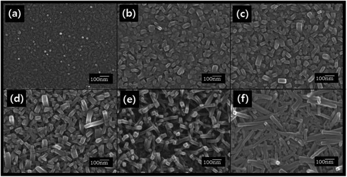 | ||
| Fig. 2 FE-SEM images of the 50 nm thick ZnPc films (a) as-deposited and spray-treated using actone/water mixed solvents at acetone contents (vol%) of (b) 50%, (c) 70%, (d) 86%, (e) 94% and (f) 100%. | ||
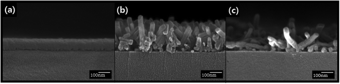 | ||
| Fig. 3 Cross-sectional FE-SEM images of the 50 nm thick ZnPc films (a) as-deposited, (b) acetone/water (94:6 vol%) spray-treated, and (c) acetone-100% spray-treated. | ||
Electronic absorption spectra recorded for the as-deposited ZnPc thin film and the films treated with various solvent sprays are shown in Fig. 4. The absorption of the as-deposited film (Fig. 4a) was indicative of the characteristic α-phase ZnPc. The absorption band, known as the Q-band of phthalocyanine films,21 could be deconvoluted into overlapping four Gaussian curves using the nonlinear least-squares-fitting method. The absorption maxima of three main sub-bands centered at 623 nm, 706 nm, and 747 nm corresponded to the QS, QM, and QL band, respectively.21 The small sub-band at a shorter wavelength of 574 nm was assigned as the vibrationally coupled satellite band.22 The existence of these sub-Q bands was explained by molecular stacking within the phthalocyanine thin films. The QS and QL sub-band corresponded to face-to-face (H-aggregates) and edge-to-edge (J-aggregates) aggregation, respectively.23 The QM band exhibited medium transition aggregates. As shown in Fig. 4(b)–4(e) and the inset in the figure, a gradual change in relative intensities of the sub-bands was observed as the acetone content increased. The intensity of the QS band centered at 623 nm gradually decreased and that of the QL band centered at 747 nm increased. This indicated that a part of the ZnPc molecules in the film was dissolved in acetone and their stacking was alternated toward edge-to-edge aggregation. As shown in Fig. 2 and Fig. 3, the change in the composition of the solvent mixture resulted in a different dimension and orientation of the nanorods. Regarding the orientation, treatment with water-containing acetone (Fig. 3b) was more favorable than treatment with pure acetone (Fig. 3c) since the vertical nanorods are more efficient for the transport of charge carriers in OPV cells.18 However, the remaining water molecules in the film might accelerate the degradation of the cells; thus, post-annealing treatment of the spray-treated films was conducted at temperatures of 100 °C, 200 °C, and 300 °C, for 1 h under high vacuum (base pressure of ∼2 × 10⁻⁸ torr) in order to eliminate the remaining solvent molecules. The AFM images of the non-treated and spray-treated ZnPc thin films at various post-annealing temperatures are presented in Fig. 5(a)–5(c) and Fig. 5(d)–5(f), respectively. All images were taken with the same scan area of 3 μm × 3 μm. The morphology of the as-deposited sample (Fig. 5a) was characterized by tiny spherical crystallites with a root mean square (rms) roughness of 3.77 nm, which is typical of the α-ZnPc polymorph.20 No apparent differences in surface morphology and rms roughness were observed for the samples annealed at 200 °C for 1 h as shown in Fig. 5(b). The longer annealing hardly affected the surface morphology at the annealing temperature up to 200 °C, which is consistent with previous reports for other planar Pc thin films.24,25 In contrast, the film annealed at 300 °C for 1 h contained islands of larger and slightly elongated crystals, indicating that there was a phase transition from α to β polymorph at this annealing temperature (Fig. 5c). AFM images of spray-treated and subsequently post-annealed samples (Fig. 5d–5f) were significantly different from those of non-treated samples. The morphology of the film treated with acetone/water (94:6 vol%) spray (Fig. 5d) was characterized by bundles of nanorods with a rms roughness of 19.7 nm, which was around 5 times larger than that of as-deposited film. Whereas this morphology was retained after post-annealing up to 200 °C (Fig. 5d), the surface of the film annealed at 300 °C was covered with elongated, needle-like crystallites as shown in Fig. 5(f). The variation of electronic absorption for non-treated and spray-treated films after post-annealing is shown in Fig. 6(a)–6(d) and Fig. 6(e)–6(h), respectively. In the case of the non-treated films, little change in peak position and band shape was observed in the spectra for the samples annealed up to 200 °C. In contrast, the spectrum recorded for films annealed at 300 °C showed a peak shift to longer wavelengths, 645 nm and 749 nm, and inversion of the relative intensity (Fig. 6d), which is indicative of a phase transition to β polymorph. In the case of acetone/water (94:6 vol%) spray-treated samples (Fig. 6e), however, annealing at even low temperatures, i.e. 100 °C and 200 °C, led to changes in electronic absorption (Fig. 6f and 6g). As annealing proceeded, the relative intensity of QL sub-band at 747 nm decreased and that of QS sub-band at 623 nm increased. This indicated that some molecules that had stacked edge-to-edge during spray-treatment recovered their initial face-to-face stacking. However, even after 200 °C annealing, the QL sub-band did not disappear completely. We confirmed by X-ray photoelectron spectroscopy (XPS) that the film was dried thoroughly and no oxygen peak was detected. These results indicated that some ZnPc molecules alternated their stacking by solvent spray treatment and the new stacking was stable enough to be retained even after the solvents were dried. For the spray-treated and subsequently 300 °C post-annealed ZnPc thin film, a phase transition to β polymorph was observed (Fig. 6h) as in the case of the non-treated film (Fig. 6d).
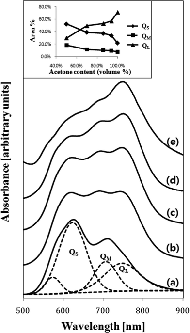 | ||
| Fig. 4 Electronic absorption spectra recorded for the 50 nm thick ZnPc films (a) as-deposited and spray-treated using acetone/water mixed solvents with acetone contents (vol%) of (b) 50%, (c) 70%, (d) 94% and (e) 100%. Example of the deconvolution for the spectrum (a) into four overlapping Gaussian sub-bands is shown. The inset also shows the area% of the three Q sub-bands as a function of acetone content (vol%) in the solvent mixture used. | ||
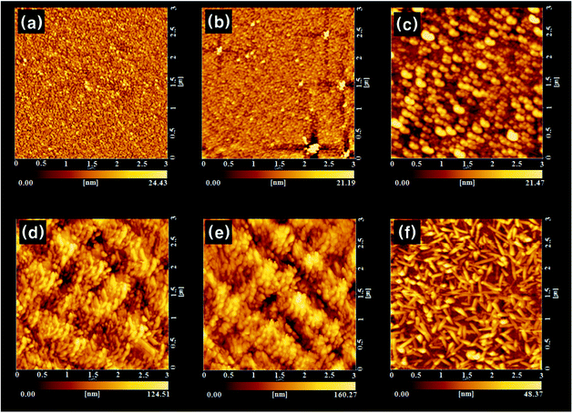 | ||
| Fig. 5
AFM images of the 50 nm thick ZnPc films (a) grown at room temperature and annealed (a) for 1 h at (b) 200 °C and (c) 300 °C, and (d) acetone/water (94:6 vol%) spray-treated and annealed (d) for 1 h at (e) 200 °C and (f) 300 °C. | ||
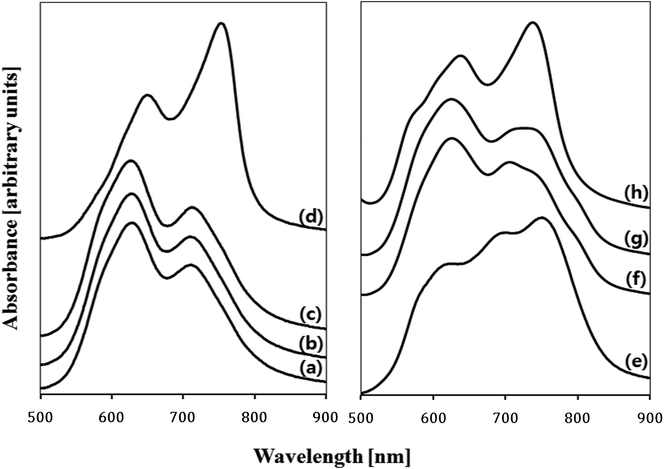 | ||
| Fig. 6
Electronic absorption spectra recorded for the 50 nm thick ZnPc films (a) grown at room temperature and annealed (a) for 1 h at (b) 100 °C, (c) 200 °C and (d) 300 °C, and (e) acetone/water (94:6 vol%) spray-treated and annealed (e) for 1 h at (f) 100 °C, (g) 200 °C and (h) 300 °C. | ||
In conclusion, we developed a novel solvent spray method to fabricate surface nanostructures on molecular thin films. This method is simple and can be applied to most organic films since the composition and amount of solvents are easily controllable. In this work, ZnPc nanorods with various dimensions and orientations were fabricated using the spray of acetone–water mixed solvents with various compositions. In addition to the morphological change, variations in the electronic absorption of the films, i.e. decrease of QS sub-band and increase of QL sub-band, were observed, indicating that a part of ZnPc molecules alternated their stacking from face-to-face to edge-to-edge aggregations. Post-annealing treatment of the spray-treated samples at temperatures up to 200 °C resulted in the recovery of the electronic absorption properties except for a slight increase in the QL sub-band. In contrast, the surface nanostructures formed by the solvent spray treatment were retained even after post-annealing at 200 °C. As a consequence, it is expected that the surface nanostructures of organic thin films can be simply fabricated without a significant change in the light absorption properties.
Acknowledgements
This work was supported by the National Research Foundation (NRF) grant funded by the Ministry of Education, Science and Technology (MEST) of Korea (ERC program, no. R11-2005-048-00000-0).References
- S. R. Forrest, Chem. Rev., 1997, 97, 1793 CrossRef CAS.
- D. J. Gundlach, Y. Y. Lin, T. N. Jackson, S. F. Nelson and D. G. Schlom, IEEE Electron Device Lett., 1997, 18, 87 CrossRef CAS.
- S. Steudel, S. De Vusser, S. De Jonge, D. Janssen, S. Verlaak, J. Genoe and P. Heremans, Appl. Phys. Lett., 2004, 85, 4400 CrossRef CAS.
- D. Cheyns, K. Vasseur, C. Rolin, J. Genoe, J. Poortmans and P. Heremans, Nanotechnology, 2008, 19, 424016 CrossRef.
- D. H. Wang, D. G. Choi, K. J. Lee, J. H. Jeong, S. H. Jeon, O. O. Park and J. H. Park, Org. Electron., 2010, 11, 285 CrossRef CAS.
- D. M. Nanditha, M. Dissanayake, A. A. D. T. Adikaari, R. J. Curry, R. A. Hatton and S. R. P. Silva, Appl. Phys. Lett., 2007, 90, 253502 Search PubMed.
- P. Peumans, S. Uchida and S. R. Forrest, Nature, 2003, 425, 158 CrossRef CAS.
- J. Rostalski and D. Meissner, Sol. Energy Mater. Sol. Cells, 2000, 61, 87 CrossRef CAS.
- F. Yang, M. Shtein and S. R. Forrest, Nat. Mater., 2005, 4, 37 CrossRef CAS.
- F. Yang, M. Shtein and S. R. Forrest, J. Appl. Phys., 2005, 98, 014906 CrossRef.
- G. Günes, H. Neugebauer and N. S. Sariciftci, Chem. Rev., 2007, 107, 1324 CrossRef.
- S. Sun, Z. Fan, Y. Wang and J. Haliburton, J. Mater. Sci., 2005, 40, 1429 CrossRef CAS.
- F. A. Castro, H. Benmansour, C. F. O. Graeff, F. Nesch, E. Tutis and R. Hany, Chem. Mater., 2006, 18, 5504 CrossRef CAS.
- M. C. Orozco, W. C. Tsoi, M. O'Neil, M. P. Aldred, P. Vlachos and S. M. Kelly, Adv. Mater., 2006, 18, 1754 CrossRef CAS.
- X. Liang, T. Chen, Y. S. Jung, Y. Miyamoto, G. Han, S. Cabrini, B. Ma and D. L. Olynick, ACS Nano, 2010, 4, 2627 Search PubMed.
- C. M. Drain, G. Bazzan, T. Milic, M. Vinodu and J. C. Goeltz, Isr. J. Chem., 2005, 45, 255 CrossRef.
- I. Radivojevic, A. Varotto, C. Farley and C. M. Drain, Energy Environ. Sci., 2010, 3, 1897 RSC.
- H. Xi, Z. Wei, Z. Duan, W. Xu and D. Zhu, J. Phys. Chem. C, 2008, 112, 19934 CrossRef CAS.
- C. C. Leznoff, A. B. P. Lever, Phthalocyanines: Properties and Applications, VCH Publishers, New York, 1996 Search PubMed.
- S. Senthilarasu, S. J. Baek, S. D. Chavhan, J. Lee and S. H. Lee, J. Nanosci. Nanotechnol., 2008, 8, 5414 Search PubMed.
- Y. Qiu, P. Chen and M. Liu, Langmuir, 2008, 24, 7200 CrossRef CAS.
- A. W. Snow and N. L. Jarvis, J. Am. Chem. Soc., 1984, 106, 4706 CrossRef CAS.
- M. Kasha, H. R. Rawls and M. Ashraf El-Bayoumi, Pure Appl. Chem., 1965, 11, 371 CrossRef CAS.
- S. Heutz, S. M. Bayliss, R. L. Middleton, G. Rumbles and T. S. Jones, J. Phys. Chem. B, 2000, 104, 7124 Search PubMed.
- S. Yim, S. Heutz and T. S. Jones, J. Appl. Phys., 2002, 91, 3632 Search PubMed.
| This journal is © The Royal Society of Chemistry 2012 |