Multidimensional self-assembly of peanut shaped PbS nanostructures†
Ali Hossain
Khan
a,
Sasanka
Maji
a,
S.
Chakraborty
a,
N. B.
Manik
b and
Somobrata
Acharya
*a
aCentre for Advanced Materials, Indian Association for the Cultivation of Science, Kolkata, 700032, India. E-mail: camsa2@iacs.res.in
bCondensed Matter Physics Research Centre, Department of Physics, Jadavpur University, Kolkata, 700032, India.
First published on 3rd November 2011
Abstract
Peanut shaped PbS nanocrystals are synthesized and their self-assemblies have been studied by means of solvent evaporation. Multi-scale ordered self-assemblies of PbS nanopeanuts have been achieved by solvent evaporation route and interparticle interactions in the solution phase. The self-assembly mechanism produces compact monolayers with long-range ordering over macroscopic areas, which have been utilized for fabricating photovoltaics devices. A current–voltage response upon white light irradiation was measured with increasing photocurrent upon increasing incident light intensity. Repetitive on-off device response to white illumination flux is found to be sharp and repeatable over successive on/off irradiation cycles. Such simple self-assembled route is useful for the fabrication of technologically important ultra thin film materials for sensors and photovoltaic devices.
Introduction
Self-assembly from liquid solutions is a ubiquitous natural phenomenon that can be achieved easily by solvent evaporation. The main idea is to provide a suitable environment in which nanoscale building blocks self-organize spontaneously into ordered structures. In the self-assembly based on evaporation dynamics, where a drop of solvent containing nanoparticles is placed on top of a substrate, the assembly of nanoparticles occurs during drying.1 In most of the cases, self-assembly of the nanomaterials is driven by the forces such as van der Waals forces and hydrogen bonds of organic capping molecules, interaction between crystal facets with preferred reactivity and dipole moments, and capillary forces, etc. Recent examples have demonstrated the self-assembly of ligand passivated nanocrystals during the irreversible evaporation of the solvent.2–10 The relatively weak attractions between nanocrystals, which are screened in solution, become manifest as the solvent evaporates, initiating assembly of slowly evolving structures.2 For example, the surface capping ligands adsorbed on the surface of nanoparticles will direct the assembly process by inter-molecular van der Waals interactions.11–13 Dipolar coupling is another force, which plays role in the self-assembly of nanocrystals into ordered structures.14,15 Wurtzite crystal structures can possess dipole moment owing to the alternate stacking of the anions and cations.16–18 In contrast, rock-salt crystal structure is centrosymmetric and may not possess permanent dipole moments.19 However, rock-salt structure could result in a finite dipole moments depending on the distribution of polar crystal facets.14,19 Recently, Talapin et al. reported on the self-assembled supercrystals of rock-salt PbSe nanocrystals on the basis of dipole moment.20 In addition to the dipolar forces, ordered assemblies of nanomaterials may be achieved with altering a specific shapes.21,22 The morphologies of the resulting assembly can be further engineered by controlling the rate of evaporation and concentration of the solutes among many other factors, which defines the interparticle spacing. Such assemblies are promising means for fabrication of devices from nanomaterials for a variety of novel applications, including sensors,23,24 solar cells,25,26signaling devices,27 and nano-electronic devices.28,29 However, the success of such applications ultimately depend on the processability into large area compact monolayer films.Lead chalcogenide nanocrystals (PbS, PbSe & PbTe) are of current interest because of long range optical tunability from UV-vis to the near IR region.30 The lead chalcogenides have small bulk band gap and exceptionally large exciton Bohr radii, which make them susceptible to carrier quantum confinement effects over a broad range of nanocrystal sizes and shapes.31,32 The discovery of efficient multiple exciton generation by single photons in lead chalcogenide nanocrystals has initiated an intense effort to build lead chalcogenide based photovoltaic devices.33–37 We report on a simple synthesis technique of fabricating unique PbS peanut shaped nanostructures and their multi-scale ordered self-assemblies by solvent evaporation route. Flower like assemblies are obtained at higher concentration which evolves into monodispersed ordered compact film spanning over a large area upon dilution. We show how the morphology of drop-casted PbS peanut films is controlled by evaporation kinetics and interparticle interactions in the liquid phase. The drop-drying process is simple, robust and scalable, and is insensitive to the substrate material, and has a strong preference for forming monolayer films. The self-assembly mechanism produces monolayers with exceptionally compact long-range ordering over macroscopic areas, which have been utilized for fabricating photovoltaics devices. A current–voltage response upon white light irradiation was measured with increasing photocurrent upon increasing incident light intensity. Repetitive on-off device response to white illumination flux is found to be sharp and repeatable over successive on/off irradiation cycles. Such simple self-assembled route is useful for the fabrication of technologically important ultra thin film materials for sensors and photovoltaic devices.
Experimental
Materials
Lead nitrate ([Pb(NO3)2], Aldrich, 99%), thiourea ([SC(NH2)2], Aldrich ≥ 99%), trioctylphosphineoxide (TOPO, Aldrich, 90%) and hexadecylamine (HDA, Aldrich, 90%) were used in as received condition. Anhydrous methanol, chloroform, toluene, dichloromethane and isopropanol were used as solvent for purification, dispersion and device fabrication. Indium tin oxide (ITO) substrate (100 Ω/squares inches) from Aldrich was used as top electrode and Al sheet was used as back electrode.Synthesis of peanut shaped PbS nanoparticles
For the synthesis of peanut shaped nanoparticles, 0.144 g lead nitrate and 0.035 g thiourea were added into 2 g TOPO and allowed to react for 10 min at 110 °C with continuous stirring under nitrogen flow. The temperature was then increased to 160 °C, where the reaction mixture turned into grayish-milky color. At this condition, 0.4 g HDA, which was also kept at 160 °C in a different reaction flask, was injected to the first reaction flask in one shot. The color of the reaction mixture turned to deep reddish black instantaneously, where annealing was carried out for another 60 min. The reaction mixture was then cooled to 70 °C and the reaction was stopped by adding methanol. The peanuts were isolated by washing two times with methanol by centrifugation at 3000 rpm for 3 min. Finally, a mixture of dichloromethane and methanol (1![[thin space (1/6-em)]](https://www.rsc.org/images/entities/char_2009.gif) :8 by volume ratio) was used to remove excess surfactants. A stock solution was then prepared in 10 ml toluene by redispersing the entire precipitated peanuts. The peanut suspension is stable and retains their morphology even after 2 h of sonication.
:8 by volume ratio) was used to remove excess surfactants. A stock solution was then prepared in 10 ml toluene by redispersing the entire precipitated peanuts. The peanut suspension is stable and retains their morphology even after 2 h of sonication.
Device fabrication
Thin film was fabricated on top of a ITO coated glass simply by drop casting using a PbS peanuts solution of 3.33 millimolar (mM) concentration. Sandwiched pattern devices were fabricated using Al sheets as counter electrode on the top of the PbS peanuts film.Sample characterization
Powder X-ray diffraction (XRD), scanning electron microscopy (SEM), transmission electron microscopy (TEM), high-resolution TEM (HRTEM), and selected area electron diffraction (SAED) were adopted to characterize the size, shape and structure of synthesized PbS nanoparticles. XRD analysis of the PbS peanuts was carried out by Rigaku XRD instrument (λ = 1.5405 Å). TEM, HRTEM and SAED were performed using a JEOL 2010 transmission electron microscope after putting a drop of particle suspension in lacey carbon coated copper grid followed by drying of the sample. SEM analysis was performed on a JEOL field emission scanning electron microscope (JSM-6700F) operating at an accelerating voltage of 5 kV after drop casting PbS Peanuts suspension on glass and drying overnight in air followed by platinum coating. For photovoltaic measurements, the current flowing through the device was estimated by measuring a voltage drop (measured using Agilent Model No. 34970A) across 56 KΩ sensing resistance. The light source for photovoltaic measurement was a 200 W tungsten lamp and the light intensity was measured by a calibrated lux meter (Kyoritsu Electrical Instruments Work Ltd. Tokyo, model 5200).Results and discussion
We have prepared PbS nanostructures by using mixture of TOPO and HDA as capping agents. Presumably both the ligands passivate the nanocrystal surfaces while the delicate balance among two different types of ligands and their injection temperature determines the shape, dispersity and interparticle separation (see ESI†, Fig. S1). We have purified the as-prepared PbS nanostructures and redispersed them in toluene to obtain a clear stable reddish colloidal suspension. The estimated concentration (CPbS) of this stock solution is approximately 40 mM, which is calculated by accounting the moles of the reagents used. One drop (typically ∼5 μL) of PbS suspension was cast onto a substrate (cover glass) and dried in air. The dried droplet was first investigated using SEM. Fig. 1 shows the SEM images at different magnification of the drop casted as-prepared PbS nanostructures stabilized by TOPO and HDA. The lower resolution image (Fig. 1a) reveals flower like structures with flecks of nearly 5 μm width as the petals of the flower. Some petals at the centre of the flower are found to be standing vertically with respect to the substrate while the rests are slanted in an acute angle with respect to the substrate. Zooming in the petals (Fig. 1b) reveals that the petals are constructed with a large number of closely packed particles. Further higher resolution SEM image (Fig. 1c) reveals that the petals are actually formed by uniform peanut shaped nanoparticles, where the peanuts are stacked in closed packed manner. The typical width of the peanut shaped particles are around 100 nm.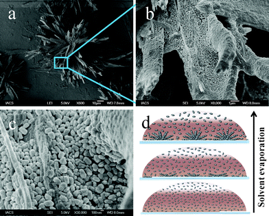 | ||
| Fig. 1 SEM images of concentrated peanut shaped PbS nanoparticles with (a) flower like structures, (b) and (c) are the higher resolution SEM image of a part of the PbS flower showing the assembly of peanuts. (d) Schematic showing droplet-evaporation-induced formation of flower likes nanostructures by the peanut shaped PbS nanoparticles. | ||
The flowers and the petals are likely to form as a result of the strong interparticle interactions forming standing morphologies. In cases, the petals are observed growing from the centre of the flower with repetitive layered stacking. Nanoparticles may exhibit a range of ordered two or three dimensional assembled structures easily upon solvent evaporation and the process is highly sensitive to the concentration of the particles.38 During evaporation of the droplet of PbS peanut suspension, an in-plane compression developed due to the decrease in the surface area, concurrently the concentration of peanuts within droplet is gradually increases (Fig. 1d). When the concentration of peanuts within the droplet increases up to the super saturation point as a result of solvent evaporation, PbS peanuts start sedimentation on top of the substrate. Since the concentration of the peanut particles changes with drying time, the sedimentation process is continuous leading to the close packed layered stacking of the peanuts. Such continuous process of stacking might lead to the vertically standing flecks as a result of increasing concentration at the end of the evaporation process. Because of strong interparticle interaction between the peanuts a continuous fleck structure occurs.
The in-plane packing of the peanuts is found to vary depending on the concentration of peanuts and with the evaporation rate of the solvent used (see ESI†, Fig. S2).38 In order to investigate the effect of concentration on the self assembly of PbS peanuts, we carried out concentration dependent evaporation rate study of the as-synthesized peanuts by drop casting on top of solid substrate.
Simultaneously, we attempted to identify an optimum condition for obtaining a large area of ordered monolayer of the peanuts during the evaporation process. We observed that the flowers break into the three-dimensional (3D) stacked assembled petals (Fig. 2a) with the dilution (CPbS = 10 mM) of the mother suspension (CPbS = 40 mM). Upon further dilution (CPbS = 5 mM), the petals appear flat while the peanuts still remain in tightly packed configuration within the petals (Fig. 2b). Continuing the dilution process (CPbS = 3.33 mM) further led to a large area self assembled 2D compact monolayer of closely packed peanuts (Fig. 2c). Upon further dilution (CPbS = 2.5 mM), better dispersion is obtained within a closed packed monolayer of individual peanuts (Fig. 2d), indicating that the concentrations of the PbS peanuts significantly affect the self-assembly of these structures.
 | ||
| Fig. 2 SEM images of self-assembled structures of PbS peanuts for different concentrations: (a) Flacks from 10 mM solution. (b) Plates from 5 mM solution. (c) Closed packed film from 3.33 mM solution. (d) Monolayer film from 2.5 mM solution. | ||
Detailed structural and morphological investigations were carried out using XRD and HRTEM analysis. The XRD pattern of the as-prepared PbS peanuts shows a high degree of crystallinity (Fig. 3). Most of the peaks match well with Bragg reflection conditions of the standard face-centred cubic (fcc) structure of bulk PbS (JCPDS #05-0592). The XRD reveals sharp intense (200) diffraction peaks and a relatively broader (111) diffraction peaks. It is also worth noting that the ratio between the intensities of the (200) and (111) diffraction peaks is 1.202 which is somewhat higher than the reported value (1.049) indicating that the peanuts may be abundant in {100} facets, and grow along the <100> directions. Moreover, some additional weak intense peaks are also observed in the XRD patterns, which are not matching with the cubic PbS phase, are the contributions from the unremoved surfactants (see ESI†, Fig. S3).
 | ||
| Fig. 3 The XRD of the drop casted films of the purified peanut shaped PbS nanoparticles, which matches well to the standard cubic rock-salt structure with strongest (200) reflection. The expected positions and intensities of the standard peaks rock-salt cubic PbS (JCPDS #05-0592) are indicated by blue vertical lines. | ||
The morphology and crystallinity of the PbS peanuts was further investigated using TEM. The typical TEM image of the PbS nanostructures (Fig. 4a) clearly shows that peanuts are of nearly identical in size with an average diameter of 100 nm. HRTEM (Fig. 4b) confirms the crystallinity showing well-resolved lattice planes with an inter-planar distance of 0.29 nm corresponding to (200) planes of PbS bulk rock salt structure. Notably, the HRTEM measurement points out to a local structure, while the XRD pattern is representing the global nature of the sample. However, both these techniques together may represent the crystal structure of the entire sample and both indicate an orientation in which the <100> crystallographic axis is parallel to the growth axis of the peanuts. The SAED patterns (Fig. 4c) shows the predominant 200, 220 and 311 diffraction spots, corresponding to the inter-planer distances of 0.29 nm, 0.24 nm and 0.20 nm of PbS bulk rock salt structure (JCPDS powder diffraction file #05-0592) respectively. The strongest intensity of the 200 reflection is supportive to the previous XRD and HRTEM observations.
 | ||
| Fig. 4 (a) TEM image of peanut shaped PbS nanoparticles. The zoom of the selected portion of the main figure (Fig. 4a) is shown in the inset and it's demonstrating the presence of small cubic shaped PbS nanoparticles along with the peanuts. (b) HRTEM image of PbS peanuts with well resolved lattice planes. The inter-planner distance of 0.29 nm corresponds to the (200) sets of d-spacings. (c) SAED pattern from the peanuts visible in Fig. 4a. (d) HRTEM image of small cubic PbS nanoparticles present at the edge of the peanuts with well resolved lattice fringes corresponding to inter-planar distance of 0.29 nm, consistent with the (200) planes of PbS bulk rock salt structure. | ||
The TEM image (Fig. 4a) reveals the existence of few small sized particles near the periphery of the peanuts, which were not observed in SEM. Higher resolution TEM image (inset of Fig. 4a) shows that these small particles are PbS cubes of 10 nm size. The HRTEM image of the PbS cubes (Fig. 4d) shows well-resolved lattice spacings corresponding to (200) PbS planes, the same as peanuts. The coexistence of cubes along with the peanuts in an identical crystal structure might point out to the mechanism of growth direction of the peanuts.
To investigate the formation mechanism of the peanuts, we carried out control reactions by tuning the nature of ligands. First, we have carried out the reaction for 10 min at 110 °C by injecting lead nitrate and thiourea into TOPO only. The temperature was then increased to 130 °C, where the reaction was stopped immediately when the reaction mixture turned to milky-gray color. Flat bundle like aggregated whiskers are evidenced in this reaction condition, while surprisingly maintaining uniformity in the width around 100 nm (see ESI†, Fig. S4). These aggregated whiskers turned into bundles of tightly bounded rods upon increasing the reaction temperature to 160 °C and annealing for 60 min (see ESI†, Fig. S5). These control reactions supports that HDA is essential for PbS peanut shape formation. In the absence of HDA, aggregated whiskers turned into bundle of tightly bounded rods. We have injected HDA in the reaction mixture after formation of whiskers aggregates in TOPO in a separate reaction condition to obtain the peanuts. The use of HDA prevents further growth of whiskers aggregates resulting in peanuts of similar dimension.
The structure of initial PbS seed that form PbS peanuts may consists of a truncated cuboctahedron with six {100} facets, eight {111}, and twelve {110} facets as demonstrated previously for crystalline equivalent lead chalcogenide systems.14,39 During crystal growth, the seed will minimize the most energetically unfavourable facets and removal of the {111} and {110} facets were earlier observed during the nanoparticle growth.14,39 We anticipate a similar growth mechanism leading to the peanuts using mixture of HDA and TOPO and bundles of nanorod aggregates using TOPO only (Fig. 5). The chemical nature of stabilizing capping agents is significantly affecting the facet energies and the growth of PbS nanocrystals. Presumably, TOPO adsorb on the {100} facets of PbS nucleating seeds resulting in truncated cuboctahedron particles with mainly {100} planes. With increasing the reaction temperature, {100} facets becomes highly reactive and are preferentially consumed yielding whiskers like aggregate and bundle of rod aggregates at elevated temperature (Fig. 5, Path 1). In fact, a thermal gradient may lead to a growth toward the high-temperature side as reported by Wagner and the growth rate can have a striking effect on the resultant morphology.40 When hot HDA is injected into the reaction mixture, HDA prevents the oriented attachment process owing to the presence of long aliphatic chain leading to the peanuts shaped PbS (Fig. 5, Path 2). The uncoalesced truncated cuboctahedron which were weakly attached to the periphery of the peanuts as observed in TEM turned into cubes after HDA injection by the elimination of the {111} facets.
 | ||
| Fig. 5 Schematic diagram of PbS whiskers like aggregate (path 1a), bundle of rod aggregates (path 1b) and peanut (path 2) formation from small PbS truncated cuboctahedron which was the nucleating seed. | ||
Notably, the controlled assembly of peanuts is obtained by means of drop casting and simultaneously drying routes without using an external driving force such as electric field or pressure induced assemblies to bring the peanuts into closer proximity.41,42 This predicts that controlling the interaction between the peanuts in the liquid phase is the key to the realization of highly ordered aggregates. Since the peanuts are capped with both TOPO and HDA, an organic shell is formed by the ligands around the PbS core. The van der Waals interaction among the shells and the inherent dipole moment provides the attractive force to induce the self-assembly, where as the steric repulsion due to the ligand interdigitation provides the balancing force to create a stable structure. In fact a finite dipole moment may exist in PbS nanocrystal owing to the asymmetric structure, the magnitude of which depends on the size and volume of the nanocrystal.43 The mixed {100} and {110} facets are formed by both Pb and S atoms, while the {111} facets consist of either S or Pb atoms. Due to the difference in electro-negativities between Pb and S, {111} facets are polar and their arrangement will determine the net electric charge distribution and dipole moment within the PbS nanocrystal.
The nature of assembly and packing of the peanuts within the flowers and petals are highly dependent on concentration and solvent evaporation rate. Since toluene is a high boiling solvent, the peanuts find enough time to orient them in the suspension phase at their favourable orientation in comparison to a low boiling solvent such as dichloromethane (see ESI†, Fig. S2). When the solvent molecules evaporate from the top surface of a concentrated drop, the dispersed peanuts at the air-toluene interface can diffuse into the drop interior creating a steep concentration gradient resulting in a supersaturated environment within the drop with drying time.44 An in-plane compression developed due to the decrease in the surface area along with the change in the contact angle of the droplet with the substrate. Concurrently, the concentration of peanuts is gradually increased as a result of solvent evaporation. When the concentration of peanuts within the droplet increases up to the super saturation point, PbS peanuts start sedimentation on top of the substrate. However, in a closed packed configuration, the minimum separation distance between two adjacent peanuts is defined by the layer thickness of the organic shell formed by TOPO and HDA. Hence a bi-layer of the surfactants is always expected between adjacent peanuts even in supersaturated environment. In supersaturated environment, the van der Waals interaction between the ligand shells and the inter PbS dipolar interaction are supposed to be strong enough owing to the shorter interparticle distances. Since the concentration of the peanut particles increases with the evaporation process, the continuous sedimentation process leads to the standing flacks and flower-like structures of closely packed peanuts. Upon dilution, the interparticle separation distances increases and the van der Waals and dipolar interaction reduces resulting in the flowers to break into the closely packed assembly petals. Upon further dilution, at a critical concentration, a large area 2D self assembled compact monolayer of peanuts can be achieved. However, as these monolayers extend over macroscopic dimensions, the upper limit for the area to be covered depends on the droplet size and the concentration of peanuts.
We fabricated photovoltaic devices making use of uniformity, dimensionality and packing of these self-assembled structures. The self-assembled PbS films are important in exciton migration owing to the close packing of the peanuts.45 We have fabricated thin film photovoltaic devises by drop casting PbS peanut suspension using 3.33 mM concentration on indium tin oxide (ITO) substrates (Aldrich, 100 Ω/squares inches). A sandwiched pattern device has been fabricated using Al sheet as counter electrode. We deliberately avoided the use of any additional layer which may enhance the photovoltaic property or other post-preparative process such as ligand exchange for photovoltaic measurement purposes.35–37 We have tested photovoltaic response of the devices in ambient condition. The current–voltage characteristics in dark and under 64.6 mW cm−2 irradiation when exposed to an active area of 9 mm2 are shown in Fig. 6a.
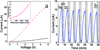 | ||
| Fig. 6 (a) Current–voltage characteristics of pure peanut shaped PbS nanocrystals films with (red dotted curve) and without (black curve) illumination with respect to external applied voltage. The inset shows the current vs. light intensity plot (b) Photo switching performance of peanut shaped PbS nanoparticles film on illumination. The light source for photovoltaic measurement was a 200 W tungsten lamp. | ||
In the case of the dark measurement, the current increases up to 4.5 μA with the increase in voltage up to 5V. Upon illumination of light, the current increases sharply resulting in orders of enhanced current. With the increase in light intensity, the photocurrent increases exponentially as expected (inset of Fig. 6a). The photoswitching responses of these devices show uniform on-off cycles in presence and absence of light illumination respectively (Fig. 6b). The repetitive on-off device response to white illumination flux was found to be sharp and repetitive over successive on/off cycles (Fig. 6b). Photocurrent increased sharply upon light exposure and decays linearly in the subsequent absence of light source while retaining reproducibility in successive on-off cycles. The long term photo switching property suggests a higher stability of the devises. The device performance retains even after several days after keeping in open air defining the stability of the devises.
Conclusions
In summary, we have demonstrated a simple method for the synthesis of monodispersed peanut shaped PbS nanocrystals. Control over the reactions has been achieved by controlling the amount of precursors, surfactant and by controlling the reaction temperature. We have investigated the effect of surfactant on PbS peanut shape formation. We have also demonstrated a simple method for assembling the PbS peanuts into a compact film, which can be achieved simply by the evaporation of the dispersing solvent. Preliminary photovoltaic measurements by making compact self assembled monolayer films, which helps in exciton migration owing to the close packing suggests potential for photovoltaic applications. Our method is quite flexible since the ordered assembly can be precisely controlled in the sub-micron range by varying applied surface pressure.Acknowledgements
Financial support under Grant #SR/S5/NM-47/2005 and Grant# SR/NM/NS-49/2009 from DST, India are gratefully acknowledged. The authors are thankful to Professor D. D. Sarma for scientific advises. AHK acknowledge CSIR, India for funding.References
- E. Rabani, D. R. Reichman, P. L. Geissler and L. E. Brus, Nature, 2003, 426, 271–274 CrossRef CAS.
- J. Tang, G. Ge and L. E. Brus, J. Phys. Chem. B, 2002, 106, 5653–5658 CrossRef CAS.
- V. F. Puntes, K. M. Krishnan and A. P. Alivisatos, Science, 2001, 291, 2115–2117 CrossRef CAS.
- G. M. Whitesides and B. Grzybowski, Science, 2002, 295, 2418–2421 CrossRef CAS.
- C. B. Murray, C. R. Kagan and M. G. Bawendi, Science, 1995, 270, 1335–1338 CrossRef CAS.
- R. G. Freeman, K. C. Grabar, K. J. Allison, R. M. Bright, J. A. Davis, A. P. Guthrie, M. B. Hommer, M. A. Jackson, P. C. Smith, D. G. Walter and M. J. Natan, Science, 1995, 267, 1629–1632 CrossRef CAS.
- R. P. Andres, J. D. Bielefeld, J. I. Henderson, D. B. Janes, V. R. Kolagunta, C. P. Kubiak, W. J. Mahoney and R. G. Osifchin, Science, 1996, 273, 1690–1693 CrossRef CAS.
- R. P. Sear, S. W. Chung, G. Markovich, W. M. Gelbart and J. R. Heath, Phys. Rev. E, 1999, 59, R6255–R6258 Search PubMed.
- T. Fried, G. Shemer and G. Markovich, Adv. Mater., 2001, 13, 1158–1161 CrossRef CAS.
- F. X. Redl, K.-S. Cho, C. B. Murray and S. O'Brien, Nature, 2003, 423, 968–971 CrossRef CAS.
- Z. L. Wang, S. A. Harfenist, I. Vezmar, R. L. Whetten, J. Bentley, N. D. Evans and K. B. Alexander, Adv. Mater., 1998, 10, 808–812 CrossRef CAS.
- C. J. Loweth, W. B. Caldwell, X. G. Peng, A. P. Alivisatos and P. G. Schultz, Angew. Chem., Int. Ed., 1999, 38, 1808–1812 CrossRef CAS.
- W. Feng, L.-D. Sun and C.-H. Yan, Langmuir, 2011, 27, 3343–3347 CrossRef CAS.
- K. S. Cho, D. V. Talapin, W. Gaschler and C. B. Murray, J. Am. Chem. Soc., 2005, 127, 7140–7147 CrossRef CAS.
- Z. Tang, Z. Zhang, Y. Wang, S. Glotzer and N. Kotov, Science, 2006, 314, 274–278 CrossRef CAS.
- S. A. Blanton, R. L. Leheny, M. A. Hines and P. Guyot-Sionnest, Phys. Rev. Lett., 1997, 79, 865–868 CrossRef CAS.
- L.-S. Li and A. Alivisatos, Phys. Rev. Lett., 2003, 90, 097402 CrossRef.
- S. Acharya, A. B. Panda, S. Efrima and Y. Golan, Adv. Mater., 2007, 19, 1105–1108 CrossRef CAS.
- M. Shim and P. Guyot-Sionnest, J. Chem. Phys., 1999, 111, 6955–6964 CrossRef CAS.
- D. V. Talapin, E. V. Shevchenko, C. B. Murray, A. V. Titov and P. Kral, Nano Lett., 2007, 7, 1213–1219 CrossRef CAS.
- Q. Song, Y. Ding, Z. L. Wang and Z. J. Zhang, J. Phys. Chem. B, 2006, 110, 25547–25550 CrossRef CAS.
- R. Zheng, H. Gu, B. Xu, K. K. Fung, X. Zhang and S. P. Ringer, Adv. Mater., 2006, 18, 2418–2421 CrossRef CAS.
- C. J. Brinker, Y. Lu, A. Sellinger and H. Fan, Adv. Mater., 1999, 11, 579–585 CrossRef CAS.
- S. I. Stupp, V. LeBonheur, K. Walker, L. S. Li, K. E. Huggins, M. Keser and A. Amstutz, Science, 1997, 276, 384–389 CrossRef.
- J. Nelson, Science, 2001, 293, 1059–1060 CrossRef CAS.
- L. Schmit-Mende, A. Fechtenkotter, K. Mullen, E. Moons, R. H. Friend and J. D. MacKenzie, Science, 2001, 293, 1119–1122 CrossRef CAS.
- K. Rajangam, H. A. Behanna, M. J. Hui, X. Han, J. F. Hulvat, J. W. Lomasney and S. I. Stupp, Nano Lett., 2006, 6, 2086–2090 CrossRef CAS.
- D. V. Talapin and C. B. Murray, Science, 2005, 310, 86–89 CrossRef CAS.
- G. Konstantatos, I. Howard, A. Fischer, S. Hoogland, J. Clifford, E. Klem, L. Levina and E. H. Sargent, Nature, 2006, 442, 180–183 CrossRef CAS.
- J. J. Peterson and T. D. Krauss, Nano Lett., 2006, 6, 510–514 CrossRef CAS.
- I. Kang and F. W. Wise, J. Opt. Soc. Am. B, 1997, 14, 1632–1646 Search PubMed.
- G. E. Tudury, M. V. Marquezini, L. G. Ferreira, L. C. Barbosa and C. L. Cesar, Phys. Rev. B, 2000, 62, 7353–7364.
- R. J. Ellingson, M. C. Beard, J. C. Johnson, P. R. Yu, O. I. Micic, A. J. Nozik, A. Shabaev and A. L. Efros, Nano Lett., 2005, 5, 865–871 CrossRef CAS.
- R. D. Schaller and V. I. Klimov, Phys. Rev. Lett., 2004, 92, 186601 CrossRef CAS.
- S. A. Mcdonald, G. Konstantatos, S. Zhang, P. W. Cyr, E. J. D. Klem, L. Levina and E. H. Sargent, Nat. Mater., 2005, 4, 138–142 CrossRef CAS.
- V. Sukhovatkin, S. Hinds, L. Brzozowski and E. H. Sargent, Science, 2009, 324, 1542–1544 CrossRef CAS.
- E. H. Sargent, Nat. Photonics, 2009, 3, 325–331 CrossRef CAS.
- A. Boker, J. He, T. Emrick and T. P. Russell, Soft Matter, 2007, 3, 1231–1248 RSC.
- C. Schliehe, B. H. Juarez, M. Pelletier, S. Jander, D. Greshnykh, M. Nagel, A. Meyer, S. Foerster, A. Kornowski, C. Klinke and H. Weller, Science, 2010, 329, 550–553 CrossRef CAS.
- R. S. Wagner, In Whisker Technology; Levitt, A.P., Ed.; Wiley Interscience: New York, 1970; p-47 Search PubMed.
- M. Grzelczak, J. Vermant, E. M. Furst and L. M. Liz-Marzan, ACS Nano, 2010, 4, 3591–3605 CrossRef CAS.
- S. Acharya and S. Efrima, J. Am. Chem. Soc., 2005, 127, 3486–3490 CrossRef CAS.
- S. Kundu, J. P. Hill, G. J. Richards, K. Ariga, A. H. Khan, U. Thupakula and S. Acharya, ACS Appl. Mater. Interfaces, 2010, 2, 2759–2766 CrossRef CAS.
- T. P. Bigioni, X.-M. Lin, T. T. Nguyen, E. I. Corwin, T. A. Witten and H. M. Jaeger, Nat. Mater., 2006, 5, 265–270 CrossRef CAS.
- J. J. H. Pijpers, R. Ulbricht, K. J. Tielrooij, A. Osherov, Y. Golan, C. Delerue, G. Allan and M. Bonn, Nat. Phys., 2009, 5, 811–814 CrossRef CAS.
Footnote |
| † Electronic Supplementary Information (ESI) available: Additional discussions, SEM and TEM images. See DOI: 10.1039/c1ra00321f/ |
| This journal is © The Royal Society of Chemistry 2012 |