Enhanced material purity and resolution via synchronized laser assisted electron beam induced deposition of platinum†
Nicholas A.
Roberts
ab,
Jason D.
Fowlkes
c,
Gregory A.
Magel
a and
Philip D.
Rack
*bc
aOmniprobe Inc., an Oxford Instruments Company, Dallas, TX, USA. Tel: +1 214 572 6800
bDepartment of Materials Science and Engineering, University of Tennessee, Knoxville, TN, USA. E-mail: prack@utk.edu; Fax: +1 865 974 4115; Tel: +1 865 974 5344
cCenter for Nanophase Materials Sciences, Oak Ridge National Laboratory, Oak Ridge, TN, USA. Fax: +1 865 574 1753; Tel: +1 865 223 2902
First published on 13th November 2012
Abstract
We introduce a laser assisted electron beam induced deposition (LAEBID) process which is a nanoscale direct write synthesis method that integrates an electron beam induced deposition process with a synchronized pulsed laser step to induce thermal desorption of reaction by-products. Localized, spatially overlapping electron and photon pulses enable the thermal desorption of the reaction by-product while mitigating issues associated with bulk substrate heating, which can shorten the precursor residence time and distort pattern fidelity due to thermal drift. Current results demonstrate purification of platinum deposits (reduced carbon content by ∼50%) with the addition of synchronized laser pulses as well as a significant reduction in deposit resistivity. Measured resistivities from platinum LAEBID structures (4 × 10³ μΩ cm) are nearly 4 orders of magnitude lower than standard EBID platinum structures (2.2 × 10⁷ μΩ cm) from the same precursor and are lower than the lowest reported EBID platinum resistivity with post-deposition annealing (1.4 × 10⁴ μΩ cm). Finally the LAEBID process demonstrates improved deposit resolution by ∼25% compared to EBID structures under the conditions investigated in this work.
Introduction
Electron beam induced deposition (EBID) is a nanoscale direct write synthesis method in which a focused electron beam locally induces the dissociation of a substrate-adsorbed precursor molecule. A portion of the dissociated molecule condenses at the electron–substrate–precursor interface. EBID is frequently used for mask repair1–3 and nanolithography,4,5 but has also been used in processing for nanoscale welding,6–9 scanning probe microscopy (SPM) probes,10–12 growth of magnetic nanowires for magnetic storage, sensing and logic applications,13,14 fabricating nanoscale strain sensors,15 fabricating electron sources,16 nano optics,17 nanoscale gripping devices (nanotweezers),18 cages for nanoparticle separator,19 diodes20 and as seeds for nanofiber growth21 and atomic layer deposition.22Typical EBID conditions are at room temperature, thus the non-volatile by-products (typically carbon containing ligands from organometallic precursor) remain on the surface and with subsequent deposition layers become embedded in the deposited material, which has been a severe limitation for many functional nanoscale device applications. As an example, EBID is used to deposit conducting electrodes to contact various nanoscale elements, however, the carbonaceous deposits have resistivities which are typically 2–7 orders of magnitude greater relative to pure metals.23–25 A couple of exceptions to the typically higher resistivity are demonstrated in work by Fernandez-Pacheco et al. which showed near bulk cobalt resistivity without post-processing26 and Klein et al. which showed single-crystal tungsten nanowires from WF6 without additional processing.27 Many purification methods have been used to reduce the carbon concentration including annealing of the structures after deposition,28–30 deposition onto heated substrates,31,32 variation in deposition parameters (beam current, precursor flux, scanning method),30,33,34 introducing a reactive gas into the chamber during deposition,35 the use of carbon-free precursors33,36–38 and various other in situ and ex situ processes.15,30,39,40 For additional information on purification methods see the review article by Botman et al.41
While post-synthesis thermal treatments have demonstrated the ability to improve the deposit purity, the annealed deposits undergo morphological changes in their shape and size. Previously substrate heating has been introduced for EBID and gallium focused ion beam induced deposition with the use of a well-controlled heated stage28 as well as focused continuous wave (cw) laser irradiation.42 Higher deposit purities have been reported for some precursor chemistries, but are often accompanied by reduced growth rates due to reduced precursor residence times at elevated temperatures. Furthermore, bulk substrate heating can lead to thermal drift, and in some cases devices and/or structures on the substrate cannot undergo elevated temperature processing.
The pulsed laser assisted electron beam induced deposition (LAEBID) approach described in this paper demonstrates thermally stimulated desorption of the EBID reaction by-products using a laser pulsing strategy to facilitate desorption at the monolayer scale. Moreover, precursor residence times during the electron dwell period are unaffected because (1) the laser pulse follows immediately after the electron dwell and (2) the laser pulse is brief with respect to the total precursor refresh period. Additionally, as will be demonstrated, thermal drift during deposition is mitigated via the synchronized electron and laser beam exposure as shown in Fig. 1 where the brief laser exposure results in high heating and cooling rates to reduce prolonged thermal transients (i.e. no thermal drift or expansion). Synchronized electron and photon pulsing, along with a steady-state gas flow, result in the effective precursor and by-product surface coverage and substrate surface temperature profiles shown qualitatively in Fig. 1(b). Briefly, the cycle begins with a pulsed and scanned electron beam induced deposition cycle in which ∼1 to several monolayers of EBID deposit is formed. Subsequent to EBID, a pulsed laser irradiates the EBID region. Photons are absorbed and locally heat the deposited material sufficiently to desorb contaminant by-products. The photon energy remains below a pyrolytic laser chemical vapor deposition threshold (and using a wavelength below a photolytic threshold). Finally, there is a refresh time in which the temperature decays back to room temperature and precursor replenishes the EBID region for subsequent growth.
 | ||
| Fig. 1 (a) Schematic of LAEBID within the SEM system. (b) Timing diagram of the electron and laser beam exposure as well as the precursor and by-product concentration on the surface and the surface temperature (note that although the precursor coverage varies the gas flux remains constant throughout the process). (c) Chamber view of the electron column, gas injection nozzle and laser optics. | ||
Results and discussion
Methods
The experimental setup for LAEBID is also shown in Fig. 1(c) in which a laser delivery probe (from Omniprobe, Inc.) attached to the chamber of an FEI, Inc. Nova 600 NanoLab DualBeam™ allows a fiber-pigtailed 915 nm 25 W multi-chip diode laser module (Oclaro, BMU25B-915-01) to deliver high-powered laser pulses (∼100 μm diameter) to the substrate surface. The laser is controlled by a 10 A quasi-cw pulsed diode laser driver (IXYS Colorado/Directed Energy, PCX-7410). The laser diode driver is operated in external mode and is triggered by the pattern generator system (Raith, ELPHY Quantum). For more information about the laser delivery system and applications see ref. 43.The Raith patterning software is programmed to write a specified area using a serpentine scanning routine. After each loop through the pattern the electron beam is blanked, triggering the laser pulse. The main difference between LAEBID and other EBID purification methods is the pseudo-localized and temporally confined laser heating. The laser delivery probe allows the area of interest to be heated (resulting in desorption of unwanted by-products) without the need to heat the entire substrate; heating of the entire substrate introduces additional problems as discussed above. Pulsed laser operation is ideal because it allows interaction with the near-surface region (compared to cw, which results in greater thermal penetration in the steady state). In addition to the benefits of the short and localized pulsing on thermal effects, there are also benefits in desorption of by-products due to the rapid heating. For instance, Burgess et al.44 demonstrated that the laser pulse shape as well as the power influences the time evolution of the surface temperature and can have a significant impact on the peak surface temperature. Higher surface temperatures result in reduced residence time (thermal desorption time). Based on their work, complete thermal desorption of the by-product can be achieved if the laser irradiance and pulse width combined cause a surface temperature rise large enough to exceed the by-product desorption threshold. Thermal modeling of the laser–substrate interaction for different pulse widths and irradiances can be found in the ESI.†
Purification of EBID using the LAEBID method is demonstrated on both square pads for energy dispersive X-ray spectroscopy (EDS) measurements and rectangular areas deposited across four point probe structures for resistivity measurements. Prior to any deposits a 15 minute plasma chamber clean (XEI Scientific, Inc., Evactron Decontaminator) was performed and the chamber was allowed to pump several hours (usually overnight) to achieve a base pressure of 5 × 10⁻⁷ Torr. During deposition the chamber pressure remained steady at 6 × 10⁻⁶ Torr after the valve for the precursor gas was opened. The 500 μm outer diameter (OD) gas nozzle was located 120 μm from the substrate surface and 50 μm from the center of the electron beam (∼475 μm from the focal point at ∼40 degree angle). Square pads of approximately 500 nm × 500 nm were deposited onto a 50 nm Ti/100 nm thermal oxide/Si substrate. A beam energy of 5 keV and a beam current of 400 pA was used to deposit the square pads. A dwell time of 50 μs per pixel is used for a total of 1000 pixels (15.8 nm pixel spacing). Each area was repeated a minimum of 1000 times to ensure a thick deposit (>200 nm) for EDS measurements. At the end of the electron write period (∼50 ms) the electron beam is blanked and the laser pulse is triggered (variable pulse width and power). The Ti film on the thermal oxide substrate aids in absorption of the photon energy while the oxide layer provides thermal isolation from the bulk Si substrate. For different precursors the substrate and laser conditions need to be chosen with particular interest in the reflectivity and absorption at the wavelength of the photon beam as well as the thermal conductivity, heat capacity and emissivity in order to effectively heat the substrate without resulting in thermally stimulated decomposition of the precursor or excessive thermal drift. The laser pulse is then followed by a precursor gas refresh period (∼100 ms) to allow the surface to cool and fresh precursor to adsorb onto the substrate surface for the next electron exposure period. Thermal simulations show that the substrate cools to ambient temperature prior to the start of the next electron beam dwell cycle (see ESI†).
Rectangular area deposits were also performed for four point probe resistivity measurements. These deposits were patterned across ∼100 nm thick gold electrodes on a 500 nm thermal oxide on a silicon substrate. The deposited areas were 20 μm long and 300 nm wide (see ESI†). The beam conditions were the same as for the square pads (5 keV and 400 pA) however a larger total number of 5000 loops was used for electron beam exposures. The larger write area made the write period ∼100 ms while the refresh period remained at 100 ms. The thickness of the areas was dependent on the laser conditions used during the deposition process (due to densification and the removal of carbon). Under high laser heating loads (high irradiance and long laser pulse widths) precursor coverage can be depleted also resulting in a reduced deposition thickness. The laser pulse width and power were varied in both the square pads and lines for subsequent EDS and resistivity measurements. In addition to these laser parameter studies, the electron beam dwell time and current were also varied in order to investigate the limitations of the laser assist method for purification as the deposit thickness increases per loop.
To characterize the deposits both EDS and resistivity measurements were performed. EDS of the square pads was performed within the same Nova 600 NanoLab with an EDAX Genesis X-ray Microanalysis System using 5 keV and 1.6 nA at a working distance of 5.1 mm. The chamber was not vented between deposition and EDS measurements. The EDS measurements were taken in spot mode with a 30 second acquisition time. The 30 second acquisition time was sufficient to distinguish noticeable platinum and carbon peaks (∼120k counts). For each EBID and LAEBID condition multiple pads were deposited and measured to account for any statistical variation in the deposit purity. Calculation of the atomic concentration of platinum with respect to carbon was accomplished using a previously measured and verified reference platinum EBID structure from Plank et al.45 Resistivity measurements were performed using the standard four-point measurement (see ESI† for details).
EBID of platinum
The trimethyl(methylcyclopentadienyl)platinum(IV) (MeCpPtIVMe3) molecule has a Pt atom bonded to 3 methyl groups and attached to a methylcyclopentadienyl ring. Wnuk et al.46 has shown that under low current fluxes (using a broad electron beam flood gun) the initial electron stimulated condensation reaction is the dissociation of a methyl group bonded to the Pt atom. Thus at low current flux, while the parent molecule contains 1 Pt to 9 C atoms, they observed a consistent Pt/C ratio change from 1/9 to 1/8; and the resultant condensate is a mixture of amorphous carbon and metallic platinum. Several groups have studied the effect that standard EBID parameters have on the resultant Pt–C composition. Under standard EBID conditions, the effective current and power densities are significantly higher than reported by Wnuk et al., and thus apparently mediate more methyl reduction. For instance, Botman et al.33 showed that EBID of the MeCpPtIVMe3 at low beam energy and high current promoted a saturated composition of ∼16% Pt which would suggest the removal of ∼4 carbon atoms from the original precursor molecule, which is consistent with results from Plank et al.45,47 Plank et al., Schwalb et al.15 and Poratti et al.40 demonstrated the effect that post-deposition electron exposure has on the MeCpPtIVMe3 deposit chemistry and resistivity. These works showed a significant decrease in resistivity from an as-deposited value of ∼1 × 10⁷ μΩ cm to ∼1 × 10⁴ μΩ cm and described 2 regimes for the change in resistivity with electron exposure: (1) further electron stimulated reduction of carbon by-products in the deposit and metallic Pt cluster ripening and (2) a graphitization stage of the amorphous carbon at longer electron exposures. Interestingly, Plank et al. showed that the highest Pt concentration that was obtained for post electron exposure is ∼35% Pt (∼PtC2) and Porrati et al. reported for their longest electron exposures an approximately 50% thickness reduction. Finally for context with other post-exposure thermal treatments, Botman et al. showed ∼70% pure platinum deposits from EBID followed by a 10 minute anneal at 500 °C in an O2 environment.29 Their results showed that the thermal treatment alone was not sufficient to purify the deposit, but that an O2 environment was necessary to remove carbon from the deposited structure.LAEBID of platinum
Fig. 2(a) shows the atomic concentration of platinum from the integration of the platinum (M) and carbon (K) peaks from the EDS spectra as a function of the laser pulse width. The spectra were normalized to comparable results on Pt EBID from ref. 47 as mentioned previously. Increasing the laser pulse width results in higher surface temperatures, which improves thermal desorption of the reaction by-product. The purity of the deposits improves and then plateaus and apparently decreases slightly; the observed decrease at the highest pulse width is not statistically relevant, though we do imagine a regime in which competitive deposition from adventitious carbon could increase the carbon. Fig. 2(a) shows that we are able to remove an additional two to three carbon atoms, on average, from the EBID process without the deleterious change in morphology that is typically observed with post-deposition treatments where substantial carbon is removed. Fig. 2(a) also shows different EBID conditions (higher current and longer dwell time) for the same laser conditions. As demonstrated previously, higher current and longer dwell time EBID results in higher deposit purity due to electron beam curing.33,45 In LAEBID of higher current (6.3 nA) deposits show a similar improvement in purity, however, longer EBID dwell times do not result in the same purification efficiency (based on a comparison of the amount of carbon with and without laser assist). This reduced purification efficiency is associated with the increased deposit thickness for each deposition cycle. The pulsed laser is only able to desorb carbon local to the surface of the deposit (approximately a monolayer), therefore greater per loop deposition thicknesses result in less purification of the deposit structure. This result has also been observed with post-deposition processing by Botman et al. and should be considered for all purification techniques.33 | ||
| Fig. 2 (a) Atomic concentration of platinum from the ratio of integrated platinum peak to integrated carbon peak from EDS spectra as a function of laser pulse width for different EBID conditions. Also shown is the remaining number of carbon atoms per platinum atom. (b) SEM image of the EBID platinum and (c) SEM image of the LAEBID platinum. | ||
In addition to laser pulse width and the electron beam dwell time, the effect of varying laser irradiance was also investigated. Fig. 3(a) shows the atomic concentration of platinum as a function of the laser irradiance (for constant laser pulse widths of 100 ns, 1 μs and 10 μs). This figure shows an increase in platinum purity with increasing laser power (higher surface temperatures) and an apparent saturation at an irradiance >125 kW cm−2.
 | ||
| Fig. 3 (a) Atomic concentration of platinum as a function of laser irradiance for multiple laser pulse widths. (b) Growth rates of LAEBID as a function of laser irradiance for multiple pulse widths. | ||
To understand our LAEBID regime it is instructive to estimate the effective thickness deposited during each EBID loop. Based on standard EBID growths (400 pA, 5 keV, 50 μs dwell time), the average growth is ∼0.6 nm per loop and the effective composition is ∼16% which yields an approximate PtCx composition of x = 5. Using a cantilever resonance measurement, Friedli et al.48 estimated the density of the EBID deposited from the MeCpPtIVMe3 to be ∼4.5 g cm−3. Using this value and the effective molecular weight of PtC5, one can estimate an effective deposit unit cell dimension of ∼0.45 nm. Thus during each loop we are depositing just over a single monolayer of PtC5. To rationalize this effective rate, assuming an effective sticking coefficient (s) of ∼0.1 (ref. 49 and 50) and a residence time of ∼30 μs,48 which is consistent with the reported precursor binding energy of 53 kJ mol−1,46 then we estimate our precursor flux (Γ) from the kinetic theory of gas and local pressures based on Kohlmann et al.51 to be ∼6.6 × 10¹⁹ molecules per cm2 per s. The background pressure during MeCpPtIVMe3 flow is 6.6 × 10⁻⁶ Torr, the nozzle position is ∼475 μm from the EBID spot with an angle of ∼40 degrees from the electron beam column and surface normal. Based on these assumptions and measurements, the steady state precursor coverage is ∼93%. Due to the high current density, if one assumes a mass transport limited (MTL) regime,52–56 then the growth rate per loop is simply the sΓtdwell, where tdwell is the electron beam dwell time per pixel which for our case yields ∼0.67 monolayers per loop, which based on the 0.45 estimated unit cell size for the PtC5, would be 0.3 nm per loop. This is in very good agreement with the measured ∼0.6 nm per loop.
Fig. 3(b) shows the growth rate of LAEBID as a function of laser irradiance for different laser pulse widths in comparison to the ∼0.6 nm per loop growth described above. Deposit thicknesses were measured using both tilted SEM imaging and focused ion beam (FIB) milled cross-sections with tilted SEM imaging. Reduced growth rate in LAEBID can be due to two mechanisms: (1) thermally depleting the fresh precursor from the growth region and therefore decreasing the MTL growth; and/or (2) by decreasing the deposit volume by desorbing carbon atoms or densifying the amorphous carbon region by reducing the free-volume. Investigation of the surface temperature heating and cooling when subjected to a laser pulse suggests that thermal desorption of fresh precursor at the end of the refresh cycle is unlikely. For the highest laser irradiance and longest laser pulse width (up to 100 μs) conditions, simulations show the surface returns to room temperature within less than 10 ms after the pulse occurs, still leaving ∼90 ms to reach steady state surface coverage. Thus we attribute the reduced thickness to the observed carbon removal and free-volume reduction in the amorphous carbon material.
To examine the interaction between the EBID growth cycle and the LAEBID cycle, we varied the electron beam dwell time and consequently the number of loops to keep a constant electron dose (C cm−2); the laser parameters were constant at 186 kW cm−2 and 10 μs pulse width after each loop. In doing this, the effective PtCx thickness deposited per cycle was varied. Fig. 4(a) compares the Pt atomic percent and Fig. 4(b) the effective growth rate per loop as a function of the electron beam dwell time for both EBID and LABID. Fig. 4(c) and (d) are SEM images of an EBID and LAEBID structure, respectively; with a 10 μs electron beam dwell time and Fig. 4(e) and (f) are SEM images of an EBID and LAEBID structure, respectively, with a 1 ms electron beam dwell time. The standard EBID Pt concentration increased with increasing dwell time to the ∼ PtC5 value at ∼100 μs. As described earlier, this trend is consistent with ref. 15, 33, 40 and 45, which showed that longer dwell times cause in situ electron beam curing to occur, and also facilitate desorption of carbon. Fig.4(a) shows that for the LAEBID process, the Pt composition trends up slightly from 5 μs up to ∼100 μs dwell times and decreases beyond 100 μs. Fig. 4(b) shows that this decrease in Pt concentration above 100 μs accompanies larger per-loop thicknesses, which, based on the estimated PtC5 size, approach 5–6 monolayers per loop. At a 1 ms dwell time the growth rate per loop is approximately 10 monolayers. Thus it appears that the efficiency of the LAEBID process is optimum at the near single monolayer level, suggesting that only near-surface carbon atoms in the PtC5 deposit are effectively removed under these combined LAEBID conditions. SEM images in Fig. 4(c)–(f) support this with the obvious difference in LAEBID thickness with no observable difference in the EBID thickness.
 | ||
| Fig. 4 (a) Atomic composition of EBID and LAEBID platinum as a function of the electron beam dwell time. (b) Growth of EBID and LAEBID structures as a function of electron beam dwell time. (c and d) SEM images of EBID and LAEBID with a 10 μs electron beam dwell time. (e and f) SEM images of EBID and LAEBID with a 1 ms electron beam dwell time. (g) Atomic composition of EBID and LAEBID as a function of electron beam current. | ||
To explore interactions between electron and photon stimulated reduction processes, we also varied the electron current at a constant electron beam pulse width (50 μs) and photon beam irradiance (186 kW cm−2) and pulse width (10 μs); thus electron dose is not constant and scales directly with current. Fig. 4(g) illustrates the effect that increasing current has on the standard EBID and LAEBID. Consistent with what has been described previously, increasing current increases the Pt concentration due to electron stimulated dissociation and subsequent carbon removal, but the process saturates at ∼20% Pt near the 1 nA range. Interestingly, the LAEBID process also shows a similar trend in that the Pt concentration increases with increasing electron beam current. Thus there appears to be an interaction between the initial EBID cycle and the subsequent laser exposure on the total carbon removal; for instance the low current LAEBID process appears to remove more carbon (∼4.5 carbon atoms) relative to the high current EBID (∼1.5 to 2 carbon atoms). However because the low current EBID deposits have more carbon atoms after the EBID cycle, the overall Pt content is lower at low current. In order to understand the observed trend in the LAEBID purification efficiency we note that the EBID (and LAEBID) deposit thickness increased from ∼0.5 to 3 monolayers per loop with increasing current thus the decreased carbon removal efficiency could be related to increasing thickness and amorphous carbon matrix as noted previously. Notably, we observed that a post-deposition thermal treatment (250 °C in air) of comparable EBID and LAEBID deposits revealed that the EBID material achieved a higher Pt concentration (∼70% Pt) versus the LAEBID (∼55% Pt) after treatment (see ESI†).
As described earlier, many EBID applications require low resistivity. Fig. 5 shows the measured resistivity of several LAEBID structures relative to standard EBID, as well as post electron beam and post heat treated EBID from the literature and bulk platinum. Our best LAEBID resistivity was 4 × 10³ μΩ cm, which to our knowledge is the lowest electron beam induced deposition resistivity reported to date. This is almost four orders of magnitude lower than standard EBID, and is slightly lower than the lowest value reported from EBID with post-deposition annealing in O2 at 500 °C for 10 minutes (1.4 × 10⁴ μΩ cm from ref. 29). Botman et al. noted that the addition of heat alone did not result in purification of deposits formed with the MeCpPtIVMe3 precursor,29 which we have observed with the layer-by-layer LAEBID technique.
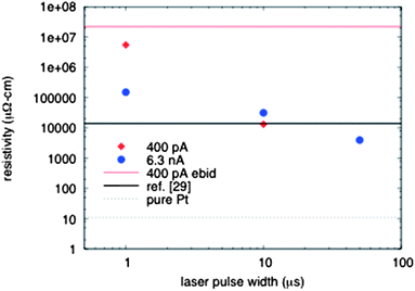 | ||
| Fig. 5 Measured resistivity from platinum EBID and LAEBID structures as a function of laser pulse width. | ||
To obtain a better understanding of what is occurring in the LAEBID process we performed Transmission Electron Microscopy (TEM) and Electron Energy Loss Spectroscopy (EELS) to investigate whether graphitization of the carbon matrix or a percolation network of platinum particles is forming during LAEBID resulting in significant reduction in deposit resistivity without an observable change in deposit platinum to carbon ratio. Thin EBID and LAEBID structures (∼10 nm thick) were deposited onto 15 nm SiNx membranes for TEM/EELS investigation. A short laser pulse width was used to prevent damage to the membrane, and thus comparisons using longer laser pulse widths could not be performed. Observations of the deposit structure with and without in situ laser treatment are made with a laser pulse width of 100 ns. Fig. 6 shows TEM images of (a) EBID and (b) LAEBID with a 100 ns pulse width at 186 kW cm−2. The two images shown here are shown at the same defocus for comparison. An obvious reduction in carbon and increase in the size of the Pt particles is occurring at the short laser pulse width. EELS measurements did not reveal graphitization in the 100 ns pulse width at 186 kW cm−2. Future work will investigate the change in carbon structure as a function of laser irradiance and pulse width in LAEBID materials.
 | ||
| Fig. 6 TEM images of (a) EBID and (b) LAEBID with a 100 ns pulse width. The dark regions are interpreted as the typical Pt nanoclusters in the amorphous carbon matrix. An obvious reduction in carbon and increase in the size of the Pt particles is occurring at the short laser pulse width. | ||
Finally, of critical importance to applications is the spatial resolution of the LAEBID process. Fig. 7 comparatively illustrates (a) standard EBID (5 keV, 400 pA, 100 μs dwell time, 1000 loops) and (b) LAEBID (10 μs, 186 kW cm−2) “spot” mode growth. As described previously the LAEBID vertical growth rate is slightly smaller, and importantly the lateral growth is also smaller and thus the LAEBID growths have ∼25% smaller pillar diameter in the single pixel dwell growth due to the removal of carbon and densification compared to the EBID growth. This enhanced resolution also confirms that thermal drift, which can be observed during continuous substrate heating methods, is not observed in the LAEBID process. Finally, compared to other post-deposition treatments, void formation and significant morphological defects are mitigated by the layer-by-layer process described here.
 | ||
| Fig. 7 SEM images of a single pixel dwell for (a) EBID and (b) LAEBID with a 10 μs pulse width. | ||
Conclusions
LAEBID enables the capability to create high purity EBID structures without creating porous structures (such as those obtained with ex situ thermal treatments) or thermally related structure distortion (with bulk substrate heating and cw laser heating). Optimized LAEBID conditions can also be minimally invasive, reactive, or destructive to the substrate making it an ideal process for creating localized, high purity nanomaterials for enhanced functionality. Future work will investigate further the electron and photon parameter space as well as the addition of a reactive gas such as oxygen to the chamber during LAEBID to deposit pure platinum nanostructures.Acknowledgements
The authors acknowledge that a portion of this research was conducted at the Center for Nanophase Materials Sciences, which is sponsored at Oak Ridge National Laboratory by the Scientific User Facilities Division, Office of Basic Energy Sciences, U.S. Department of Energy. Omniprobe acknowledges that the laser probe development was supported in part by the National Science Foundation under Small Business Innovation Research Grant # IIP-0956765 to Omniprobe, and under Grant # IIP-1059286 to the American Society for Engineering Education. The authors gratefully acknowledge J. Chen at CNMS for TEM imaging and C. M. Gonzalez at UT for electrical measurements.Notes and references
- M. G. Lassiter, T. Liang and P. D. Rack, J. Vac. Sci. Technol., B: Microelectron. Nanometer Struct.–Process., Meas., Phenom., 2008, 26, 963–967 CrossRef CAS.
- T. Liang, E. Frendberg, B. Lieberman and A. Stivers, J. Vac. Sci. Technol., B: Microelectron. Nanometer Struct.–Process., Meas., Phenom., 2005, 23, 3101–3105 CrossRef CAS.
- K. Edinger, H. Becht, J. Bihr, V. Boegli, M. Budach, T. Hofmann, H. W. P. Koops, P. Kuschnerus, J. Oster, P. Spies and B. Weyrauch, J. Vac. Sci. Technol., B: Microelectron. Nanometer Struct.–Process., Meas., Phenom., 2004, 22, 2902–2906 CrossRef CAS.
- Y. Guan, J. D. Fowlkes, S. T. Retterer, M. L. Simpson and P. D. Rack, Nanotechnology, 2008, 19, 505302 CrossRef.
- C. T. H. Heerkens, M. J. Kamerbeek, W. F. van Dorp, C. W. Hagen and J. Hoekstra, Microelectron. Eng., 2009, 86, 961–964 CrossRef CAS.
- F. Banhart, Nano Lett., 2001, 1, 329–332 CrossRef CAS.
- D. N. Madsen, K. Molhave, R. Mateiu, A. M. Rasmussen, M. Brorson, C. J. H. Jacobsen and P. Boggild, Nano Lett., 2003, 3, 47–49 CrossRef CAS.
- W. Ding, D. A. Dikin, X. Chen, R. D. Piner, R. S. Ruoff, E. Zussman, X. Wang and X. Li, J. Appl. Phys., 2005, 98, 4905–4911 CrossRef.
- T. Brintlinger, M. S. Fuhrer, J. Melngailis, I. Utke, T. Bret, A. Perentes, P. Hoffmann, M. Abourida and P. Doppelt, J. Vac. Sci. Technol., B: Microelectron. Nanometer Struct.–Process., Meas., Phenom., 2005, 23, 3174–3177 CrossRef CAS.
- J. H. Noh, M. Nikiforov, S. V. Kalinin, A. A. Vertegel and P. D. Rack, Nanotechnology, 2010, 21, 365302 CrossRef.
- N. A. Roberts, J. H. Noh, M. G. Lassiter, S. Guo, S. V. Kalinin and P. D. Rack, Nanotechnology, 2012, 23, 145301 CrossRef CAS.
- I. Utke, P. Hoffmann, R. Berger and L. Scandella, Appl. Phys. Lett., 2002, 80, 4792–4794 CrossRef CAS.
- A. Fernandez-Pacheco, J. M. De Teresa, R. Cordoba, M. R. Ibarra, D. Petit, D. E. Read, L. O'Brien, E. R. Lewis, H. T. Zeng and R. P. Cowburn, Appl. Phys. Lett., 2009, 94, 192509 CrossRef.
- L. Serrano-Ramon, R. Cordoba, L. A. Rodriguez, C. Magen, E. Snoeck, C. Gatel, I. Serrano, M. R. Ibarra and J. M. De Teresa, ACS Nano, 2011, 5, 7781–7787 CrossRef CAS.
- C. H. Schwalb, C. Grimm, M. Baranowski, R. Sachser, F. Porrati, H. Reith, P. Das, J. Muller, F. Volklein, A. Kaya and M. Huth, Sensors, 2010, 10, 9847–9856 CrossRef CAS.
- M. Weber, M. Rudolph, J. Kretz and H. W. P. Koops, J. Vac. Sci. Technol., B: Microelectron. Nanometer Struct.–Process., Meas., Phenom., 1995, 13, 461–464 CrossRef CAS.
- A. Perentes, A. Bachmann, M. Leutenegger, I. Utke, C. Sandu and P. Hoffmann, Microelectron. Eng., 2004, 73-74, 412–416 CrossRef CAS.
- P. Boggild, T. M. Hansen, C. Tanasa and F. Grey, Nanotechnology, 2001, 12, 331–335 CrossRef CAS.
- J. D. Fowlkes, M. J. Doktycz and P. D. Rack, Nanotechnology, 2010, 21, 5303–5311 CrossRef.
- N. Miura, H. Ishii, J.-I. Shirakashi, A. Yamada and M. Konagai, Appl. Surf. Sci., 1997, 113–114, 269–273 CrossRef.
- T. Mukawa, S. Okada, R. Kobayashi, J. Fujita, M. Ishida, T. Ichihashi, Y. Ochiai, T. Kaito and S. Matsui, Jpn. J. Appl. Phys., Part 1, 2005, 44, 5639–5640 CrossRef CAS.
- A. J. M. Mackus, J. J. L. Mulders, M. C. M. van de Sanden and W. M. M. Kessels, J. Appl. Phys., 2010, 107, 116102 CrossRef.
- S. J. Randolph, J. D. Fowlkes and P. D. Rack, Crit. Rev. Solid State Mater. Sci., 2006, 31, 55–89 CrossRef CAS.
- I. Utke, P. Hoffmann and J. Melngailis, J. Vac. Sci. Technol., B: Microelectron. Nanometer Struct.–Process., Meas., Phenom., 2008, 26, 1197–1276 CrossRef CAS.
- W. F. v. Dorp and C. W. Hagen, J. Appl. Phys., 2008, 104, 1301–1342 Search PubMed.
- A. Fernandez-Pacheco, J. M. De Teresa, R. Cordoba and M. R. Ibarra, J. Phys. D: Appl. Phys., 2009, 42, 055005 CrossRef.
- K. L. Klein, S. J. Randolph, J. D. Fowlkes, L. F. Allard, H. M. Meyer III, M. L. Simpson and P. D. Rack, Nanotechnology, 2008, 19, 345705 CrossRef.
- V. Gopal, V. R. Radilovic, C. Daraio, S. Jin, P. Yang and E. A. Stach, Nano Lett., 2004, 4, 2059–2063 CrossRef CAS.
- A. Botman, J. J. L. Mulders, R. Weemaes and S. Mentink, Nanotechnology, 2006, 17, 3779–3785 CrossRef CAS.
- R. M. Langford, T. X. Wang and D. Ozkaya, Microelectron. Eng., 2007, 84, 784–788 CrossRef CAS.
- R. Cordoba, J. Sese, J. M. De Teresa and M. R. Ibarra, Microelectron. Eng., 2010, 87, 1550–1553 CrossRef CAS.
- J. J. L. Mulders, L. M. Belova and A. Riazanova, Nanotechnology, 2011, 22, 055302 CrossRef CAS.
- A. Botman, M. Hesselberth and J. J. L. Mulders, Microelectron. Eng., 2008, 85, 1139–1142 CrossRef CAS.
- H. Plank, C. Gspan, M. Dienstleder, G. Kothleitner and F. Hofer, Nanotechnology, 2008, 19, 485302 CrossRef CAS.
- R. M. Langford, D. Ozkaya, J. Sheridan and R. Chater, Microsc. Microanal., 2004, 10, 1122–1123 CrossRef.
- S. Wang, Y.-M. Sun, Q. Wang and J. M. White, J. Vac. Sci. Technol., B: Microelectron. Nanometer Struct.–Process., Meas., Phenom., 2004, 22, 1803–1806 CrossRef CAS.
- M. H. Ervin, D. Chang, B. Nichols, A. Wickenden, J. Barry and J. Melngailis, J. Vac. Sci. Technol., B: Microelectron. Nanometer Struct.–Process., Meas., Phenom., 2007, 25, 2250–2254 CrossRef CAS.
- M. Takeguchi, M. Shimojo and K. Furuya, Appl. Phys. A, 2008, 93, 439–442 CrossRef CAS.
- S. Frabboni, G. C. Gazzadi, L. Felisari and A. Spessot, Appl. Phys. Lett., 2006, 88, 213116 CrossRef.
- F. Porrati, R. Sachser, C. H. Schwalb, A. S. Frangakis and M. Huth, J. Appl. Phys., 2011, 109, 063715 CrossRef.
- A. Botman, J. J. L. Mulders and C. W. Hagen, Nanotechnology, 2009, 20, 372001 CrossRef CAS.
- J. Funatsu, C. V. Thompson, J. Melngailis and J. N. Walpole, J. Vac. Sci. Technol., B: Microelectron. Nanometer Struct.–Process., Meas., Phenom., 1996, 14, 179–180 CrossRef CAS.
- N. A. Roberts, G. A. Magel, C. D. Hartfield, T. M. Moore, J. D. Fowlkes and P. D. Rack, J. Vac. Sci. Technol., A, 2012, 30, 041404 Search PubMed.
- D. Burgess, P. C. Stair and E. Weitz, J. Vac. Sci. Technol., A, 1985, 4, 1362–1366 Search PubMed.
- H. Plank, G. Kothleitner, F. Hofer, S. G. Michelitsch, C. Gspan, A. Hohenau and J. Krenn, J. Vac. Sci. Technol., B: Nanotechnol. Microelectron.: Mater., Process., Meas., Phenom., 2011, 29, 051801 Search PubMed.
- J. D. Wnuk, J. M. Gorham, S. G. Rosenberg, W. F. v. Dorp, T. E. Madey, C. W. Hagen and D. H. Fairbrother, J. Phys. Chem., 2009, 113, 2487–2496 CAS.
- H. Plank, D. A. Smith, T. Haber, P. D. Rack and F. Hofer, ACS Nano, 2012, 6, 286–294 CrossRef CAS.
- V. Friedli, C. Santschi, J. Michler, P. Hoffmann and I. Utke, Appl. Phys. Lett., 2007, 90, 053106 CrossRef.
- J. Puretz and L. W. Swanson, J. Vac. Sci. Technol., B: Microelectron. Nanometer Struct.–Process., Meas., Phenom., 1992, 10, 2695–2698 CrossRef CAS.
- P. F. A. Alkemade, H. Miro, E. v. Veldhoven, D. J. Maas, D. A. Smith and P. D. Rack, J. Vac. Sci. Technol., B: Nanotechnol. Microelectron.: Mater., Process., Meas., Phenom., 2011, 29, 06FG05 Search PubMed.
- K. T. Kohlmann, M. Thiemann and W. H. Brunger, Microelectron. Eng., 1991, 13, 279–282 CrossRef CAS.
- J. D. Fowlkes, S. J. Randolph and P. D. Rack, J. Vac. Sci. Technol., B: Microelectron. Nanometer Struct.–Process., Meas., Phenom., 2005, 23, 2825 CrossRef CAS.
- D. A. Smith, J. D. Fowlkes and P. D. Rack, Nanotechnology, 2007, 18, 265308 CrossRef CAS.
- J. D. Fowlkes and P. D. Rack, ACS Nano, 2010, 4, 1619–1629 CrossRef CAS.
- D. A. Smith, J. D. Fowlkes and P. D. Rack, Nanotechnology, 2008, 19, 415704 CrossRef.
- I. Utke, V. Friedli, M. Purrucker and J. Michler, J. Vac. Sci. Technol., A, 2007, 25, 2219 CAS.
Footnote |
| † Electronic supplementary information (ESI) available: Additional information regarding the finite element simulation, electrical measurements and post-process annealing is available. See DOI: 10.1039/c2nr33014h |
| This journal is © The Royal Society of Chemistry 2013 |