Hierarchical TiO2 microspheres comprised of anatase nanospindles for improved electron transport in dye-sensitized solar cells
Dapeng
Wu
ab,
Yi
Wang
c,
Hui
Dong
b,
Feng
Zhu
b,
Shuyan
Gao
a,
Kai
Jiang
*a,
Limin
Fu
*c,
Jianping
Zhang
c and
Dongsheng
Xu
*b
aSchool of Chemistry and Chemical Engineering, Henan Key Laboratory of Photovoltaic Materials, Henan Normal University, Henan Xinxiang 453007, P.R. China. E-mail: jiangkai6898@126.com; Fax: +86-37-3326209; Tel: +86-37-3326209
bBeijing National Laboratory for Molecular Sciences, State Key Laboratory for Structural Chemistry of Unstable and Stable Species, College of Chemistry and Molecular Engineering, Peking University, Beijing 100871, P.R. China. E-mail: dsxu@pku.edu.cn; Fax: +86-10-62760360; Tel: +86-10-62760360
cDepartment of Chemistry, Renmin University of China, Beijing 100872, P.R. China. E-mail: lmfu@chem.ruc.edu.cn; Fax: +86-10-62511528; Tel: +86-10-62511528
First published on 5th November 2012
Abstract
Hierarchical TiO2 microspheres assembled by nanospindles were prepared via a two-step hydrothermal method. The as-prepared products have uniform diameters of ∼450 nm and surface area of ∼88 m2 g−1. The optical investigation evidenced that the photoanode film has a prominent light scattering effect at a wavelength range of 600–800 nm and possesses enhanced dye loading capacity. In addition, the electron recombination and transport dynamic measurements indicated that these hierarchical products could suppress the recombination and improve the diffusion coefficient of the photoelectrons, which can be attributed to the improvement of the connectivity by bridging the neighbouring microspheres through the embedded nanospindles. As a result, a high power conversion efficiency of 8.5% was demonstrated, indicating a ∼30% improvement compared with the cell derived from the well-defined nanocrystalline microspheres (6.5%).
1 Introduction
Dye-sensitized solar cells (DSSCs) have been intensively studied in the past two decades because of their low cost, high efficiency and facile preparation process.1–3 Various TiO2 structures such as nanoparticles,4,5 nanorods/wires,6–9 nanotube arrays,10–14 mesoporous beads15,16 and hollow spheres17–20 have been proposed as photoanode materials to optimize the performance of the device. Heretofore, high power conversion efficiencies (PCEs) of more than 11% have been demonstrated by the TiO2-based cells.21,22In a working DSSC, the monolayer dye molecules attached to the surface of the wideband gap semiconductor nanocrystallines (e.g. TiO2) firstly harvest the incident light to generate free excited electrons. Afterwards, the photoinduced electrons are injected into the conduction band of the semiconductor and collected by the photoanode substrate (e.g. fluorine doped SnO2 (FTO) glass). The as-collected photoelectrons are finally transported to the external load and generate photocurrent. Generally, the high surface area, good light scattering capacity and fast electron transport were considered as the foremost requirements for an ideal photoanode material.23,24
TiO2 hierarchical microspheres (HMSs) with high surface area and compatible diameters were deliberately introduced as bi-functional candidates to mediate the competition between the dye loading amount and scattering effect of the photoanode.25,26 Caruso et al. firstly prepared mesoporous anatase TiO2 beads with high surface area and submicron sized diameter to enhance the light harvesting within the photoanode.15,27 However, most of the reported hierarchical microspheres were virtually composed of nanocrystallines and the numerous grain boundaries brought forth many recombination opportunities between the photoelectrons and the electron acceptors. Recently, TiO2 HMSs assembled by oriented attached nanocrystals have been demonstrated to improve the interparticle connection and then enhance the charge transport in the film.28 Although the microspheres with particularly designed subunits could improve the electron transport within an individual microsphere,29,30 the small contact area among the neighbouring microspheres could reduce the connectivity of the nanoporous film and impact the electron transport across the photoanode. To improve the film connectivity, TiO2 nanocrystallines were intentionally introduced in the microspheres to fill the voids existing in the photoanode film.31 However, the added nanocrystallines might increase the number of grain boundaries and promote the electron recommendation rate.
Herein, we designed and prepared TiO2 HMSs embedded with nanospindles to promote the electron transport by bridging the neighbouring microspheres within the photoanode. The as-prepared product is ∼450 nm in diameter and has a surface area of ∼88 cm2 g−1. Therefore, it could serve as a good candidate offering high dye loading capacity and prominent scattering effect, which leads to effective harvesting of the incident light. In addition, based on the transient photovoltage and photocurrent investigation, the product embedded with highly crystallized nanospindles could suppress the recombination and promote the diffusion coefficient of the photoelectrons. As a result, a higher conversion efficiency of 8.5% was demonstrated, indicating a ∼30% improvement compared with the cell derived from the well-defined nanocrystalline HMSs (6.5%).
2 Experimental section
2.1 Sample preparation
0.65 g of P25 (Degussa) was dispersed in a mixture solution of 87.5 mL of hydrogen peroxide (H2O2, 30 wt%) and 12.5 mL of ammonia (NH4OH, 26–28 wt%). After being stirred at room temperature for 24 h, the suspension was converted to a clear light yellow solution. Afterwards, 20 mL of the yellow precursor was extracted and transferred into a 100 mL Teflon container, with addition of 20 mL of distilled water and 40 mL of absolute ethanol. The mixture was then sealed tightly with a stainless jacket and heated at 160 °C for 30 min and 6 h to obtain the intermediate products: precursor A and precursor B. Subsequently, 0.15 g of precursor A and precursor B were respectively dispersed in 40 mL of distilled water and sealed in a 50 mL Teflon-lined autoclave. The suspensions were treated at 180 °C for different times: precursor A for 6 h and precursor B for 3 h. After being centrifuged and washed with water and ethanol, the final products were obtained and denoted as well-defined HMSs and nanospindle-embedded HMSs.2.2 Fabrication of the DSSCs
To prepare the paste, hydroxypropyl cellulose (Aldrich) was added to diethylene glycol with a concentration of ∼10 wt%. The paste was added into the obtained microspheres with a ratio of ∼40 wt% of TiO2. After vigorous stirring, a homogeneous slurry was prepared. Before depositing the main layer by a doctor-blade method, a ∼100 nm blocking layer composed of TiO2 nanocrystallines (15–20 nm) was firstly constructed onto the fluorine-doped tin oxide (FTO) glass substrate (TEC-8, LOF). After being dried in air, the films were heated up to 450 °C with a rate of 5 °C min−1 and maintained for 30 min. The film thicknesses were all controlled at ∼14 μm. After being cooled to 80 °C, the films were sensitized in a solution of cis-bis(isothiocyanato)bis(2,2′-bipyridy1-4,4′-dicarboxylate) ruthenium(II)bis-tetrabutylammonium (N719, Solaronix SA, Switzerland) in ethanol (3 × 10⁻⁴ M) for 24 h. The dyed films were then sandwiched together with platinized FTO counter electrodes and electrolyte was then injected into the cell from the edges by capillarity. The content of the electrolyte is 0.05 M LiI, 0.03 M I2, 0.5 M tert-butylpyridine, 0.1 M GuNCS and 1 M BMII in a solvent mixture of 85% acetonitrile and 15% valeronitrile.2.3 Material characterizations
The morphologies and structures of the products were characterized by field-emission scanning electron microscopy (FESEM, HITACHI, S4800), transmission electron microscopy (TEM, FEI Tecnai F30), X-ray powder diffraction (XRD, Rigaku D/max-2500 diffractometer with Cu Kα radiation, λ = 0.1542 nm, 40 kV, 100 mA) and Brunauer–Emmett–Teller (BET, Micrometrics ASAP 2010).2.4 Photovoltage measurements
Photocurrent–voltage (I–V) measurements were performed on a Keithley 4200 semiconductor characterization system using a simulated AM 1.5 sunlight with an output power of 100 mW cm−2 produced by a solar simulator (Newport 69911). The active area was controlled by scratching off the excessive film leaving a 0.4 cm × 0.4 cm film area on the FTO. The cells were placed 25 cm away from the light source and illuminated from the front side.Incident monochromatic photo-to-electron conversion efficiency (IPCE) was recorded on a Keithley 2000 source meter under the irradiation of a 150 W tungsten lamp with a 1/4 m monochromator (Spectral Product DK240). The optical diffuse-reflection spectra were measured using a spectrophotometer (HITACHI U-4100).
2.5 Photovoltage and photocurrent transient measurements
In the transient measurements, two light emitting diodes (LED, 530 nm) were used as the bias light source to generate the steady voltages and the pulse excitation light source to produce transient signals. Light from these two LEDs was collected by two identical lens groups and imaged on the DSSC surface with a spot size of ∼8 mm × 8 mm. The bias light intensity could be adjusted from 1 μW to 60 mW by a DC regulated power supply to generate different steady open circuit voltages. The pulse light LED was driven by a self-made pulse amplifier and the excitation light intensity was set as 2 μJ per pulse with a duration of 50 μs. The photovoltage transients under different steady bias voltages were directly recorded using an oscilloscope (Lecroy 64Xs) with an input resistance of 1 MΩ. The photocurrent transients under different bias voltages were recorded using an oscilloscope with an input resistance of 50 Ω and shunted with a 50 Ω series resistor. Moreover, a current amplifier (Stanford Research Systems, SR445A) was also incorporated in front of the oscilloscope. The as-obtained photovoltage and photocurrent decay curves were fitted by Matlab 7.0 with an exponential function of y = y0 + A1exp(−x/t1) + A2exp(−x/t2), where y0 is the baseline, A1 and A2 are the pre-exponential factors, t1 and t2 are the time constants. Afterwards, the recombination lifetime (τr) and the collection time (τc) are calculated according to the equation τ = (A1t1 + A2t2)/(A1 + A2).3 Results and discussion
3.1 Morphological and structural characterizations
Fig. 1a and b display the intermediate products collected at 30 min and 6 h in the first step of solvothermal reaction (denoted as precursor A and precursor B). Precursor A is mainly composed of uniform microspheres with a diameter of ∼500 nm. With increasing reaction time to 6 h, large nanospindles were found to distribute on the microspheres in precursor B. Fig. 1c and d show the samples after hydrothermal conversion at 180 °C, which are respectively labeled as well-defined (WD) HMSs and nanospindle-embedded (NSE) HMSs. The well-defined HMSs are composed of microspheres with uniform diameter of ∼450 nm. Moreover, the HMSs are solely assembled by nanosized particles.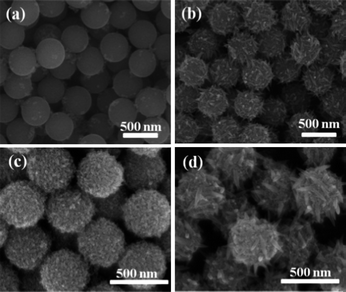 | ||
| Fig. 1 SEM images of the intermediate samples (a) precursor A and (b) precursor B; and the samples after hydrothermal conversion (c) the well-defined HMSs and (d) the nanospindle-embedded HMSs. | ||
The nanospindle-embedded HMSs are of similar outer diameter but embedded with many large nanospindles. The corresponding TEM images displayed in Fig. 2a and b confirm that the well-defined HMSs are aggregated by the nanocrystallines which are 20–30 nm in length and ∼10 nm in width. The TEM image displayed in Fig. 2c depicts that the large nanospindles embedded in the HMSs are about 100–200 nm in length and 20–30 nm in diameter. Moreover, as displayed in Fig. 2d, the interplanar spacings of the large nanospindles are measured to be 0.35 and 0.48 nm respectively, indicating that the nanospindles are growing along the 〈001〉 direction. The inset fast Fourier transfer (FFT) image further proves the single crystal nature and growth direction of the spindle.
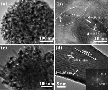 | ||
| Fig. 2 TEM images of (a and b) the well-defined HMSs and (c and d) the nanospindle-embedded HMSs. The inset of (d) is the corresponding FFT image. | ||
As depicted in Fig. 3, the crystallographic structures of the as-prepared samples are confirmed by X-ray diffraction (XRD). No obvious diffraction peak is found in precursor A, indicating that the firstly formed microspheres are amorphous. Weak diffraction peaks indexed to anatase TiO2 (JCDPS no. 21-1271) are detected in precursor B, suggesting that the later generated large nanospindles are anatase phase. After the second step of hydrothermal conversion, the nanospindle-embedded HMSs exhibit stronger diffraction peaks than the well-defined HMSs, suggesting that they have better crystal quality. Moreover, the nanospindle-embedded HMSs have a sharper and stronger (004) peak compared with other samples, which confirms that the evolution of the large nanospindles is along the 〈001〉 direction.32
 | ||
| Fig. 3 XRD patterns of the as-prepared products: (a) precursor A, (b) precursor B, (c) the well-defined HMSs and (d) the nanospindle-embedded HMSs. | ||
Fig. 4 shows the nitrogen adsorption–desorption isotherm measurements of the HMSs. The isotherm displays the typical type IV curve with a H3 hysteresis. Moreover, compared with the well-defined HMSs, nanospindle-embedded HMSs have a suppressed loop in the high pressure area indicating the existence of larger pores.33 The Brunauer–Emmett–Teller (BET) surface area of the well-defined and nanospindle-embedded HMSs is ∼101.6 and ∼88.7 m2 g−1, respectively. Meanwhile, the inset pore-size distribution curve indicates that the nanospindle-embedded HMSs have a greater and wider pore size distribution (centred at ∼18.9 nm) than the well-defined HMSs (centred at ∼11.7 nm).
 | ||
| Fig. 4 Nitrogen adsorption–desorption isotherm of the well-defined and nanospindle-embedded HMSs. The inset is the corresponding Barret–Joyner–Halenda (BJH) pore size distribution plots. | ||
3.2 Photovoltage performance
The well-defined and nanospindle-embedded HMSs were deposited as DSSC photoanode films which are denoted as Film-WD and Film-NSE, respectively. Fig. 5a and c reveal the SEM images of the film cross-section, indicating that the films are homogenously deposited on the FTO substrate with a thickness of ∼14 μm. Fig. 5b shows the magnified image of Film-WD. The well-defined HMSs leave large voids in the film, indicating a poor connectivity among the neighbouring microspheres. For Film-NSE, as displayed in Fig. 5d, the neighbouring microspheres are inclined to melt together to form a closely linked network. As illustrated in Scheme 1a, the deposition of well-defined HMSs spontaneously results in large voids in the photoanode, which would lead to low connectivity among the microspheres. In contrast, as shown in Scheme 1b, the large nanospindles embedded in the HMSs could link the neighbouring microspheres as bridges and thus the film possesses a relatively higher packing density. Meanwhile, in the same film thickness, the number of the HMSs in Film-NSE should be larger than that in Film-WD. As a result, although the nanospindle-embedded HMSs have a lower specific surface area, Film-NSE exhibits relatively higher dye loading capacity (Table 1). | ||
| Fig. 5 SEM images of the film cross-sections: (a) the overall and (b) magnified view of Film-WD; (c) the overall and (d) the magnified view of Film-NSE. | ||
 | ||
| Scheme 1 Illustration of the structures of (a) Film-WD and (b) Film-NSE. | ||
| Cells | J sc/mA cm−2 | V oc/mV | FF/% | PCE/% | Dye absorption/mol cm−2 |
|---|---|---|---|---|---|
| WD-HMSs | 14.8 | 732 | 59.9 | 6.5 | 2.2 × 10⁻⁷ |
| NSE-HMSs | 16.3 | 766 | 68.2 | 8.5 | 2.4 × 10⁻⁷ |
The DSSCs derived from the well-defined and nanospindle-embedded HMSs were denoted as Cell-WD and Cell-NSE. Fig. 6 shows the typical current density versus voltage (I–V) curves of the DSSCs, and the detailed cell performance is summarized in Table 1. Cell-WD reveals a current density (Jsc), open-circuit voltage (Voc) and fill factor (FF) of 14.8 mA cm−2, 732 mV and 59.5%, respectively. As a result, the PCE reaches 6.5%. Conspicuously, Cell-NSE demonstrates a much higher Jsc of 16.3 mA cm−2, Voc of 766 mV and FF of 68.2%. As a result, the PCE of Cell-NSE is enhanced to 8.5%, which indicates a ∼30% improvement compared with that of Cell-WD. It is obvious that the PCE enhancement results from the synergistic increase of the Jsc, Voc and FF. The shape of the I–V curve of Cell-WD shows a gentler slope at the higher voltage region compared with that of Cell-NSE. Commonly, the inversed slope at the higher voltage region indicates the variation of the series resistances of the cells, which is related to the resistances of both the semiconductor film and the ohmic contact of metal components in testing.34 Similarly, we also believe that the low FF of Cell-WD may be caused by the high series resistance in the semiconductor film due to the poor connectivity between the HMSs.
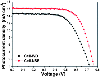 | ||
| Fig. 6 The current–voltage characteristics of the as-prepared DSSCs, measured under one sun (AM 1.5G, 100 mW cm−2). | ||
Fig. 7 displays the UV-vis reflectance spectra of the films. Different from the nanocrystalline films that usually exhibit high transparency in the visible range, all the HMS-based films have high reflectance in the range of 400–800 nm. The inset diagram shows that Film-WD exhibits two characteristic peaks located at ∼550 and ∼725 nm, respectively. It is evident that the centre of the main peak of Film-NSE is blue shifted from ∼725 nm to ∼675 nm. As we know, the photonic peaks in the reflection curves of HMS-based photoanode films indicate the intensification of the scattering and closely depend on the size distribution of the HMSs.20,35 With an increase of the diameter of the HMSs, the intensity of the reflection curves would be enhanced and the peak position of the photonic peak might be red-shifted. Although the two types of HMSs have similar outer diameters, the sprouting nanospindles at the outer area of the nanospindle-embedded HMSs may have lower scattering ability than the inner part with high density (inset illumination in Fig. 7). Therefore, the effective diameter of the HMSs for scattering is reduced in Film-NSE, resulting in a blue-shift of the photonic peaks and a slight decrease in scattering intensity.36
 | ||
| Fig. 7 The UV-vis reflectance spectra of the as-prepared films. The inset diagram shows the photonic reflection peaks by subtracting the corresponding reflection curves, and the inset illustration presents the difference between the effective diameters of the HMSs. | ||
Fig. 8 shows the incident monochromatic photo-to-electron conversion efficiency (IPCE) spectra as a function of wavelength for the cells. Cell-NSE possesses higher IPCE values at the whole spectrum compared with Cell-WD. In addition, the two DSSCs all exhibit broad and clear IPCE peaks in the range of 600–700 nm, which probably results from the good scattering effect of the submicron-sized HMSs. The IPCE of DSSCs is determined by the light harvesting efficiency of the film (ηlh), the injection (ηinj) and collection efficiencies (ηcol) of the photoelectrons, which are generally affected by the structure of the photoelectrode (eqn (1)).37,38
| ηIPCE = ηlhηinjηcol | (1) |
 | ||
| Fig. 8 The IPCE spectra of the as-prepared DSSCs. | ||
Although Film-NSE possesses a slightly reduced scattering effect, the improvement in dye loading capacity could compensate the loss in the ηlh. Moreover, the good connectivity of the HMSs may also improve the ηcol, which finally leads to an improved IPCE value at the whole spectrum range.
3.3 Electron recombination and transport dynamics
In order to further interpret the electron recombination and transport dynamics, the cells were tested by the transient photovoltage and photocurrent measurements. The in situ electron recombination lifetime (τr) could be measured at the open circuit conditions, in which the injected photoelectrons would all recombine with the redox spices at the TiO2/dye/electrolyte interface and result in an exponential decay of the photovoltage.39 The τr is therefore estimated by the exponential fitting of the photovoltage transient decay curves. Fig. 9 depicts the τr obtained at different bias voltages for the two cells. Generally, the charge recombination kinetics can be divided into three sections: the free electrons from the conduction band energy level to the electron acceptors in the electrolyte, the electrons from shallow traps to the acceptors and the electrons from the deep traps to the acceptors.40,41 In our case, the bias voltage induced by applying steady illumination could fill electrons into the energy levels with a sequence of deep traps, shallow traps and the conduction band. By increasing the bias voltage, more trap states have been filled and the pulse illumination generated photoelectrons are injected into the higher energy levels, which induce a faster recombination when the pulse illumination is cut off. As a result, the as-measured τr value should decrease (Fig. 9). Meanwhile, Cell-NSE has a larger τr than that of Cell-WD at the whole voltage range, implying that the charge recombination between the injected photoelectrons and the electron acceptors in Film-NSE is retarded. The suppressed recombination of the charge carriers would increase the electron density in the conduction band of the TiO2 framework, elevate the quasi-Fermi energy level, and result in the enhancement of the Voc of Cell-NSE.42,43 | ||
| Fig. 9 The electron recombination lifetime (τr) of the DSSCs measured under different bias voltages for the as-prepared DSSCs. | ||
Fig. 10 displays the collection time (τc) of the photoelectron as a function of the bias voltages. Here, τc could be determined by fitting the exponential decay curve of the photocurrent appeared on cutting off the pulse illumination. It is obvious that Cell-NSE has evident lower τc at the whole bias voltage range, indicating that the photoelectrons could be more effectively transported to the substrate compared with Cell-WD. Moreover, the electron effective diffusion coefficient (De) could be calculated based on the equation De = d2/2.35τc, where d is the film thickness and τc is the collection time obtained as no bias voltage was applied (0 V).44 As a result, Cell-NSE shows a higher De of 16.2 × 10⁻⁹ m2 s−1 which is almost three times the value of Cell-WD (6.7 × 10⁻⁹ m2 s−1). It is reasonable that the large nanospindles embedded in HMSs could bridge the adjacent microspheres to improve their connectivity and consequently results in an increase of the electron transport efficiency. In addition, we found that all the curves are relatively flat at the potential region of 0–600 mV and the τc experiences a rapid growth at the potential above 600 mV. In general, the electron diffusion rate depends on the competition between the De and the electron concentration gradient. By increasing the bias voltage, an increase of the De would be accompanied by a decrease of the electron concentration gradient, which leads to the small variation of the τc values. However, when the bias voltage increases close to the conduction band, the potential gradient may abruptly decrease due to the free electron exchanging between the approaching energy levels. As a result, the electron diffusion is retarded and the as-measured τc value is enhanced accordingly.
 | ||
| Fig. 10 The collection times (τc) of the DSSCs measured under different bias voltages for the as-prepared DSSCs. | ||
4 Conclusion
In summary, anatase TiO2 microspheres embedded with nanospindles were prepared via a two-step hydrothermal method. The as-prepared microspheres are ∼450 nm in diameter and possess a surface area of ∼88 m2 g−1. The DSSC derived from the nanospindle-embedded HMSs shows a high conversion efficiency of 8.5% accompanied by a Jsc of 16.3 mA cm−2, Voc of 766 mV and FF of 68.2%, which demonstrates a ∼30% PCE improvement compared to Cell-WD. Moreover, the embedded high quality nanospindles could bridge the neighbouring microspheres and enhance the connectivity of the film. Therefore, a longer electron recombination lifetime and higher electron diffusion coefficient were detected in Cell-NSE. Finally, with these unique structural advantages, the TiO2 HMSs as photoanode frameworks could find potential applications in other solar energy conversion devices.Acknowledgements
This work is supported by NSFC (Grant no. 20903117, 20933010, 51121091, 21133001, 61204078 and 61176004), MSTC (Grant no. 2011CB808702), and the Research Funds of Renmin University of China (no. 10XNI007).Notes and references
- B. O'Regan and M. Gratzel, Nature, 1991, 353, 737 CrossRef CAS.
- M. Gratzel, Nature, 2001, 414, 338 CrossRef CAS.
- M. Gratzel, Inorg. Chem., 2005, 44, 6841 CrossRef.
- C. J. Barbe, F. Arendse, P. Comte, M. Jirousek, F. Lenzmann, V. Shklover and M. Gratzel, J. Am. Ceram. Soc., 1997, 80, 3157 CrossRef CAS.
- K. Fan, C. Gong, T. Peng, J. Chen and J. Xia, Nanoscale, 2011, 3, 3900 RSC.
- R. Buonsanti, E. Carlino, C. Giannini, D. Altamura, L. De Marco, R. Giannuzzi, M. Manca, G. Gigli and P. D. Cozzoli, J. Am. Chem. Soc., 2011, 133, 19216 CrossRef CAS.
- M. Adachi, Y. Murata, J. Takao, J. Jiu, M. Sakamoto and F. Wang, J. Am. Chem. Soc., 2004, 126, 14943 CrossRef CAS.
- P. Poudel and Q. Qiao, Nanoscale, 2012, 4, 2826 RSC.
- D. Roh, R. Patel, S. Ahn, D. Kim and J. Kim, Nanoscale, 2011, 3, 4162 RSC.
- M. Paulose, K. Shankar, O. K. Varghese, G. K. Mor, B. Hardin and C. A. Grimes, Nanotechnology, 2006, 17, 1446 CrossRef CAS.
- Q. W. Chen and D. S. Xu, J. Phys. Chem. C, 2009, 133, 6310 Search PubMed.
- Q. W. Chen, D. S. Xu, Z. Y. Wu and Z. F. Liu, Nanotechnology, 2008, 19, 365708 CrossRef.
- C. Yip, M. Guo, H. Huang, L. Zhou, Y. Wang and C. Huang, Nanoscale, 2012, 4, 448 RSC.
- P. Roy, D. Kim, K. Lee, E. Spiecker and P. Schmuki, Nanoscale, 2010, 2, 45 RSC.
- D. H. Chen, F. Z. Huang, Y. B. Cheng and R. A. Caruso, Adv. Mater., 2009, 21, 2206 CrossRef CAS.
- D. H. Chen, L. Cao, F. Z. Huang, P. Imperia, Y. B. Cheng and R. A. Caruso, J. Am. Chem. Soc., 2010, 132, 4438 CrossRef CAS.
- H. J. Koo, Y. J. Kim, Y. H. Lee, W. Lee, K. Kim and N. G. Park, Adv. Mater., 2008, 20, 195 CrossRef CAS.
- X. Wu, G. Q. (Max) Lu and L. Z. Wang, Energy Environ. Sci., 2011, 4, 3565 CAS.
- J. F. Qian, P. Liu, Y. Xiao, Y. Jiang, Y. Cao, X. P. Ai and H. X. Yang, Adv. Mater., 2009, 21, 3663 CrossRef CAS.
- D. Wu, F. Zhu, L. Li, H. Dong, Q. Li, K. Jiang and D. Xu, J. Mater. Chem., 2012, 22, 11665 RSC.
- M. K. Nazeeruddin, F. De Angelis, S. Fantacci, A. Selloni, G. Viscardi, P. Liska, S. Ito, B. Takeru and M. G. Gratzel, J. Am. Chem. Soc., 2005, 127, 16835 CrossRef CAS.
- A. Yella, H. W. Lee, H. N. Tsao, C. Yi, A. K. Chandiran, M. K. Nazeeruddin, E. W. G. Diau, C. Y. Yeh, S. M. Zakeeruddin and M. Gratzel, Science, 2011, 334, 629 CrossRef CAS.
- Q. F. Zhang, T. P. Chou, B. R. Russo, S. A. Jenekhe and G. Z. Cao, Angew. Chem., Int. Ed., 2008, 47, 2402 CrossRef CAS.
- L. D. Marco, M. Manca, R. Buonsanti, R. Giannuzzi, F. Malara, P. Pareo, L. Martiradonna, N. M. Giancaspro, P. D. Cozzolibc and G. Gigli, J. Mater. Chem., 2011, 21, 13371 RSC.
- W. G. Yang, J. M. Li, Y. Wang, F. Zhu, W. Shi, F. R. Wan and D. S. Xu, Chem. Commun., 2011, 47, 1809 RSC.
- F. Sauvage, D. H. Chen, P. Comte, F. Z. Huang, L. P. Heiniger, Y. B. Cheng, R. A. Caruso and M. Graetzel, ACS Nano, 2010, 4, 4420 CrossRef CAS.
- F. Z. Huang, D. H. Chen, X. L. Zhang, R. A. Caruso and Y. B. Cheng, Adv. Funct. Mater., 2010, 20, 1301 CrossRef CAS.
- W. G. Yang, F. R. Wan, Q. W. Chen, J. J. Li and D. S. Xu, J. Mater. Chem., 2010, 20, 2870 RSC.
- J. Y. Liao, B. X. Lei, D. B. Kuang and C. Y. Su, Energy Environ. Sci., 2011, 4, 4079 CAS.
- Y. J. Kim, M. H. Lee, H. J. Kim, G. Lim, Y. S. Choi, N. G. Park, K. Kim and W. Lee, Adv. Mater., 2009, 21, 3668 CrossRef CAS.
- J. Xi, Q. Zhang, K. Parka, Y. Sun and G. Cao, Electrochim. Acta, 2011, 56, 1960 CrossRef CAS.
- C. Dinh, T. Nguyen, F. Kleitz and T. Do, ACS Nano, 2009, 3, 3737 CrossRef CAS.
- J. G. Yu and J. Zhang, Dalton Trans., 2010, 39, 5860 RSC.
- M. Kim, B. Kim and J. Kim, ACS Appl. Mater. Interfaces, 2009, 6, 1264 Search PubMed.
- F. Zhu, D. Wu, F. Zhu, Q. Li, H. Dong, J. Li, K. Jiang and D. Xu, RSC Adv., 2012, 2, 11629 RSC.
- I. Yu, Y. Kim, H. Kim, C. Lee and W. I. Lee, J. Mater. Chem., 2011, 21, 532 RSC.
- N. G. Park, J. van de Lagemaat and A. J. Frank, J. Phys. Chem. B, 2000, 104, 8989 CrossRef CAS.
- M. K. Nazeeruddin, A. Kay, I. Rodicio, R. Humphry-Baker, E. Mueller, P. Liska, N. Vlachopoulos and M. Gratzel, J. Am. Chem. Soc., 1993, 115, 6382 CrossRef CAS.
- F. Zhu, P. Zhang, X. Wu, L. Fu, J. Zhang and D. Xu, ChemPhysChem, 2012, 13, 3731 CrossRef CAS.
- J. Bisquert, A. Zaban, M. Greenshtein and I. Mora-Sero, J. Am. Chem. Soc., 2004, 126, 13550 CrossRef CAS.
- J. Bisquert, F. Fabregat-Santiago, I. Mora-Sero, G. Garcia-Belmonte and S. Gimenez, J. Phys. Chem. C, 2009, 113, 17278 CAS.
- S. Y. Huang, G. Schlichthorl, A. J. Nozik, M. Gratzel and A. J. Frank, J. Phys. Chem. B, 1997, 101, 2576 CrossRef CAS.
- G. Boschloo and A. Hagfeldt, Acc. Chem. Res., 2009, 42, 1819 CrossRef CAS.
- J. van de Lagemaat and A. J. Frank, J. Phys. Chem. B, 2001, 105, 11194 CrossRef CAS.
| This journal is © The Royal Society of Chemistry 2013 |