Oxygen and light sensitive field-effect transistors based on ZnO nanoparticles attached to individual double-walled carbon nanotubes†
Alina
Chanaewa
a,
Beatriz H.
Juárez
b,
Horst
Weller
a and
Christian
Klinke
*a
aInstitute of Physical Chemistry, University of Hamburg, Grindelallee 117, 20146, Hamburg, Germany. E-mail: klinke@chemie.uni-hamburg.de; Fax: +49 (0)40 428383462; Tel: +49 (0)40 428388210
bIMDEA Nanociencia, Fco. Tomás y Valiente 7, 28049, Madrid, Spain
First published on 11th November 2011
Abstract
The attachment of semiconducting nanoparticles to carbon nanotubes is one of the most challenging subjects in nanotechnology. Successful high coverage attachment and control over the charge transfer mechanism and photo-current generation open a wide field of new applications such as highly effective solar cells and fibre-enhanced polymers. In this work we study the charge transfer in individual double-walled carbon nanotubes highly covered with uniform ZnO nanoparticles. The synthetic colloidal procedure was chosen to avoid long-chained ligands at the nanoparticle–nanotube interface. The resulting composite material was used as conductive channel in a field-effect transistor device and the electrical photo-response was analysed under various conditions. By means of the transfer characteristics we could elucidate the mechanism of charge transfer from non-covalently attached semiconducting nanoparticles to carbon nanotubes. The role of positive charges remaining on the nanoparticles is discussed in terms of a gating effect.
Introduction
Zinc oxide (ZnO) is an amply investigated system with technologically relevant applications as piezoelectric transducers, optical waveguides, surface acoustic wave devices, varistors, phosphors, transparent conductive oxides, sensors, spin functional devices, UV-light emitters, and catalysts.1–3 With a direct band gap of about 3.4 eV it is a promising material for photoelectric applications in the blue to UV range. Embedded transition metals can also turn ZnO into a diluted magnetic semiconductor with applications in spintronics.4–6 The growth of ZnO as nanoparticles (NPs) allows size, shape and surface control providing customized material for various applications.7,8 The synthesis in alcoholic solutions yields stable colloidal suspensions of ZnO nanoparticles with diameters in the range of a few nanometres. Additionally, continued heating of the nanoparticle dispersion can lead to nanorod formation by oriented attachment.9Carbon nanotubes (CNTs) represent another system which exhibit extraordinary properties especially due to their one dimensional structure.10 The one dimensionality implies ballistic transport with conductance quantization, which makes CNTs ideal quantum wires. Their potential integration in transistors,11–13 conductive layers,14 field emitters,15,16 and mechanical components17–19 requires control over different electronic and structural properties. In the case of transistors, nanotubes serve as channels and therefore they need to be semiconducting. In contrast, for conductive layers metallic tubes are favoured. Unfortunately, the tube chirality which determines the band structure20 cannot be controlled by the CNT growth process at the present time but several post-synthetic separation protocols have been reported.21–25 However, structural features such as diameter and number of walls in a single tube are determined by the growth procedure; the high-pressure carbon monoxide (HiPCO) process allows single-walled carbon nanotube (SWCNT) fabrication,26 the laser ablation technique offers a high degree of diameter control,27 and chemical vapour deposition (CVD) is a common method for large-scale production of multi-walled tubes28 and can be even used for secondary growth creating branched structures.29
The combination of nanoparticles, either metallic30–32 or semiconducting,33–35 with CNTs finds increasing interest due to the anticipation of synergetic effects. The attachment of metallic particles to CNTs allows plasmon coupling36 and opens new applications in photo-catalysis while the attachment of semiconducting ones shows clear benefits to the development of light harvesting assemblies.37 Several publications have demonstrated successful charge transfer between NPs and CNT.38–42 Usually this attachment involves covalent functionalization of the nanotubes43 or other harsh treatments,39 which degrades the optical and electrical properties of nanotubes.13,44 Newer approaches functionalize nanotubes non-covalently in order to attach various types of nanoparticles to the tubes.45–47 We recently reported a methodology to decorate non-functionalized CNTs by both semiconducting34,48,49 and metallic50nanoparticles by non-covalent interactions.
Vietmeyer et al. investigated ZnO–CNT composites, which were assembled viaZnO interaction with carboxylic groups of functionalized SWCNTs.38 A composite film was integrated in an electrochemical cell where it acted as absorber and charge collector. The resulting charge transfer paths were monitored via spectroscopic studies, which allow valid conclusions only for the cooperative behaviour of the composite layer opening space for more detailed research. Liu et al. reported an increase in photoresponsivity of an individual SWCNT decorated with ZnO nanoparticles by using dodecanoic acid as a binder molecule.45
In this work we have fabricated a well-defined ZnO–CNT field-effect transistor (FET) using individual non-functionalized CNTs, avoiding long chain ligands at the interfaces. The composite material is obtained in colloidal solution, which allows the generation of high quality and monodisperse nanoparticles in milligrams to grams of product and high coverage of CNTs. The small radii of single-walled tubes favour bundling in organic solvents51 preventing ZnO attachment to individual nanotubes. For this reason, we chose double-walled carbon nanotubes (DWCNTs) since they can be dispersed individually in the organic solvent which is necessary for the colloidal synthesis. The obtained composites were deposited on the Si/SiO2 wafer and metallic leads were defined using electron beam lithography. Photoelectrical investigations were performed under ambient conditions as well as in vacuum. To the best of our knowledge, this is the first transfer characteristic study on ZnO nanoparticle covered DWCNT transistors.
Methods
Synthesis of the composites: in order to debundle the DWCNTs a dispersion of 0.2 mg DWCNTs (as received, Nanocyl SA, Belgium) was sonicated in 1 mL 2-phenyl ethanol for 30 min prior to injecting this suspension into a solution containing 270 mg zinc acetate dihydrate in 9 mL 2-phenyl ethanol. After reaching 60 °C under stirring 6.5 mL of a potassium hydroxide solution (1.1 g KOH in 50 mL 2-phenyl ethanol) are injected. The reaction proceeds under ambient conditions at 60 °C. After 120 min of synthesis the obtained composite was washed several times with methanol.Device preparation: several devices were prepared by dispersing the DWCNTs in 1,2-dichloroethane for blank experiments or ZnO–DWCNTs in methanol and drop-casting the material on a Si/SiO2 wafer (100 nm SiO2). Subsequently, a resist was deposited on the wafer and windows for source and drain electrodes were opened viaelectron beam lithography. To ensure an intimate contact between the CNT and the electrodes the resist-free surface was washed with water which selectively removes the nanoparticles at the contacts since ZnO–NPs are soluble in water. After thermal evaporation of 1 nm titanium and 20 nm gold, the remaining resist was lifted off by acetone. This process defines the electrodes.
The devices were contacted in a VFTTP4 probestation by LakeShore and illuminated with a 400 W xenon lamp. The measurements were performed with a 4200-SCS semiconductor characterization system from Keithley Instruments. For the spectroscopically resolved photo-conductivity measurements a Photon Technology International monochromator (grating 600 L mm−1) was used.
Results and discussion
First, we developed a synthetic route which avoids the use of stabilizing agents in order to exclude additional effects of the insulating organic molecules. The starting point for the synthesis of ZnO–DWCNT composites was a method introduced by Pacholski et al.,9 where spherical ZnO nanoparticles are obtained in methanol within a few minutes. After nucleation, nanorods form following a mechanism of oriented attachment. Long reaction times (up to 3 days) assure the merging of all nanoparticles into ZnO nanorod structures. It is also known that by decreasing the precursor concentration the formation of nanorods is suppressed and spherical particles are preserved.9 In order to obtain ZnO–CNT composites we added DWCNTs as purchased (without further functionalization) to the zinc precursor prior to the hydrolysis by potassium hydroxide. To prevent nanotube bundling, which is often observed for small diameter tubes, methanol was substituted by 2-phenyl ethanol, a better dispersant medium for DWCNTs. Subsequently, the zinc precursor concentration had to be reduced due to its low solubility in 2-phenyl ethanol. This fact has two consequences: first, spherical ZnO particles are formed as mentioned before, and second, the reaction rate is increased due to lower zinc salt solubility.52 Since zinc containing material appears surrounding the carbon lattice immediately upon KOH injection (ESI, Fig. S1†), ZnO crystallites are assumed to nucleate directly on the nanotube. The reported adsorption of Zn2+ ions on CNTs53,54 supports this assumption. Fig. 1a and b show TEM images of DWCNTs decorated with ZnO nanoparticles with an average size of 5.3 ± 0.8 nm. In the high resolution TEM image (Fig. 1b), the two walls of the carbon nanotube as well as ZnO crystal planes are clearly observable. The crystallinity of the ZnO particles was additionally confirmed by X-ray diffractometry (ESI, Fig. S2†). Fig. 1c shows an SEM image of a single DWCNT decorated with ZnO nanoparticles in between two gold leads defined by electron-beam lithography forming a FET device.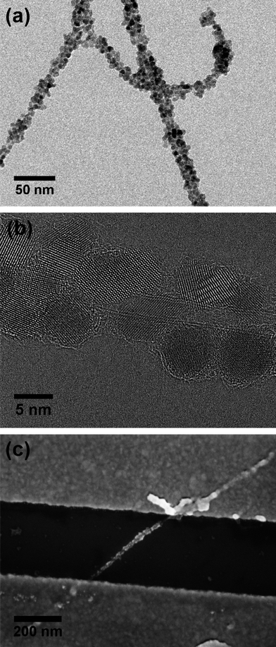 | ||
| Fig. 1 TEM images of ZnO nanoparticles obtained in the presence of DWCNTs: (a) an overview and (b) a high resolution micrograph. (c) SEM image of an individual ZnO–DWCNT contacted by gold leads forming source and drain in a FET device. | ||
Raman spectroscopy provides information about the ratio of sp3 to sp2 hybridized carbon in CNTs. Fig. 2a shows the Raman spectra of both raw DWCNTs before the decoration with ZnO nanoparticles and after the synthetic process. As can be observed, the samples synthesized at 60 °C using 2-phenyl ethanol showed similar ratio between the weak D peak (which stands for the relative amount of sp3 hybridized carbon) at 1363 cm−1 and the G peak (which represents the sp2 hybridized carbon) at 1585 cm−1.55,56 This let us assume that there is no substantial covalent functionalization of the pristine DWCNTs and upon ZnO attachment.
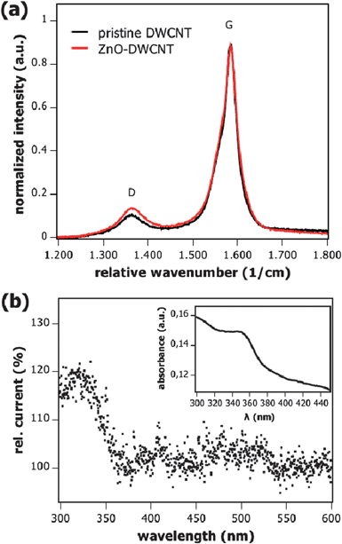 | ||
| Fig. 2 (a) Raman spectra of pristine DWCNTs and ZnO–DWCNTs composites shown in Fig. 1a and b. Both curves are scaled to the G peak. (b) Spectroscopically resolved relative current vs. wavelength of a ZnO–DWCNT FET. The current starts to change at the absorption wavelength of ZnO. The wavelength was scanned with 3 s nm−1 at a bias of VDS = +1 V and the gate voltage was held at 0 V. The measurement was performed in vacuum. The inset shows the absorption spectrum of ZnO–DWCNT composites in methanol. | ||
The optical absorption edge of the nanoparticle–nanotube composites shown in the inset of Fig. 2b lies at about 350 nm, which is somewhat smaller than the bulk value of ZnO. Taking into account that the Bohr exciton radius for ZnO lies around 2 nm,57 weak quantum confinement is observed for 5–6 nm ZnO nanoparticles. The nanoparticle size determined from the absorption spectrum58 matches well with that observed by transmission electron microscopy.
The composites of ZnO nanoparticles attached to DWCNTs were also investigated in terms of their electrical transport properties. Therefore, several FET devices were built by contacting either an individual DWCNT (blank device) or an individual ZnO–DWCNT composite with gold leads. Roughly one third of DWCNTs possess metallic properties. Thus, we chose those devices for our investigations which showed clear semiconductor behaviour. In the case of the composite material the ZnO-NPs were removed at the contact area to ensure intimate contact between DWCNT and lead metal (for details see the Methods section above). Without removal of ZnO-NPs at the contacts we measured a maximum current of 10−11 A (without illumination), which is five orders of magnitude lower than the one of DWCNT or ZnO–DWCNT with ZnO removed at the contacts under the same conditions (ESI, Fig. S3† and 3). Thus, we can exclude significant charge transport through the ZnO-NP layer.
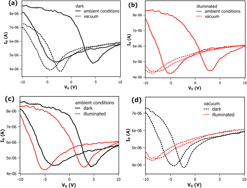 | ||
| Fig. 3 Comparison of ZnO–DWCNT-FET transfer characteristics under ambient condition (full line) and under low pressure condition (dotted line) (a) without and (b) upon white light illumination (xenon lamp, 400 W). The threshold voltage shift after change of conditions is much larger with illumination (b) than without (a). Comparison of ZnO–DWCNT-FET transfer characteristics with (red line) and without illumination (black line) (c) under ambient and (d) reduced pressure conditions shows that the threshold voltage shift upon illumination is much larger under vacuum (d) due to the lack of oxygen. All measurements were performed at a drain-source bias of VDS = +1 V. | ||
The work function of the here used DWCNTs varies in a small range around 4.9 eV.59 Since the gold leads exhibit a work function of 5.3 eV which is higher than the one of the CNTs a Schottky barrier is formed at the interface between the semiconducting nanotubes and the gold contacts. Due to the pinning in air,60 this leads to hole conduction and the device shows p-type characteristics. Both, blank devices containing only DWCNT (ESI, Fig. S3†) as well as composites (Fig. 3a) show hole conductivity without illumination. The appearing hysteresis in transfer characteristics is attributed to water adsorption and organic contamination from the lithography process according to the literature.61–64 Consequently, reduced hysteresis under low pressure condition (10−5 mbar) can be explained in terms of water desorption.61 The ZnO–DWCNT devices exhibit reduced on/off ratio compared to the blank devices, which can be understood in terms of screening of the tube by the charges of the n-type ZnO. Since the DWCNT channel is uniformly covered by ZnO nanocrystals, an additional layer is present between the Si/SiO2 substrate and the gate, which lowers the efficiency of the applied gate voltage.
Due to strong oxygen affinity ZnO adsorbs O2 readily forming O2− species at the ZnO surface. Thus, oxygen is bound to the n-type ZnO by accepting the negative charge. In addition to the negative charge transfer from nanoparticles to the oxygen molecules, the electron transfer to the CNTs in ZnO–DWCNT composites is possible, since the Fermi level in n-doped ZnO is close to its conduction band level which lies at about −4.5 eV with respect to the vacuum level65 and thus above the Fermi level of the nanotubes. In a vacuum, we expect the charge transfer from n-type ZnO to CNTs to be favoured due to the absence of oxygen. The comparison of recorded transfer characteristics of ZnO–DWCNT devices without light in Fig. 3a displays a threshold voltage shift of more than 1 V to the negative by switching from ambient to a low pressure condition, indicating the negative charge transfer from ZnO to CNTs and thus n-doping of the FET channel, as demonstrated by Heinze et al. for potassium.66 That means that by oxygen exclusion the charge transfer from ZnO to CNT becomes visible in transfer characteristics and the ZnO–DWCNT FETs are sensitive to oxygen. Comparable behaviour was not observed for pure DWCNT FETs (ESI, Fig. S4a†).
In Fig. 3b, where the transfer characteristics of illuminated devices under different conditions are displayed, an enhancement of the doping effect is indicated by a stronger threshold voltage shift. Under illumination, photo-generated electrons in ZnO are shown to follow three competitive paths in the presence of adsorbed oxygen.67 The electron can either recombine with the hole or with deep trapped holes or it can migrate to surface states. Furthermore, as described earlier, CNTs are able to accept electrons from ZnO due to favourable band alignment in the composite material. Thus, photo-generated electrons can easily pass from the nanoparticles to the closely attached nanotubes, as it could be shown for other NP–CNT systems.34,38–42,45 The hole might remain on the NP because of an unfavourable alignment of the hole state in the ZnO compared to the Fermi level of CNTs. Additionally, the n-type character of the ZnO stabilizes the positive charge on the NP.
Under ambient conditions a small threshold voltage shift of about 1 V toward negative gate voltages as well as an increase in the current at 0 V is observed upon illumination (see Fig. 3c) indicating weak photo-n-doping.66 By switching to low pressure conditions and exposing the same device to light the threshold voltage shift increases by a factor of three (see Fig. 3d). While nanotube photo-doping is competitive with the processes described above under ambient conditions (Fig. 3c), it seems to be the main path under reduced pressure as the transfer characteristics indicate in Fig. 3d.
The fact that the strong improvement of carbon nanotube n-doping upon illumination happens by switching from ambient to low pressure conditions is understood in terms of oxygen desorption from attached ZnO (Fig. 4). As mentioned above, oxygen is known to easily chemisorb on the ZnO surface. In the dark oxygen molecules can accept an electron from the n-type ZnO forming the O2− species.68 After the electron–hole pairs are generated by photon absorption, the holes migrate to the surface and discharge the O2− species, while the remaining electrons can either recombine with the remaining holes or migrate to the surface where they assist the re-adsorption of oxygen. Additionally, in the case of ZnO–CNT composite negative charge can be transferred to nanotubes. Consequently, when no oxygen is present the electron can either recombine with the hole or it can contribute to the CNT n-doping, while the hole remains stable in the particle since there are no O2− species available. The positively charged particles can be considered as an additional source of gate voltage which is very efficient since the charge is located directly at the tubes.
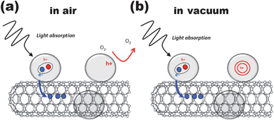 | ||
| Fig. 4 Proposed mechanism for the photo-gating effect for ZnO–DWCNTs (a) under ambient and (b) reduced pressure conditions. For simplicity, a single-walled CNT instead of a double-walled CNT is depicted. | ||
Further evidence for the photo-gating effect of ZnO on DWCNTs is found in the spectroscopically resolved photoconductivity measurements (Fig. 2b), where a corresponding change in current occurs at wavelengths shorter than 350 nm, the absorption edge of ZnO (Fig. 2b, inset). In a vacuum, the current sharply increases by up to 15% meaning that the device is reasonably sensitive to UV-light.
Conclusions
ZnO nanoparticles were grown directly on the non-functionalized carbon lattice of DWCNTs excluding long chain ligands at the NP–CNT interface by introducing the CNTs into a colloidal synthetic procedure. This methodology allows the formation of uniform and high quality NP–CNT composites with high coverage. The composites have been morphologically characterized and their gate response has been addressed and discussed in terms of a doping effect caused by closely attached n-type material and doping enhancement by illumination. Thus, ZnO–DWCNT FETs were shown to be oxygen- and light-sensitive devices demonstrating the potential of nano-composites for sensing and optoelectronic applications.Acknowledgements
The authors thank Andreas Kornowski for TEM measurements and Anton Myalitsin for the Raman characterization. Beatriz H. Juárez thanks the European Comission for ERG-04-GA-2008-239256 and the Spanish Ministry of Science and Innovation for RYC-2007-01709 and MAT2009-13488. Financial support from the Free and Hanseatic City of Hamburg in the context of the "Landesexzellenzinitiative Hamburg: Spintronics" as well as from the German Federal Ministry of Education and Research BMBF, "Sonapoly" project 08-185, is gratefully acknowledged.Notes and references
- A. B. Djurišic and Y. H. Leung, Small, 2006, 2, 944–961 CrossRef CAS.
- C. Klingshirn, ChemPhysChem, 2007, 8, 782–803 CrossRef CAS.
- U. Özgur, Y. I. Alivov, C. Liu, A. Teke, M. A. Reshchikov, S. Dogan, V. Avrutin, S.-J. Cho and H. Morkoç, J. Appl. Phys., 2005, 98, 041301 CrossRef.
- H. Saeki, H. Tabata and T. Kawai, Solid State Commun., 2001, 120, 439–443 CrossRef CAS.
- D. B. Buchholz, R. P. H. Chang, J. H. Song and J. B. Ketterson, Appl. Phys. Lett., 2005, 87, 082504 CrossRef.
- W. Prellier, A. Fouchet and B. Mercey, J. Phys.: Condens. Matter, 2003, 15, R1583–R1601 CrossRef CAS.
- M. L. Kahn, M. Monge, V. Collière, F. Senocq, A. Maisonnat and B. Chaudret, Adv. Funct. Mater., 2005, 15, 458–468 CrossRef CAS.
- Z. Hu, G. Oskam and P. C. Searson, J. Colloid Interface Sci., 2003, 263, 454–460 CrossRef CAS.
- C. Pacholski, A. Kornowski and H. Weller, Angew. Chem., Int. Ed., 2002, 41, 1188–1191 CrossRef CAS.
- M. Terrones, Annu. Rev. Mater. Res., 2003, 33, 419–501 CrossRef CAS.
- P. Avouris and J. Chen, Mater. Today, 2006, 9, 46–54 CrossRef CAS.
- H. Dai, Surf. Sci., 2002, 500, 218–241 CrossRef CAS.
- C. Klinke, J. B. Hannon, A. Afzali and P. Avouris, Nano Lett., 2006, 6, 906–910 CrossRef CAS.
- E. Artukovic, M. Kaempgen, D. S. Hecht, S. Roth and G. Grüner, Nano Lett., 2005, 5, 757–760 CrossRef CAS.
- J.-M. Bonard, K. A. Dean, B. F. Coll and C. Klinke, Phys. Rev. Lett., 2002, 89, 197602 Search PubMed.
- N. de Jonge, Y. Lamy, K. Schoots and T. H. Oosterkamp, Nature, 2002, 420, 393–395 CrossRef CAS.
- A. Kis, G. Csányi, J.-P. Salvetat, T.-N. Lee, E. Couteau, A. J. Kulik, W. Benoit, J. Brugger and L. Forró, Nat. Mater., 2004, 3, 153–157 CrossRef CAS.
- J. Cumings and A. Zettl, Science, 2000, 289, 602–604 CrossRef.
- I. Palaci, S. Fedrigo, H. Brune, C. Klinke, M. Chen and E. Riedo, Phys. Rev. Lett., 2005, 94, 175502 CrossRef CAS.
- M. Ouyang, J.-L. Huang and C. M. Lieber, Acc. Chem. Res., 2002, 35, 1018–1025 CrossRef CAS.
- M. S. Arnold, A. A. Green, J. F. Hulvat, S. I. Stupp and M. C. Hersam, Nat. Nanotechnol., 2006, 1, 60–65 CrossRef CAS.
- M. Zheng, A. Jagota, M. S. Strano, A. P. Santos, P. Barone, S. G. Chou, B. A. Diner, M. S. Dresselhaus, R. S. Mclean, G. B. Onoa, G. G. Samsonidze, E. D. Semke, M. Usrey and D. J. Walls, Science, 2003, 302, 1545–1548 CrossRef CAS.
- D. Chattopadhyay, I. Galeska and F. Papadimitrakopoulos, J. Am. Chem. Soc., 2003, 125, 3370–3375 CrossRef CAS.
- R. Krupke, F. Hennrich, H. von Löhneysen and M. M. Kappes, Science, 2003, 301, 344–347 CrossRef CAS.
- K. Keren, R. S. Berman, E. Buchstab, U. Sivan and E. Braun, Science, 2003, 302, 1380–1382 CrossRef CAS.
- P. Nikolaev, M. J. Bronikowski, R. K. Bradley, F. Rohmund, D. T. Colbert, K. A. Smith and R. E. Smalley, Chem. Phys. Lett., 1999, 313, 91–97 CrossRef CAS.
- H. Kataura, Y. Kumazawa, Y. Maniwa, Y. Ohtsuka, R. Sen, S. Suzuki and Y. Achiba, Carbon, 2000, 38, 1691–1697 CrossRef CAS.
- E. Couteau, K. Hernadi, J. W. Seo, L. Thiên-Nga, C. Mikó, R. Gaál and L. Forró, Chem. Phys. Lett., 2003, 378, 9–17 CrossRef CAS.
- C. Klinke, E. Delvigne, J. V. Barth and K. Kern, J. Phys. Chem. B, 2005, 109, 21677–21680 CrossRef CAS.
- R. V. Hull, L. Li, Y. Xing and C. C. Chusuei, Chem. Mater., 2006, 18, 1780–1788 CrossRef CAS.
- W. Huang, H. Chen and J.-M. Zuo, Small, 2006, 2, 1418–1421 Search PubMed.
- D. Wang, Z.-C. Li and L. Chen, J. Am. Chem. Soc., 2006, 128, 15078–15079 CrossRef CAS.
- S. Banerjee and S. S. Wong, Chem. Commun., 2004, 1866–1867 RSC.
- B. Juárez, C. Klinke, A. Kornowski and H. Weller, Nano Lett., 2007, 7, 3564–3568 CrossRef CAS.
- Q. Huang and L. Gao, Nanotechnology, 2004, 15, 1855–1860 CrossRef CAS.
- M. A. Correa-Duarte, J. Pérez-Juste, A. Sánchez-Iglesias, M. Giersig and L. M. Liz-Marzán, Angew. Chem., Int. Ed., 2005, 44, 4375–4378 CrossRef CAS.
- I. Robel, B. A. Bunker and P. V. Kamat, Adv. Mater., 2005, 17, 2458–2463 CrossRef CAS.
- F. Vietmeyer, B. Seger and P. Kamat, Adv. Mater., 2007, 19, 2935–2940 CrossRef CAS.
- Y. Zhu, H. Elim, Y.-L. Foo, T. Yu, Y. Liu, W. Ji, J.-Y. Lee, Z. Shen, A. Wee, J. Thong and C. Sow, Adv. Mater., 2006, 18, 587–592 CrossRef CAS.
- X. Li, Y. Jia and A. Cao, ACS Nano, 2010, 4, 506–512 CrossRef CAS.
- L. Hu, Y.-L. Zhao, K. Ryu, C. Zhou, J. Stoddart and G. Grüner, Adv. Mater., 2008, 20, 939–946 CrossRef CAS.
- A. Kongkanand, R. Martinez Dominguez and P. V. Kamat, Nano Lett., 2007, 7, 676–680 CrossRef CAS.
- C. Chen, X. Chen, B. Yi, T. Liu, W. Li, L. Xu, Z. Yang, H. Zhang and Y. Wang, Acta Mater., 2006, 54, 5401–5407 CrossRef CAS.
- G. Wildgoose, C. Banks and R. Compton, Small, 2006, 2, 182–193 CrossRef CAS.
- S. Liu, J. Ye, Y. Cao, Q. Shen, Z. Liu, L. Qi and X. Guo, Small, 2009, 5, 2371–2376 CrossRef CAS.
- M. Olek, M. Hilgendorff and M. Giersig, Colloids Surf., A, 2007, 292, 83–85 CrossRef CAS.
- L. Liu, T. Wang, J. Li, Z.-X. Guo, L. Dai, D. Zhang and D. Zhu, Chem. Phys. Lett., 2003, 367, 747–752 CrossRef CAS.
- A. B. Hungría, B. H. Juárez, C. Klinke, H. Weller and P. A. Midgley, Nano Res., 2008, 1, 89–97 Search PubMed.
- B. H. Juárez, M. Meyns, A. Chanaewa, Y. Cai, C. Klinke and H. Weller, J. Am. Chem. Soc., 2008, 130, 15282–15284 CrossRef CAS.
- B. Ritz, H. Heller, A. Myalitsin, A. Kornowski, F. J. Martin-Martinez, S. Melchor, J. A. Dobado, B. H. Juárez, H. Weller and C. Klinke, ACS Nano, 2010, 4, 2438–2444 CrossRef CAS.
- B. Chen, M. Gao, J. M. Zuo, S. Qu, B. Liu and Y. Huang, Appl. Phys. Lett., 2003, 83, 3570–3571 CrossRef CAS.
- Y. P. Gao, C. N. Sisk and L. J. Hope-Weeks, Chem. Mater., 2007, 19, 6007–6011 CrossRef CAS.
- A. H. El-Sheikh, Talanta, 2008, 75, 127–134 CrossRef CAS.
- D. Sun, M. Wong, L. Sun, Y. Li, N. Miyatake and H.-J. Sue, J. Sol-Gel Sci. Technol., 2007, 43, 237–243 CrossRef CAS.
- M. S. Dresselhaus, G. Dresselhaus, A. Jorio, A. G. S. Filho and R. Saito, Carbon, 2002, 40, 2043–2061 CrossRef CAS.
- C. Klinke, R. Kurt, J.-M. Bonard and K. Kern, J. Phys. Chem. B, 2002, 106, 11191–11195 CrossRef CAS.
- A. Wood, M. Giersig, M. Hilgendorff, A. Vilas-Campos, L. M. Liz-Marzán and P. Mulvaney, Aust. J. Chem., 2003, 56, 1051–1057 CrossRef CAS.
- R. Viswanatha, S. Sapra, B. Satpati, P. V. Satyam, B. N. Dev and D. D. Sarma, J. Mater. Chem., 2004, 14, 661–668 RSC.
- P. Liu, Q. Sun, F. Zhu, K. Liu, K. Jiang, L. Liu, Q. Li and S. Fan, Nano Lett., 2008, 8, 647–651 CrossRef CAS.
- R. Martel, T. Schmidt, H. R. Shea, T. Hertel and P. Avouris, Appl. Phys. Lett., 1998, 73, 2447–2449 CrossRef CAS.
- W. Kim, A. Javey, O. Vermesh, Q. Wang, Y. Li and H. Dai, Nano Lett., 2003, 3, 193–198 CrossRef CAS.
- H. Shimauchi, Y. Ohno, S. Kishimoto and T. Mizutani, Jpn. J. Appl. Phys., 2006, 45, 5501–5503 CrossRef CAS.
- D. Sung, S. Hong, Y.-H. Kim, N. Park, S. Kim, S. L. Maeng and K.-C. Kim, Appl. Phys. Lett., 2006, 89, 243110 CrossRef.
- M. Muoth, T. Helbling, L. Durrer, S.-W. Lee, C. Roman and C. Hierold, Nat. Nanotechnol., 2010, 5, 589–592 CrossRef CAS.
- C. G. Van de Walle and J. Neugebauer, Nature, 2003, 423, 626–628 CrossRef CAS.
- S. Heinze, J. Tersoff, R. Martel, V. Derycke, J. Appenzeller and P. Avouris, Phys. Rev. Lett., 2002, 89, 106801 CrossRef CAS.
- A. van Dijken, E. A. Meulenkamp, D. Vanmaekelbergh and A. Meijerink, J. Phys. Chem. B, 2000, 104, 1715–1723 CrossRef CAS.
- H. Kind, H. Yan, B. Messer, M. Law and P. Yang, Adv. Mater., 2002, 14, 158–160 CrossRef CAS.
Footnote |
| † Electronic supplementary information (ESI) available: Fig. S1, TEM image of the composite system right after nucleation of the nanoparticles around the tubes. Fig. S2, XRD diffractogram of the composite. Fig. S3 and S4, charge transfer characteristics of DWCNT FET without ZnO nanoparticles. See DOI: 10.1039/c1nr11284h |
| This journal is © The Royal Society of Chemistry 2012 |