Diamond nanowires for highly sensitive matrix-free mass spectrometry analysis of small molecules
Yannick
Coffinier
*ab,
Sabine
Szunerits
ab,
Hervé
Drobecq
c,
Oleg
Melnyk
c and
Rabah
Boukherroub
ab
aInstitut de Recherche Interdisciplinaire (IRI-CNRS-3078), Université Lille1, Parc scientifique de la haute borne, 50 Avenue de Halley, 59658, Villeneuve d'Ascq, France
bInstitut d'électronique, de microélectronique et de nanotechnologies (IEMN-CNRS-8520), Avenue Poincaré, 59650, Villeneuve d'Ascq, France. E-mail: yannick.coffinier@iri.univ-lille1.fr; Fax: +33 3 20 19 78 84; Tel: +33 3 20 19 79 87
cInstitut de Biologie de Lille, (IBL-CNRS-8160), Rue du professeur Calmette, Lille, France
First published on 14th November 2011
Abstract
This paper reports on the use of boron-doped diamond nanowires (BDD NWs) as an inorganic substrate for matrix-free laser desorption/ionization mass spectrometry (LDI-MS) analysis of small molecules. The diamond nanowires are prepared by reactive ion etching (RIE) with oxygen plasma of highly boron-doped (the boron level is 1019 B cm−3) or undoped nanocrystalline diamond substrates. The resulting diamond nanowires are coated with a thin silicon oxide layer that confers a superhydrophilic character to the surface. To minimize droplet spreading, the nanowires were chemically functionalized with octadecyltrichlorosilane (OTS) and then UV/ozone treated to reach a final water contact angle of 120°. The sub-bandgap absorption under UV laser irradiation and the heat confinement inside the nanowires allowed desorption/ionization, most likely via a thermal mechanism, and mass spectrometry analysis of small molecules. A detection limit of 200 zeptomole for verapamil was demonstrated.
Introduction
Matrix-assisted laser desorption/ionization mass spectrometry (MALDI-MS) is a soft ionization technique, developed in the late 1980s, for mass analysis of analytes. MALDI allows the analysis of a wide variety of compounds, including polymers, peptides, and proteins.1 However, due to a competitive desorption of parasitic ions from the matrix, it is difficult to detect low molecular weight compounds (<700 Da) even though small biomolecules are known to play an important role in regulating cellular functions, for biomarker discovery and disease diagnosis.2–5 To enable desorption/ionization of small molecules, techniques based on surface-assisted laser desorption/ionization (SALDI) were proposed in the literature.6,7 The techniques rely on the use of inorganic (nano- or micro-sized metal or carbon particles) substrates instead of organic matrices, yielding low background signals and thus high ionization efficiency of small molecules (below 500 Da).6,8 Direct analysis of compounds is also possible from intact thin-layer chromatography (TLC) plates by SALDI/MS.9 In 1999, matrix-free desorption/ionization on porous silicon (DIOS) was introduced, as alternative to the MALDI technique, for the analysis of low-molecular mass compounds.10,11 The porous silicon substrate is easily obtained by electrochemical anodization of crystalline silicon in HF-based solutions. Using the same mass spectrometer, as for MALDI (i.e. N2 laser λ = 327 nm and time of flight (ToF) analyser), an optimal performance for molecules less than 3000 Da was obtained.12,13 Since then, many other matrix-free methods have been developed for laser desorption/ionization (LDI) analysis.7 Various micro- or nanostructured inorganic substrates have been successfully used for matrix-free LDI, also called SALDI-MS, such as germanium nanodots,14gold and silver nanoparticles,15,16platinum nanoflowers,17boron nitride, zinc oxide, silicon nanowires18–21 and porous alumina.22Carbon-based interfaces such as carbon-like graphite, carbon nanotubes, fullerenes, or amorphous carbon have also been employed as SALDI substrates for the detection of small macromolecules such as synthetic polymers and biomolecules.23–25 Still some improvements have to be made in the case of fullerenes and fullerene-derivatives as they show poor sensitivity.26–28 In contrast to fullerenes, carbon nanotubes exhibit a very high sensitivity, but they are hardly soluble in aqueous solutions, which limit their use in bioanalytical applications. More recently, diamond-like carbon (DLC), an amorphous carbon with mixed levels of sp3 and sp2 hybridized carbons, has been successfully used for matrix-free LDI-MS, particularly for the analysis of small metabolites such as carbohydrates, lipids, and low-molecular-weight peptides.29 The physical characteristics of these nanostructured substrates such as thermal, electrical and chemical properties play a pivotal role in the LDI processes.29Here, we demonstrate, for the first time, the use of diamond nanowires as a matrix-free LDI substrate for the D/I of peptides and small molecules, and their analysis by mass spectrometry with a very high sensitivity. Fabrication of the diamond nanowire substrate was achieved via a maskless reactive ion etching (RIE) of highly boron-doped or undoped nanodiamond film using oxygen plasma.30–32 This straightforward method displays several advantages as it does not require any complicated processing steps such as mask deposition or template removal.
Experimental
Diamond nanowire preparation
2 μm-thick nanocrystalline boron-doped (NcBDD) (boron level: 3 × 10¹⁹ B cm−3) or undoped (NcUDD) diamond films, deposited on silicon substrates, were provided by Rhobest (Innsbruck, Austria). The size of the specimen was typically 1 × 1 cm2 and used as received. Reactive ion etching (RIE) was performed using oxygen plasma with an oxygen pressure and a flow rate of 150 mTorr and 20 sccm, respectively, and a plasma power of 300 W during 40 min (OXFORD Plasmalab 80plus, UK).30,31 Prior to etching, the plasma chamber is cleaned by rinsing with isopropyl alcohol followed by an oxygen plasma under the same etching conditions described above for better reproducibility. Then, the NCD surface is introduced and processed.Diamond nanowire chemical modification
Freshly prepared nanowires were UV/ozone-treated (UVO Cleaner, Jelight Company, Inc., USA, 4 mW cm−2 at 220 nm) for 20 min to remove organic contaminants on the surface and to generate surface hydroxyl groups. The resulting interface was dipped in a 10−3 M solution of octadecyltrichlorosilane (OTS, ABCR GmbH) in hexane for 6 h in a dry nitrogen purged glove box at room temperature. Then, the interface was thoroughly rinsed with hexane, dichloromethane and ethanol and finally dried under a gentle steam of nitrogen.31BDD nanowire wettability control
The OTS-terminated BDD nanowire surfaces display a superhydrophobic character with a water contact angle higher than 150°. A water droplet on the surface has a tendency to roll off. To facilitate analyte deposition, the contact angle was decreased to 120° via exposure of the OTS layer to UV ozone irradiation for 5 min.Scanning electron microscopy (SEM)
SEM images were recorded using an electron microscope ULTRA 55 (Carl Zeiss) equipped with a thermal field emission emitter and a high-efficiency In-lens SE detector.Contact angle measurements
Water contact angles were measured using deionized water. We used a remote-computer controlled goniometer system DIGIDROP (GBX, France) for measuring the contact angles. The accuracy is ±2°. All measurements were made in ambient atmosphere at room temperature.Reflectance measurements
The reflectance measurements were performed using a UV-vis spectrophotometer (Perkin-Elmer Lambda UV/Vis 950 spectrophotometer) equipped with an integrating sphere. The scans were measured for wavelength ranging from 200 to 800 nm at an incident light angle of 45° and at different locations on each scanned surface.Sample preparation
The peptide sample mix composed of [Des-Arg1]-bradykinin (MW = 904.5 Da), angiotensin I (MW = 1295.7 Da), [Glu1]-fibrinopeptide B (MW = 1570 Da) and neurotensin (MW = 1672.9 Da) was obtained from a sequazyme peptide mass standard kit of Applied Biosystems (Part number P2-3143-00). The peptide solutions were then diluted in a 1 mM ammonium citrate aqueous solution to a concentration of 50 fmol μL−1 (10 fmol μL−1 for neurotensin). Verapamil, histidine, betaine, and cortisone were purchased from Aldrich and diluted in 1 mM ammonium citrate aqueous solution at 1 pmol μL−1.LDI-MS analysis
LDI-MS analyses were performed using a Voyager-DE-STR time-of-flight (ToF) mass spectrometer (Applied Biosystems, USA) with delayed extraction, operating with a pulsed N2 laser at 337 nm (3 ns pulse). Diamond nanowire interfaces were attached to the usual MALDI target using conductive double-side carbon tape. Positive ion mass spectra were acquired with a reflector mode of operation, an accelerating potential of 20 KV, and a grid voltage at 73%. The extraction delay time was 200 ns. Each spectrum is the result of ∼50 averaged laser pulses.Results and discussion
Fabrication of diamond nanowires
The diamond nanowires investigated in this work were prepared using RIE of highly boron doped or undoped nanocrystalline diamond films using oxygen plasma. Since the etching occurs in the absence of a physical mask, it was recently established that the boron dopant atoms in the diamond could act as a mask during oxygen plasma etching of heavily doped (2.1 × 10²¹ B cm−3) BDD films using RIE.32 The study showed that the formation sites were limited to areas along the grain boundaries for a BDD substrate with a boron doping level of 4.3 × 10¹⁹ B cm−3. By increasing the doping level, boron distribution expands from the grain boundaries to the facet areas. For a boron doping level of 2.1 × 10²¹ B cm−3, a heterogeneous and high density of diamond nanowires (BDD NWs) was obtained homogeneously on the surface.33 However, in our study, RIE processing of undoped diamond substrate under the same experimental conditions, as already described above, led to the formation of undoped diamond nanowires (UDD NWs). This suggests that boron atoms are not essentially involved in the nanowire formation mechanism.Fig. 1A displays a SEM image of the starting boron-doped nanocrystalline diamond substrate. It shows a relatively smooth and homogeneous surface comprising grains of 10–15 nm in size.34,35RIE etching using oxygen plasma of the diamond substrate led to the formation of diamond nanowires. Fig. 1B and C exhibit SEM representative images of doped and undoped nanocrystalline diamond substrates etched for 40 min, respectively. They consist of nanowires of 660 nm in length with a tip and a base diameter of 10 and 30 nm, respectively for both BDD and UDD nanowires. However, the UDD substrate exhibits a lower density of nanowires.
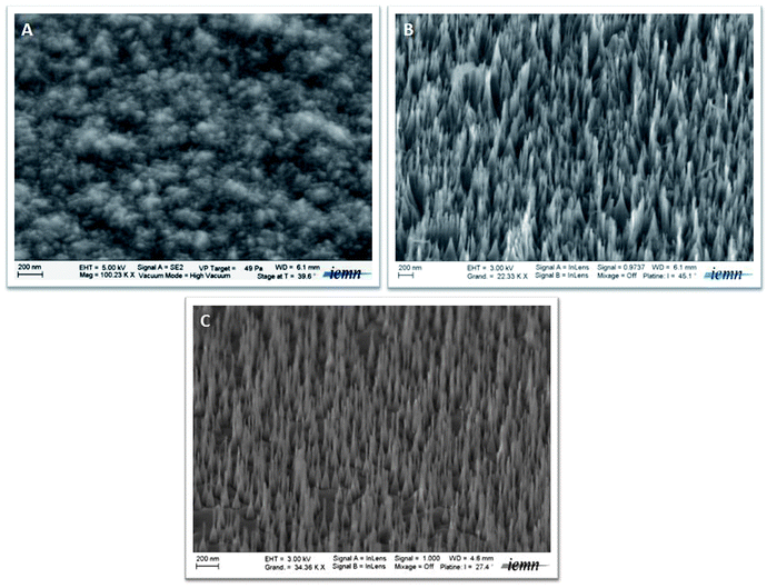 | ||
| Fig. 1 SEM images of the starting nanocrystalline boron-doped diamond substrate (A), and nanowires obtained from boron-doped (B) and undoped (C) nanocrystalline diamond interfaces. | ||
High resolution transmission electron microscopy (HRTEM) indicated that the nanowires present a crystalline core with a cubic structure and a carbon-diamond lattice covered by a silicon oxide shell (5–10 nm), which can easily be dissolved by a simple immersion in a diluted HF aqueous solution.30
The presence of silicon oxide (SiOx) deposits originates most likely from contamination in the plasma chamber due essentially to sputtering of the quartz holder or Si atoms from the edges of the Si substrate on which the NCD was deposited. However, we cannot exclude the contribution of these inorganic species from acting as a mask during the etching process. Indeed, silicon, metal (Au, Al, Mo, …) and their oxides are known to be etching masks for diamond nanostructure fabrication.36–38 Nevertheless, the present case does not appear to involve this mechanism. Indeed, the SiOx overlayer was found located all around the nanowires and not only on the top of the wires as observed for diamond nanostructures formed by using metallic masking.33,39,40
The antireflective properties of the diamond nanostructured surfaces have been evaluated. Fig. 2 exhibits the reflectance spectra of bare silicon, UDD and BDD nanowire substrates. The bare silicon showed reflectivity values between 55 and 30% in the wavelength range of 200–500 nm and values between 30 and 25% for wavelengths ranging from 500 to 800 nm. Interestingly, both UDD and BDD nanowires show better antireflective properties in comparison to bare silicon, BDD and UDD films. At 337 nm wavelength of the laser used for LDI-MS analysis, the reflectance of the nanostructured surfaces are 1.2 and 0.7% for UDD and BDD nanowires, respectively whereas flat BDD and UDD nanocrystalline films present reflectivity values of 9.8 and 10%, respectively (data not shown). Then, the reflectance of BDD nanowires increases linearly to 6% at 800 nm. However, the reflectance measured for UDD nanowires displays some optical fringes (light scattering) probably due to a heterogeneous distribution of nanowires on the surface. Despite the fact that the BDD nanowire surfaces have only shown slightly higher antireflective properties in comparison to UDD nanowires, they should have higher photon absorption thanks to a homogeneous density of black layer of wires.41
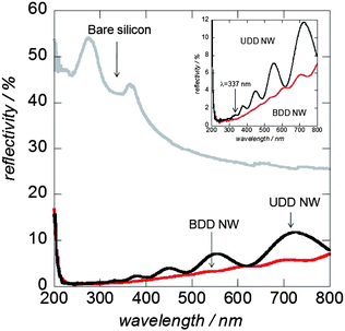 | ||
| Fig. 2 Reflectivity spectra of bare silicon, BDD and UDD nanowires. | ||
The presence of a silicon oxide coating layer confers a superhydrophilic character to the diamond nanowire surface. This wetting state is not optimal to perform LDI-MS experiments. Indeed, a droplet of analytes deposited on the substrate wets completely the surface, limiting the sensitivity. The presence of silanol groups on the surface allows chemical functionalization of the nanowire substrate through silanization with octadecyltrichlorosilane (OTS). The resulting OTS-terminated surface displays a superhydrophobic character with a contact angle higher than 150°. Due to the rolling ball effect, i.e. a sample droplet deposited on the nanowire surface rolls off very easily, the CA was reduced to 120° through UV/ozone irradiation for 5 min. This CA facilitates the droplet deposition and thus concentrates the analytes on a very small and uniform spot, allowing an optimal MS signal.
LDI-MS analysis of small molecules
For LDI-MS experiments: a 1 μL droplet containing 50 fmol μL−1 of a peptide mixture, Des-Arg1-bradykinin (904 Da), angiotensin I (1296 Da), fibropeptide (1571 Da) and neurotensin (1672 Da, 10 fmol μL−1), was deposited on the diamond nanowire surface, dried and then exposed to a pulsed nitrogen laser (λ = 337 nm, 3.68 eV). The diamond nanowires act as an energy absorbing material. It should be noticed that the SiOx overlayer was kept during the LDI-MS experiments to favor heat confinement inside the diamond nanowires.In Fig. 3A is shown the mass spectrum of the peptide mixture obtained on BDD NWs interface. As one can see, all peptides have been detected with relatively high signal intensity. As a control, the same experiment was performed on a planar nanocrystalline BDD, i.e. the same interface without any RIE step process etching. The absence of peaks in the MS spectrum (Fig. 3B) clearly indicates that the presence of nanostructures on the BDD substrate is mandatory for achieving D/I of biomolecules.
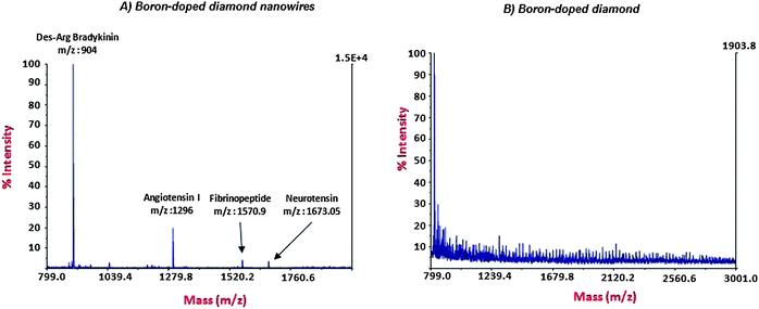 | ||
| Fig. 3 MS spectra obtained for a peptide mixture (50 fmol μL−1) on BDD NWs (A) and NcBDD starting material (B) substrates. | ||
Table 1 displays the signal to noise (S/N) ratio values for the detected peptides by LDI-MS on BDD and UDD NWs. The S/N ratios obtained on BDD nanowires are 1078, 431, 55 and 59.3 for [Des-Arg1]-bradykinin, angiotensin I, [Glu1]-fibrinopeptide B, and neurotensin, respectively, whereas those obtained on UDD nanowires are 115, 44, 8.3 and 4.3. We can notice that the S/N ratio values obtained using the UDD NWs are very low in comparison with those of BDD NWs, suggesting that to reach an efficient D/I on diamond, the surface should be nanostructured with a dense layer of wires and display antireflective properties.
| Analytes | Concentrations/μL | Main peak (m/z) | Signal/noise BDD NW | Signal/noise UDD NW | Fragments/adducts (m/z) |
|---|---|---|---|---|---|
| a 2 pmol, 200 amol and 200 zmol, respectively. | |||||
| Des-Arg1 bradykinin | 50 fmol | 904 | 1078 | 115 | — |
| Angiotensin I | 50 fmol | 1296 | 431 | 44 | — |
| [Glu1]-fibrinopeptide B | 50 fmol | 1570.9 | 55 | 8.3 | — |
| Neurotensin | 10 fmol | 1673.05 | 59.3 | 4.3 | — |
| Verapamil | 2 pmol, 200 amol and 200 zmol | 455 | 1187, 457 and 41a | — | 303 |
| Betaine | 1 pmol | 118.1 | 318 | — | — |
| Histidine | 1 pmol | 156 | 453 | — | −178 [M + Na]+ |
| Cortisone | 1 pmol | 361 | 20 | — | — |
We also investigated a variety of small molecules with mass ranging from 100 to 460 Da (Fig. 4). Verapamil, which is used in the treatment of hypertension, angina pectoris, cardiac arrhythmia, and most recently, cluster headaches, has been tested at different concentrations (2 pmol, 200 amol and 200 zmol μL−1). Verapamil, molecular ion [M + H]+ at m/z 455 (base peak) was detected for all the tested concentrations with S/N ratios of 1187, 457 and 41 for 2 pmol, 200 amol and 200 zmol μL−1, respectively (Table 1).
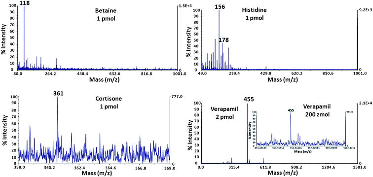 | ||
| Fig. 4 MS spectra of betaine, histidine, cortisone and verapamil (m/z 118, 156, 361 and 455, respectively). The inset shows the spectrum of verapamil at 200 zmol. | ||
A known verapamil fragment was also detected at m/z 303 at 2 pmol μL−1. The functionalized BDD NWs provided a detection limit of 200 zmol μL−1 for verapamil (see inset in Fig. 4). This demonstrates the high sensitivity of the diamond nanowire substrate for LDI-MS analysis of small molecules and its high potential as a D/I inorganic matrix. Other small molecules at 1 pmol μL−1 were also detected as [M + H]+, including betaine (m/z 118), histidine (m/z 156) and its sodium adduct [M + Na]+ at m/z 178, and cortisone (m/z 361) (Fig. 4). The corresponding S/N values are summarized in Table 1.
Moreover, it has to be noted, that no parasitic adducts or ions from the OTS layer have been observed in all MS spectra, showing that the hydrophobic layer is stable under UV irradiation. Indeed, in Fig. 4 we can easily see a clean spectrum corresponding to verapamil at 2 pmol. Moreover, in a control experiment, direct laser irradiation of the OTS modified BDD nanowires without analyte deposition was performed. In that case, no MS signal has been detected. Additionally, no apparent morphological changes of the surface upon laser irradiation have been observed by SEM (data not shown).
The analysis of small molecules has been successfully performed proving that diamond nanowires can be used as a versatile platform for mass spectrometry analysis of different small compounds. Despite the fact that the detection limit of diamond nanowires was not evaluated for all tested small molecules except for verapamil, good sensitivities were obtained (see Table 1) and are as good as or better than reported values in the literature. For example, Jemere et al. have reported a detection limit on nanostructured silicon (Si) thin films in the sub-fmol level (87 amol for Des-Arg9-bradykinin, 243 amol for the ACTH fragment, 25 amol for angiotensin-I and 1.0 fmol for verapamil).42 Other reported values for DIOS-MS of small peptides using electrochemically etched porous silicon (800 ymol for Des-Arg9-bradykinin and and 4 pmol for Leu-Enkephalin-Arg),43,44 porous SiO2 (50 fmol for the tripeptide LGG),45 column/void-network-deposited silicon films (50 fmol for [Des-Pro3-Ala 2,6]-bradykinin),46 porous alumina (4.3 pmol for bradykinin),41 SiNWs (500 amol for Des-Arg9-bradykinin and 5 fmol for verapamil),19,47Pt nanoflowers (700 amol for angiotensin-I)48 and silicon nanoparticles (33 fmol for verapamil),49 and activated carbon (100 nmol for 10 steroids).50
Discussion
In this study, we present a new surface-assisted laser desorption/ionization (SALDI) substrate based on nanostructured diamond substrates for highly sensitive mass spectrometry analysis of small molecules.The elucidation of the SALDI ionization mechanism is possibly the most controversial and elusive area of the SALDI technique. The SALDI mechanism can be subdivided into absorption, retention, radiation coupling and transfer, desorption and ionization reactions. To perform SALDI-MS analysis, the interfaces should be able to absorb photons from the pulsed laser. Then, thanks to a thermal mechanism relaxation via non-radiative recombination (phonons) of electrons and holes, desorption/ionization of analytes can occur.
Optical sub-bandgap absorption
Although diamond NWs may have exceptional mechanical,51 optical52,53 and electronic properties,54 there is still a great deal of work that has to be done. Indeed, experimental characterization of the electronic and optoelectronic, mechanical and optical properties of the various nanowhiskers, nanowires and nanorods have not yet been reported, nor has the structural stability of these structures been examined under irradiation or annealing.However, here, we attempted to discuss how the diamond nanowire surface, which has an indirect and large bandgap Eg of 5.5 eV, is able to perform sub-bandgap absorption of photons followed by D/I of analytes and their subsequent MS analysis. Indeed, in this study, the laser energy used for the LDI-MS analysis is ∼3.68 eV (λ = 337 nm), which is below the bandgap of diamond and thus, not sufficient enough to make photons to be absorbed by the diamond surface.
The nature of the interaction between a material and a pulsed laser is largely dependent on the energy bandgap of the material and the energy of the incident photons. If the photon energy is greater than the bandgap, then single photon absorption dominates and an electron in the valence band is promoted to the conduction band leaving a hole. In diamond nanowires, an indirect bandgap, the electron–hole recombination is a non-radiative process involving phonons for the energy dissipation (heat).
In this study, we have observed that for the realization of LDI on such diamond surface, nanostructuration of the NCD film is required (formation of diamond nanowires). The investigated diamond nanowires, undoped (UDD) or boron-doped (BDD), display antireflective properties permitting photons absorption at λ = 337 nm. However, the BDD nanowires have shown the best results in terms of analytes detection and signal quality for standard peptides, i. e. signal to noise ratio and signal intensity probably due to more efficient photons absorption (black layer).
It is known that a boron-doped diamond film has an optically active energy level within the bandgap at 0.38 eV (boron activation energy) above the valence band.55 However, this additional energy band from boron impurities is not sufficient to explain the sub-bandgap absorption. Indeed, the band-gap is still higher than the photon energy of the UV laser. Nevertheless, it is known that at a low doping level, this band is isolated, whereas at a high doping level, the impurity band may overlap with the top states of the valence band because of their very close energies that could help the sub-bandgap absorption.56 Moreover, many types of crystal defects, including the standard intrinsic ones, like vacancies, interstitials and dislocations, surface defects, and grain boundaries, have been reported for diamonds.57 These defects with their associated properties can cause electronic levels within the band gap of diamond and thus facilitate the sub-bandgap absorption of photons with energy below 5.45 eV. The role of defects, impurities in the structure, stability of 1-D diamond nanostructures, and optical and electronic properties is not yet well understood. However, some preliminary theoretical studies have been undertaken using ab initio methods by Barnard and co-workers to examine the effect of various dopants on the structural stability of ultra-fine cylindrical diamond nanowires. These studies examined the effects of various types of dopants (boron, nitrogen, oxygen, aluminium, phosphorus and sulfur) included equidistant along the axis of the nanowires.58,59 It has been shown that the diameter and surface defects can modify the band-gap of diamond nanowires. In that case, the photon energy of the laser could be enough to be absorbed by the diamond nanowires. However, this was demonstrated for diamond nanowires with a size <4 nm, and to the best of our knowledge, no theoretical or experimental studies have been undertaken on larger diamond nanowires.60
So, we can hypothesize that the combination of anti-reflective properties with additional energy levels within the bandgap in BDD nanowires has led to more efficient sub-bandgap absorption of photons in comparison with UDD nanowires allowing better LDI-MS analysis of small molecules.
Thermal confinement
It is well known that diamond films have high thermal conductivity and diffusivity due, in particular, to the efficiency of phonon's travel through the lattice (indirect band gap) leading to heat dissipation.61 However, it was demonstrated that, upon a laser irradiation of silicon nanowires (SiNWs), in a D/I experiment, the heat dissipation is arrested because of the decreased conductivity and thermal confinement in the nanowires. Compared to macroscopic targets, this leads to an elevated surface temperature on these structures, or conversely, for SiNWs, lower laser fluence is sufficient to reach the same surface temperature as a macroscopic target leading to efficient D/I.48,62 Guo et al. have also shown that the diamond nanowire geometry can greatly influence their thermal conductivity.63 Indeed, the latter increases with increasing the NWs' length and cross-sectional area. In that case, the phonon–phonon interactions and the boundary scattering are reduced, resulting in thermal conductivity increase. They have also demonstrated that the thermal conductivity in diamond nanowires is temperature dependent: by increasing the temperature, the thermal conductivity decreases. In this study, we used a pulsed laser for MS analysis causing a rapid increase of the local temperature inside the wires. Furthermore, the small size of the diamond nanowires contributes to their low thermal conductivity. Moreover, the presence of a silicon dioxide layer (5–10 nm), acting as a thermal insulator,64 also contributes to heat confinement inside the wires by lowering the thermal conductivity, leading to a significant increase of the D/I efficiency. It has to be noted that by removing the oxide layer by simply dipping the interface in HF aqueous solution led to a weak MS signal (data not shown).Thus, we can hypothesize that on BDD NW interfaces, the ionization of analytes occurs mainly via a thermal mechanism. Briefly, the boron-doped diamond nanowires absorb photons incoming from the laser. The energy is then dissipated via non-radiative recombination (phonons), leading to heat confinement within the nanowires. This heat confinement is mainly due to the diamond nanowire size and the presence of a SiOx overlayer. Since the heat dissipation is arrested, thermal ionization of analytes can take place.
Conclusion
Boron-doped diamond nanowire substrate was successfully used as an energy absorbing material under UV laser irradiation, allowing D/I of small molecules and their mass spectrometry analysis. The sub-bandgap absorption and heat confinement inside the wires lead to thermal ionization of analytes. The sensitivity is at about the fmol level for the tested peptides. A set of small molecules have also been assessed with m/z ranging from 100 to 460 including an amino acid and a corticosteroid. A detection limit of 200 zmol μL−1 for verapamil was attained using these substrates. The requirements for the realization of the LDI process using diamond interface are: the diamond should be nanostructured (dense black layer of nanowires), small sized, and highly doped and should provide a thermal confinement inside the wires through SiOx overlayer coating.Future work will focus on D/I of other relevant molecules such as more complex carbohydrates and lipids, and small proteins. Moreover, an investigation of the influence of the doping level of boron on the D/I efficiency will help us gain a better understanding of the mechanism due to accurate optical characterization.
Acknowledgements
The European Community's Seventh Frame-work Programme (FP7/20072013) under grant agreement no. 227243, the Centre National de la Recherche Scientifique (CNRS) and the Nord-Pas-de Calais region are gratefully acknowledged for financial support.References
- M. Karas and F. Hillenkamp, Anal. Chem., 1988, 60, 2299–2301 CrossRef CAS.
- A. Rivkin, T.-C. Chou and S. J. Danishefsky, Angew. Chem., Int. Ed., 2005, 44, 2838–2850 CrossRef CAS.
- S. Rochfort, J. Nat. Prod., 2005, 68, 1813–1820 CrossRef CAS.
- C. A. Smith, G. O. Maille, E. J. Want, C. Qin, S. A. Trauger, T. R. Brandon, D. E. Custodio, R. Abagyan and G. Siuzdak, Ther. Drug Monit., 2005, 27, 747–751 CrossRef CAS.
- E. J. Want, G. O'Maille, C. A. Smith, T. R. Brandon, W. Uritboonthai, C. Qin, S. A. Trauger and G. Siuzdak, Anal. Chem., 2006, 78, 743–752 CrossRef CAS.
- K. Tanaka, H. Waki, Y. Ido, S. Akita, Y. Yoshida and T. Yoshida, Rapid Commun. Mass Spectrom., 1988, 2, 151–153 CAS.
- D. S. Peterson, Mass Spectrom. Rev., 2007, 26, 19–34 CrossRef CAS.
- P. Kraft, S. Alimpiev, E. Dratz and J. Sunner, J. Am. Soc. Mass Spectrom., 1998, 9, 912–924 CrossRef CAS.
- Y. C. Chen, J. Shiea and J. Sunner, J. Chromatogr., A, 1998, 826, 77–86 CrossRef CAS.
- J. Wei, J. M. Buriak and G. Siuzdak, Nature, 1999, 399, 243–246 CrossRef CAS.
- N. Budimir, J. C. Blais, F. Fournier and J. C. Tabet, Rapid Commun. Mass Spectrom., 2006, 20, 680–684 Search PubMed.
- J. J. Thomas, Z. Shen, J. E. Crowell, M. G. Finn and G. Siuzdak, Proc. Natl. Acad. Sci. U. S. A., 2001, 98, 4932–4937 CrossRef CAS.
- W. G. Lewis, Z. Shen, M. G. Finn and G. Siuzdak, Int. J. Mass Spectrom., 2003, 226, 107–116 Search PubMed.
- T. Seino, H. Sato, A. Yamamoto, A. Nemoto, M. Torimura and H. Tao, Anal. Chem., 2007, 79, 4827–4832 Search PubMed.
- E. T. Castellana and D. H. Russell, Nano Lett., 2007, 7, 3023–3025 CrossRef.
- L. Hua, J. Chen, L. Ge and S. N. Tan, J. Nanopart. Res., 2007, 9, 1133–1138 CrossRef CAS.
- H. Kawasaki, T. Yonezawa, T. Watanabe and R. Arakawa, J. Phys. Chem. C, 2007, 111, 16278–16283 CrossRef CAS.
- M.-J. Kang, J.-C. Pyun, J.-C. Lee, Y.-J. Choi, J.-H. Park, J.-G. Park, J.-G. Lee and H.-J. Choi, Rapid Commun. Mass Spectrom., 2005, 19, 3166–3170 CrossRef CAS.
- G. Piret, H. Drobecq, Y. Coffinier, O. Melnyk and R. Boukherroub, Langmuir, 2010, 26, 1354–1361 CrossRef CAS.
- G. Piret, R. Desmet, E. Diesis, H. Drobecq, J. Seegrs, C. Rouanet, A.-S. Debrie, R. Boukherroub, C. Locht and O. Melnyk, J. Proteome Res., 2010, 9, 6467–6478 CrossRef CAS.
- F. Lapierre, G. Piret, H. Drobecq, O. Melnyk, Y. Coffinier, V. Thomy and R. Boukherroub, Lab Chip, 2011, 11, 1620–1628 RSC.
- R. Nayak and D. R. Knapp, Anal. Chem., 2007, 79, 4950–4956 Search PubMed.
- M. J. Dale, R. Knochenmuss and R. Zenobi, Anal. Chem., 1996, 68, 3321–3329 CrossRef CAS.
- S. Ren, L. Zhang, Z. Cheng and Y. Guo, J. Am. Soc. Mass Spectrom., 2005, 16, 333–339 CrossRef CAS.
- F. G. Hopwood, L. Michalak, D. S. Alderdice, K. J. Fisher and G. D. Willett, Rapid Commun. Mass Spectrom., 1994, 8, 881–885 CAS.
- A. K. Kalkan and S. J. Fonash, MRS Online Proc. LIbr., 2003, 788, 595–600 Search PubMed.
- J. Shiea, J. P. Huang, C. F. Teng, J. Jeng, L. Y. Wang and L. Y. Chiang, Anal. Chem., 2003, 75, 3587–3595 CrossRef CAS.
- Z. Szabo, R. M. Vallant, A. Takatsy, R. Bakry, M. Najam-ul-Haq, M. Rainer, C. W. Hucka and G. K. Bonn, J. Mass Spectrom., 2010, 45, 542–552 Search PubMed.
- M. Najam-ul-Haq, M. W. Rainer, C. Huck, P. Hausberger, H. Kraushaar and G. K. Bonn, Anal. Chem., 2008, 80, 7467–7472 CrossRef CAS.
- S. Szunerits, Y. Coffinier, E. Galopin, J. Brenner and R. Boukherroub, Electrochem. Commun., 2010, 12, 438–441 CrossRef CAS.
- Y. Coffinier, E. Galopin, S. Szunerits and R. Boukherroub, J. Mater. Chem., 2010, 20, 10671–10675 RSC.
- M. Wei, C. Terashima, M. Lv, A. Fujishima and Z.-Z. Gu, Chem. Commun., 2009, 3624–3626 RSC.
- C. Terashima, K. Arihara, S. Okazaki, T. Shichi, D. A. Tryk, T. Shirafuji, N. Saito, O. Takai and A. Fujishima, ACS Appl. Mater. Interfaces, 2011, 3, 177–182 Search PubMed.
- F. Klauser, S. Ghodbane, R. Boukherroub, S. Szunerits, D. Steinmüller-Nethl, E. Bertel and N. Memmel, Diamond Relat. Mater., 2010, 19, 474–478 Search PubMed.
- S. Ghodbane, T. Haensel, Y. Coffinier, S. Szunerits, D. Steinmüller-Nethl, R. Boukherroub, S. Imad-Uddin Ahmed and J. A. Schaefer, Langmuir, 2010, 26, 18798–18805 Search PubMed.
- Y. S. Zou, Y. Yang, W. J. Zhang, Y. M. Chong, B. He, I. Bello and S. T. Lee, Appl. Phys. Lett., 2008, 92, 1–3 CrossRef.
- E. S. Baik, Y. J. Baik and D. Jeon, J. Mater. Res., 2000, 15, 923–926 CAS.
- C. Y. Li and A. Hatta, Diamond Relat. Mater., 2005, 14, 1780–1783 Search PubMed.
- M. D. Stoikou, P. John and J. I. B. Wilson, Diamond Relat. Mater., 2008, 17, 1164–1168 Search PubMed.
- C. Y. Li and A. Hatta, Thin Solid Films, 2007, 515, 4172–4176 Search PubMed.
- R. Nayak and D. R. Knapp, Anal. Chem., 2007, 79, 4950–4956 Search PubMed.
- A. B. Jemere, L. W. Bezuidenhout, M. J. Brett and D. J. Harrison, Rapid Commun. Mass Spectrom., 2010, 24, 2305–2311 CrossRef CAS.
- S. Tumikoski, K. Huikko, K. Grigoras, P. Ostman, R. Kostiainen, M. Baumann, J. Abian, T. Kotiaho and S. Franssila, Lab Chip, 2002, 2, 247–253 RSC.
- S. A. Trauger, E. P. Go, Z. Shen, J. V. Apon, B. J. Compton, E. S. P. Bouvier, M. G. Finn and G. Siuzdak, Anal. Chem., 2004, 76, 4484–4489 CrossRef.
- A. G. Drazazga, S. Bargiel, R. Walczak, J. A. Dziuban, A. Kraj, T. Dylag and J. Silberring, Sens. Actuators, B, 2004, 103, 206–212 CrossRef.
- N. H. Finkel, B. G. Prevo, O. D. Velev and L. He, Anal. Chem., 2005, 77, 1088–1095 CrossRef CAS.
- E. P. Go, J. V. Apon, G. Luo, A. Saghatelian, R. H. Daniels, V. Sahi, R. Dubrow, B. F. Cravatt, A. Vertes and G. Siuzdak, Anal. Chem., 2005, 77, 1641–1646 CrossRef CAS.
- L. Buckberry and S. C. Bayliss, Mater. World, 1999, 7, 213–215 Search PubMed.
- X. Wen, S. Dagan and V. Wysocki, Anal. Chem., 2007, 79, 434–444 CrossRef CAS.
- G. E. Guild, C. E. Lenehan and G. S. Walker, Int. J. Mass Spectrom., 2010, 294, 16–22 Search PubMed.
- M. Liao, S. Hishita, E. Watanabe, S. Koizumi and Y. Koide, Adv. Mater., 2010, 22, 5393–5397 Search PubMed.
- B. J. M. Hausmann, M. Khan, Y. Zhang, T. M. Babinec, K. Martinick, M. McCutcheon, P. R. Hemmer and M. Lončar, Diamond Relat. Mater., 2010, 19, 621–629 Search PubMed.
- T. M. Babinec, B. J. M. Hausmann, M. Khan, Y. Zhang, J. R. Maze, P. R. Hemmer and M. Loncar, Nat. Nanotechnol., 2010, 5, 195–199 Search PubMed.
- A. S. Barnard, S. P. Russo and I. K. Snook, Phys. Rev. B: Condens. Matter, 2003, 68, 235407 CrossRef.
- J. Nakamura, E. Kabasawa, N. Yamada, Y. Einaga, D. Saito, H. Isshiki, S. Yugo and R. C. C. Perera, Phys. Rev. B: Condens. Matter Mater. Phys., 2004, 70, 24511-1-6 Search PubMed.
- D. Wu, Y. C. Ma, Z. L. Wang, Q. Luo, C. Z. Gu and N. L. Wang, Phys. Rev. B: Condens. Matter Mater. Phys., 2006, 73, 1–4.
- J. F. Prins, Mater. Res. Innovations, 1998, 1, 243–253 Search PubMed.
- A. S. Barnard, S. P. Russo and I. K. Snook, Philos. Mag., 2003, 83, 2301–2309 Search PubMed.
- A. S. Barnard, S. P. Russo and I. K. Snook, Nano Lett., 2003, 3, 1323–1328 CrossRef CAS.
- A. S. Barnard, S. P. Russo and I. K. Snook, Phys. Rev. B: Condens. Matter, 2003, 68, 235407 CrossRef.
- E. Wörner, C. Wild, W. Müller-Sebert, R. Locher and P. Koidl, Diamond Relat. Mater., 1996, 5, 668 Search PubMed.
- G. Luo, Y. Chen, H. Daniels, R. Dubrow and A. Vertes, J. Phys. Chem. B, 2006, 110, 13381–13386 Search PubMed.
- J. Guo, B. Wena, R. Melnik, S. ShanYao and T. Li, Phys. E., 2010, 43, 155–160 Search PubMed.
- Y. Wada, T. Yanagishita and H. Masuda, Anal. Chem., 2007, 79, 9122–9127 CrossRef CAS.
| This journal is © The Royal Society of Chemistry 2012 |