DOI:
10.1039/C1NJ20800D
(Paper)
New J. Chem., 2012,
36, 130-138
Soft synthesis of single-crystal copper nanowires of various scales†
Received
(in Montpellier, France)
16th September 2011
, Accepted 17th October 2011
First published on 1st November 2011
Abstract
Single-crystal copper nanowires (Cu NWs) have been synthesized by a series of simple hydrothermal methods. In this study, we will give several soft synthesis routes to fabricate low-dimensional nanocrystals with focus on various kinds of nanowires. Especially, Cu NW products with diameters around 6–10 nm and lengths below 1 μm can be obtained by using mesoporous silica (SBA-15) powders as templates through vapor infiltration of a reducing agent (dimethylamine borane, DMAB) under mild conditions; ethylene glycol reduction of copper nitrate at 160 °C in the presence of polyvinyl pyrrolidone (PVP, K-30) to prepare uniform copper nanowires, the average diameter of products is 30–50 nm and their lengths vary between 5 and 20 μm; moreover, the products with Cu@C core–shell structure of 70–130 nm diameters and lengths longer than 10 μm have been synthesized by using glucose as the reducing agent and the source of carbonaceous shells to react with copper(II) sulfate trihydrate (pentahydrate) under cetyltrimethylammonium bromide (CTAB) inducement. The morphology, microstructure and composition of the copper nanowires were characterized by scanning electron microscopy (SEM), tunneling electron microscopy (TEM) and X-ray diffraction (XRD). The effects of the different reaction conditions were investigated and their possible growth mechanisms are discussed. Beyond, so-called “soft” methods are soft-chemical, straightforward, and general approach, which have advantages for the synthesis of metal nanowires in large amounts.
1. Introduction
In the past decades, several reviews have been published on the synthesis of single-crystal metal nanowires (Cu, Ag, Au, Ni NWs),1–5 these low-dimensional nanomaterials exhibit a wide range of electronic, magnetic, optical properties that depend on both size and shape. Nanowires have found a range of potential applications in the fields of optical,6 biomedical,7 catalyst,8,9 microelectronic devices10,11 because of their quantum size effects, unique density of electronic states, enhanced exciton binding energy, increased surface scattering of electrons and phonons and other properties which will be expected to exhibit significantly in the limit of small diameters. The ability to control the synthesis and self-assembly of metal nanowires especially copper nanowires with ultrahigh aspect ratios will play an important role in the design of an optoelectronic device in the future. Generally, the synthesis strategies of copper nanowires (Cu NWs) can be classified into two types: the “hard” approaches and the “soft” approaches, according to their reaction conditions.
Most “hard” strategies for the synthesis of Cu NWs such as arc discharge,12 chemical vapor deposition (CVD),13 organometallic chemical vapor deposition (MOCVD),14 laser etching,15 enhanced direct-injection pyrolytic synthesis (e-DIPS) combined with nanofilling,16 and ultrasonic treatment are operated. However, the templates are usually foreign hard and reaction conditions are drastic, for instance, high vacuum and high temperature are needed according to these approaches. The defects of these methods are complex reaction process, high cost and energy consumption, which will be the bottleneck of their development. Then, it's necessary to find the simple, emerging soft methods for the fabrication of various copper nanowires. Among the “soft” approaches, there is a challenge to turn down the heat for the crystal growth and find an inexpensive, environmentally friendly route to synthesize advanced nanowires under natural conditions as far as possible.
In this study, several soft hydrothermal/solvothermal reduction methods under mild aqueous conditions (temperature < 180 °C, atmospheric pressure) have been exploited to fabricate different scales of homogeneous single-crystal copper nanowires. Suitable systems have to be developed to provide experimental evidence unambiguously and comprehensively demonstrate the mechanism of the shape-controlled solution synthesis processes.
2. Experimental details
2.1 Preparation of Cu NWs from SBA-15 through a vapor infiltration method
The hydrothermal/solvothermal reaction is usually performed in a Teflon-lined stainless-steel autoclave, as shown in Scheme 1. In this process, several kinds of precursors are dissolved in nonaqueous solvents so that the reactants will become more active. Then the reaction happens in the liquid phase or supercritical status. The sealed system can provide an easy control and low-cost, low-toxic route to prepare various kinds of nonoxide nanocrystals.
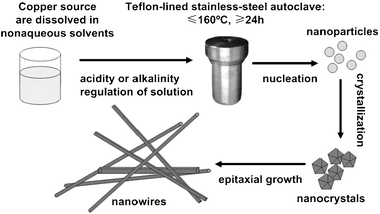 |
| | Scheme 1 Synthetic strategy for the soft-synthesis of single-crystal copper nanowires. | |
The procedure is shown in Scheme 2. SBA-15 powders were prepared according to the literature.17 CuSO4·5H2O (0.066 g) and SBA-15 (0.1 g) were dissolved in distilled water (18 mL) in an Erlenmeyer flask and then aqueous solution was placed under a reduced pressure for 24 h to incorporate metal species into SBA-15 by capillary force. After that the Cu-incorporated SBA-15 was placed into a beaker with 0.5 g of DMAB followed by vigorous mixing for 15 min by a magnetic stirrer. The emulsion was placed in a Teflon-lined stainless steel autoclave of 150 mL capacity. The autoclave was rotated at 40 °C for 7–8 d under autogenous pressure and then allowed to cool to room temperature. The resulting black solution was centrifuged (2000 rpm) or vacuum filtrated and afterwards washed with deionized water and ethanol sequentially. The process was repeated several times to remove the excess surfactant, and a black fluffy solid was obtained. The aim product contains Cu NWs filled in the channels of SBA-15 with diameters around 6–10 nm and lengths below 1 μm, which was kept at room temperature under n-hexane or ethanol.
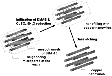 |
| | Scheme 2 Schematic view of the fabrication of copper nanowires from mesoporous silica (SBA-15) as template through nanofilling. | |
2.2 Synthesis of Cu NWs via the ethylene glycol (EG) solvothermal reduction in the presence of PVP
In a typical synthesis, 15 mL of freshly prepared Cu(NO3)2·H2O solution (0.4349 g in EG) was injected into 30 mL of PVP solution (0.675 g in EG) prepared before at a rate of 45 mL h−1 with magnetic stirring. The mixture solution was then kept in a Teflon-lined stainless steel autoclave of 150 mL capacity at a temperature of 160 °C for 24 h. The brownish red precipitate was isolated by centrifugation at 11![[thin space (1/6-em)]](https://www.rsc.org/images/entities/char_2009.gif) 000 rpm, washed several times with distilled water and absolute alcohol, the whole process of reaction was carried out with the protection of nitrogen and the nanowires obtained finally were kept in ethanol at room temperature. The desired product was with diameters within 30–50 nm and lengths vary between 5 and 20 μm.
000 rpm, washed several times with distilled water and absolute alcohol, the whole process of reaction was carried out with the protection of nitrogen and the nanowires obtained finally were kept in ethanol at room temperature. The desired product was with diameters within 30–50 nm and lengths vary between 5 and 20 μm.
2.3 Fabrication of Cu NWs via the glucose hydrothermal reduction in the presence of CTAB
In the steps of the preparation process, we synthesized CuNWs by reducing CuSO4·5H2O (3.144 g) with glucose (2.495 g) in an aqueous solution containing ammonia used to regulate pH = 11. Then CTAB (1.44 g) was added to the water solution followed by vigorous mixing for 0.5 h by a magnetic stirrer until a dark blue emulsion was obtained. The emulsion was added to a reaction flask and heated at 150 °C for 15 h under autogenous pressure. The resulting reddish brown (foxy color) solution was centrifuged (2000 rpm) and then washed with deionized water and ethanol several times sequentially as described above to gather Cu NWs with the diameter between 70–130 nm and lengths longer than 10 μm.
2.4 Characterization of samples
X-Ray diffraction (XRD) detection was carried out on a PANalytical D/max-IIIA XRD instrument operating with Cu Kα radiation (λ = 0.15406 nm). The size, shape, structure and elemental composition of the prepared Cu NWs were measured by scanning electron microscopy (SEM, Netherlands FEI.Co Sirion 200) and energy dispersive X-ray spectroscopy (EDS), respectively. The morphology and the progress of the synthesis were assessed by transmission electron microscopy (TEM; JEM-2100). Samples were sonicated in ethanol before being dropped on a copper mounted holey carbon film and dried. The statistical characterization of the diameter size distribution of each sample was performed based on the TEM images.
3. Results and discussion
3.1 Cu NWs deposit inside SBA-15
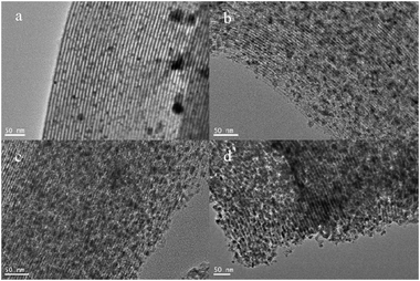
The TEM images of Cu/SBA-15 are shown in Fig. 1c and d. The top surfaces of SBA-15 particles possess many open mesopores (Fig. 1a and b) so that DMAB molecules and Cu ions can infiltrate into the inside of particles. The ordered arrangements of silica mesochannels were well persisted after the Cu deposition. TEM images proved that the Cu nanowires deposited inside the mesochannels were unconnected, and showed a nanowire morphology of about 7–8 nm in diameter corresponding to the mesochannel diameter of the original SBA-15. Interestingly, some of the mesochannels were well filled with Cu NWs for the observed regions in well isolated fragments of SBA-15 particles but some were non-filled in the area of aggregation particles. It is assumed that open mesopores infiltration resistance of aggregation particles is much stronger than that of independent particles, and infiltration of reactants has orientation selectivity in this process. Another observation is that Cu deposition occurs not only at inner parts of particles in the form of nanowires but also on the outer surfaces of SBA-15 particles in the form of Cu nanoparticles or arborization bulk (Fig. 2). It is known that SBA-15 possesses a pore system with completely open mesopores. After introducing Cu with a copper content of >0.0037 g mL−1, due to the limited space of SBA-15, the excessive copper particles located in the pores of SBA-15 and grew along the channels, whereas most of the Cu particles should situate outside the pores.
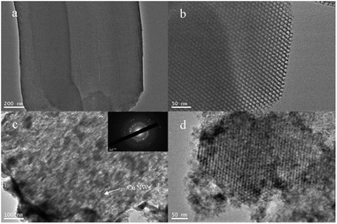 |
| | Fig. 1 (a and b) TEM images of original SBA-15 particles, (c) TEM image of Cu/SBA-15 composite synthetized by vapor infiltration method at 40 °C for 7 d and the inset of (c) is an ED pattern, (d) is a top view of (c). | |
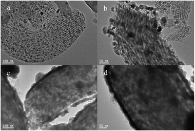 |
| | Fig. 2 TEM images of Cu/SBA-15 composite synthetized with different CuSO4·5H2O concentrations at 40 °C for 7 d: (a) 0.0017 g mL−1, (b) 0.0037 g mL−1, (c) 0.0056 g mL−1, (d) 0.0083 g mL−1. | |
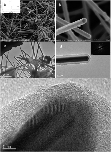
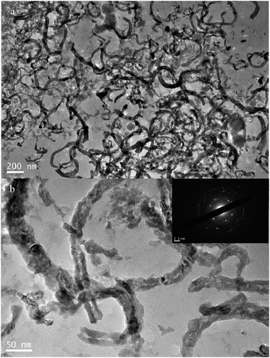
As is well-known, Cu is normally deposited in a manner similar to dendritic growth. Cu crystals grow rapidly along the mesochannels, and it is difficult to fill Cu in the micropores of the walls. Thus, the Cu deposition did not continuously extend to neighboring mesochannels through the micropores but preferably grew along the long axis of the main mesochannels. The products we obtained were about 7–8 nm in diameter and the length of the nanowires was above 1 μm. Cu nanowires synthesized in the present study had bumpy surfaces and low crystallinity due to the mild reduction conditions by vapor infiltration with DMAB. In this case, copper nanocrystals grow slowly which is strongly related to the low reaction temperature. As shown in Fig. 3 that in different reaction stages the filling quantity in mesopores of SBA-15 is markedly different, which revealed that the aspect ratios of the replicated copper nanowires were controlled by the applied reduction time. When the reduction lasted for 1 d, Cu nanoparticles of about 5–6 nm in diameter were mainly observed (Fig. 3a). As the reduction time increased, the Cu nanoparticles became longer to form nanowires. And these TEM images also proved that the crystal growth absolutely proceeds only along the mesochannels without connection to neighbors due to high confinement of crystal growth by rigid silica walls. It is interesting to note that different mesoporous materials with various pores exhibit quite different dispersion behaviors of the disperse guest species. In I3K-templated silica nanotubes after calcinations samples developed by Hai Xu et al.18 were with the same CuSO4·5H2O content of 0.0037 g mL−1, the guest can be well-dispersed on the surface of these templates as shown in Fig. 4. Unlike Cu deposit in templates' channels of SBA-15, Cu particles tend to wrap the outside of these silica nanotubes to form nanowires with bending (Scheme 3). Finally the copper nanowires with an outer diameter in the range of 9–11 nm and an inner diameter of ∼4 nm are easily determined.
 |
| | Fig. 3 TEM images of Cu/SBA-15 for (a) 1 day, (b) 2 days, (c) 4 days, and (d) 7 days of reduction. All scale bars show 50 nm in length. | |
 |
| | Fig. 4 TEM images of Si NTs@Cu composite synthetized by vapor infiltration method at 40 °C for 7 d, (b) is a highly magnified image of selected area of (a) and the inset of (b) is an ED pattern. | |
These results provide solid experimental evidence for the growth mechanism of uniform copper nanowires in the vapor infiltration process in the presence of DMAB. However, adsorptive desulfurization within channels of the SBA-15 method have a fault that preparation time is long which is a predominant influence of preparation efficiency, the yield is unsatisfied and the products can be easily oxidized in the atmosphere. Since this present solution synthesis method of copper nanowires involve nucleation, seeding, and growth or filling, we believe that these findings might inspire other advantageous solution synthesis systems of copper nanostructures with high crystallinity, efficiency, low-cost and high yield similarity.
3.2 Cu NWs generated by a polyol-thermal approach
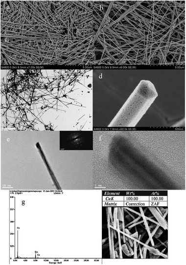
Fig. 5 shows the SEM images of synthesized products, there are 30% nanoparticles observed in the product separated by centrifugation at 2000 rpm (Fig. 5a), and a high yield of the product improved to 90% by increasing centrifugal rate up to 10000 rpm (Fig. 5b). The average diameter of Cu NWs is 40 nm, and their lengths vary between 5 and 20 μm. It is clearly revealed from the inset in Fig. 5e that the shapes of copper nanowires make a complete pentagonal prism. The composition of the products was examined by EDAX, and the results indicate that copper nanowires and nanoparticles in all samples with the protection of n-hexane were not oxidized by air. The crystallographic structure of one tip of an individual nanowire was identified using HRTEM in order to further understand more details of the microstructure. Fig. 5f shows the HRTEM image of a 5-fold symmetry structure at the end of a nanowire which indicates that a similar lattice fringe distance of 0.21 nm corresponds to the d value for (111) planes of face-centered-cubic (fcc) copper.19 According to the selected area electron diffraction (SAED) obtained with the beam parallel to the [110] axis shown in Fig. 5, it is known that the copper nanowire is crystallized and is a single crystal because the diffraction spots could be assigned to any particular simple pattern associated with the fcc copper crystal.
In a typical polyol synthesis, copper atoms are obtained by reducing Cu(NO3)2 with the lone pair electron of the oxygen atom on the carbonyl formed from ethylene glycol (EG) through reactions (1) and (2).
| | | 2HOCH2–CH2OH → 2CH3CHO + 2H2O | (1) |
| | | Cu2+ + 2CH3CHO → CH3CO–OCCH3 + Cu + 2H+ | (2) |
First, during the nucleation period once the concentration of
copper atoms has reached the supersaturation value, they will start to nucleate and grow into
nanoparticles. At the same time, HNO
3 generated
in situ will dissolve the formed solid
copper particles so that the balance of
precipitation–dissolution will appear as shown through
reaction (3)| | | 3Cu + 8HNO3 ↔ 3Cu(NO3)2 + 2NO + 4H2O | (3) |
Second, as the reaction continued, HNO
3 is gradually consumed and a second round of nucleation occurs and these
nanoparticles grew into either a single-crystalline or twinned morphology. The twinned particles were sensitive to
etching of HNO
3 because of lower surface energy and they were distorted easily in the solvothermal system. The
rest more stable seeds can continue to grow into single-crystalline morphology as expected.
In the ultimate stages of the reaction, the Cu nanoparticles formed in the first two stages were well-dispersed in the absence of PVP because of the chemical adsorption onto the surface of solid copper through bonding between polymeric surfactant molecule and Cu as shown in Scheme 4. As is well known that for the fcc metals (e.g. Au, Ag, and Cu), the {110} facets are the least stable among the three (111, 110 and 100), the growth rate of {110} facets should be much faster in the absence of templates (PVP).20 The free energy minimization and the stronger surface interaction of the PVP molecule with Cu {100} could result in preferential adsorption onto [100] planes of the Cu nanoparticles, leading to the prior kinetic growth along the [110] direction and further resulting in the formation of five-twinned nanowires due to limited growth along the [100] direction. Overall, PVP plays an important role in controlling the growth rates of different crystalline faces and leading to a highly anisotropic growth as templates.
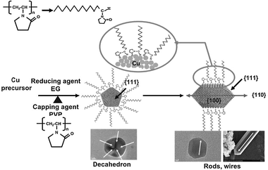 |
| | Scheme 4 Schematic illustration of the shape evolution process of copper crystals with the increasing reaction time. | |
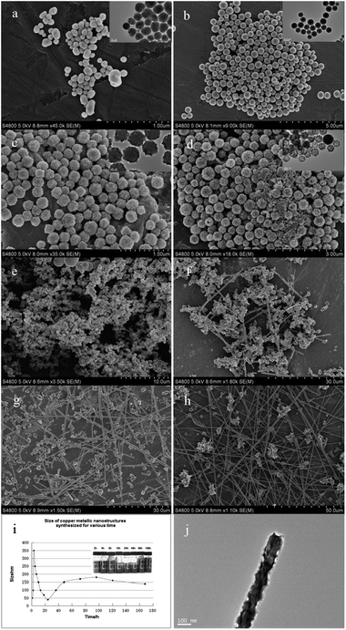
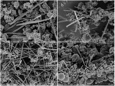
In this system, the growth process of single-crystal copper nanowires is a kinetically and thermodynamically controlled process that can form different final shapes with some degree of shape tunability through changes in the PVP concentration, reaction temperature, and reaction time. Fig. 6 shows SEM images of Cu nanostructures obtained at 160 °C for 24 h using different weights of PVP. It can be clearly seen that final products transformed from nanowires into nanoparticles and nanospheres when PVP concentration was more than 9 mM, meanwhile, these copper nanowires obtained are well-defined and the morphology of products becomes uniform, and the wire surface becomes smooth with an increase in PVP concentration. Fully developed copper nanowires from octahedra or decahedron nanoparticles were formed with the narrow size distribution that is measured to be about 50–90 nm when the PVP concentration is 4.5 mM. Upon increasing the PVP concentration to 9–13.5 mM, most loose spherical particles with rough surfaces were obtained, the particles are monodispersed with a diameter of 400–500 nm. According to the test results, spherical particles are generated only when the PVP concentration is more than 8 mM, the reason is that the high coverage of PVP on all the planes of copper nanocrystals leads to an isotropic growth. These previously-prepared nanoparticles will affect the size and morphology of nanowires ultimately. Generally, it can be indicated that PVP controls the size, morphology and homogeneous degree of final products in this reaction progress.
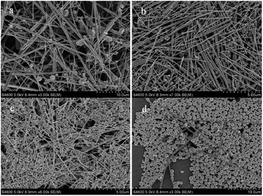 |
| | Fig. 6 SEM images of final products obtained at 160 °C for 24 h using different concentrations of PVP: (a) 2.25 mM, (b) 4.50 mM, (c) 9.00 mM, (d) 13.50 mM. | |
The influence of reaction temperature on the formation of Cu NWs was also investigated, at 140, 160, 180 and 200 °C for 24 h using 4.5 mM PVP (Fig. 7). The reaction temperature affects not only the reaction activity but also the nucleation and growth rates of nanowires. When the temperature is below 160 °C for more than 16 h there is no or a small amount of nanowires but most cubic nanoparticles obtained, with a further increase of the reaction temperature to 180 °C and 200 °C, many ill-defined aggregates and blocks are observed in addition to well-developed nanowires due to high reaction rate. It seemed that the relatively low reaction temperature could not provide enough energy required for the dissolution and the diffusion of PVP molecules on the surface of copper nanorods or nanowires for the anisotropic growth, inversely higher temperature leads to rise of system internal energy and capping agent became hyperactive to hinder the adsorption on the surface of copper nanorods. And above all, the morphology and transformation of the nanowires in this system are very sensitive to temperature changes.
 |
| | Fig. 7 SEM images of final products synthesized at different temperatures for 24 h: (a) 140 °C, inset of (a) is TEM of some nanoparticles, (b) 160 °C, (c) 180 °C, (d) 200 °C. | |
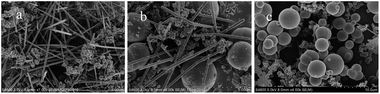
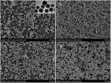
For a complete view of the formation process, we consider the growth process of Cu NWs when using 5 mM PVP at 160 °C by interrupting the reaction in different stages of 2 h, 3 h, 5 h, 7 h, 10 h, 13 h, 18 h, and 24 h. When the reaction is carried out for 2 h, all of the products are uniform nanocrystals within 150 nm (Fig. 8a). After a reaction time of 3 h, all of the nanoparticles transformed into nanospheres within 500 nm (Fig. 8b). Upon increasing reaction time to 5–7 h it was found that all the nanospheres became coarse and hollow structured, their mean diameters reduced to 150–200 nm (Fig. 8c and d). Presumably, when the reaction proceeds for 10–13 h, the nanoparticles coagulated into irregular lump with the extension of crystallization time (Fig. 8e). Meanwhile, certain amounts of prism-shaped nanowires with an average diameter of about 200 nm and lengths longer than 10 μm begin to appear from coagulated particles, but the homogeneity and productivity of products are unsatisfactory (Fig. 8f). In particular, the diameter of nanowires reduced to 130–150 nm but the yield increased slightly when the reaction time is further increased to 18 h (Fig. 8g). As was expected according to the time-dependent morphology performed, the yield of the nanowires improved when the reaction time was increased to 24 h (Fig. 8h), however, the surface defect of some nanowires as sawtooth appeared. From the size statistics curve diagram we may safely draw the conclusion that the size of copper metallic nanostructures accreted at first and then decreased until steady during the development process of nanowires, and with the increasing ageing time to 4–5 d the size of nanowires reduced slightly due to the aggrandization of surface defects by etching of the poly-thermal system (Fig. 8i and j).
 |
| | Fig. 8 SEM images of samples at different stages of polyol-thermal treatment (a) 2 h, (b) 3 h, (c) 5 h, (d) 7 h, (e) 10 h, (f) 13 h, (g) 18 h, (h) 24 h, and inset are in situ TEM observation of (a–d), respectively, to investigate these nanoparticles inner structure. (i) Size statistics curve diagram of copper nanostructures obtained by different reaction stages, (j) defects on the surface of a nanowire investigated by TEM. | |
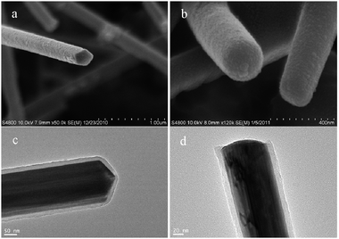
In order to ascertain the reason why these products were not easy to undergo oxidation, we examined the nanowire internal structure with transmission electron microscopy (TEM) (Fig. 9c). The investigation of TEM and EDS, TEM images shows that all the prepared copper samples have a thin carbonaceous layer (a thickness of 7–20 nm) on the surface of the wire, which can prevent oxygenation in air. Fig. 9e shows the HRTEM image of the inner copper nanowires. The fringe pattern of the nanowires indicates a spacing of 2.07 Å, corresponding to the (111) plane of copper. The inset image of Fig. 9d shows a selected area electron diffraction (SAED) pattern. This pattern indicates that the electron beam is oriented along the [110] zone axis, and that the nanowire consists of a single-crystalline domain.
The formation of Cu@C core–shell structured nanowires involved two primary stages as shown in Scheme 5: nucleation of inner copper nanowires and consequent epitaxial growth and thickening of the carbonaceous shell on the inner core.
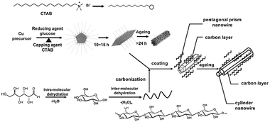 |
| | Scheme 5 Mechanism for the formation of Cu@C nanowires and transition of the shape from pentagonal prism to cylinder with the aging time. | |
The formation of metallic copper nanowires in this work is based on the following redox reaction under the basic conditions. According to copper mirror reaction:
| | | C6H12O6 + Cu(NH3)2(OH)2 → C5H11O5COONH4 + Cu + NH3 + H2O | (4) |
Meanwhile, with an increase in temperature (>120 °C)
glucose loses
water first through an intramolecular
condensation reaction as a result of its stable pyranose structure and then further intermolecular dehydration generates carbonaceous shell according to the
La mer model,
21 then they began to deposit on the different faces of the
copper particles to reduce the total surface energies and form a carbonaceous layer coated on the surfaces of
copper particles partially or completely. And
CTAB assisted
growth led to well-crystallized pentagonal
nanowires. In this progress, the use of
CTAB which can react with the
copper ion to form the stable intermediate [Cu(CTAB)
2]
2+ is critical for the formation of the
copper nanowires. And the possible chemical reaction producing the
copper nanowires is:
| | | [Cu(CTAB)2]2+(aq.) + 4OH−(aq.) + 2C5H11O5–CHO → Cu + 2CTAB + 2H2O + 2C5H11O5–COOH | (5) |
The
amine groups of
CTAB allow it to bind onto the surface of
copper nanostructures in solution. If
CTAB binds preferentially to the side facets of the CuNWs, this could cause preferential
growth along the axial [110] direction. Finally, the interaction between the functional
groups in the carbonaceous shell and the surface of the
copper core was achieved
via a simple one-step reaction. As carbonaceous deposition continues more and more edges and corners appear, which lead to transformation from pentagonal prism Cu@C NWs (
Fig. 10a and c) to cylindrical Cu@C NWs (
Fig. 10b and d).
 |
| | Fig. 10 SEM images of Cu@C nanowires with the reaction time (a) 15 h and (b) 24 h, (c and d) are in situ TEM observation of (a and b) respectively. | |
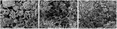
In a typical process of synthesis, the experimental results show that the ratio of glucose to CuSO4·5H2O, amount of CTAB, reaction temperature and crystallization time are necessary for the product yield and morphology of the final product structures. At the molar ratio of glucose/copper 1:1 (Fig. 11a), mostly nanowires were formed but at high glucose contents such as at the ratio of glucose/copper 3:1 or 4:1 (Fig. 11b and c), the products transformed into carbonaceous micro-spheres with a diameter in the range of 300–600 nm because copper seeds cannot breakthrough the sugar-coat to form nanowires. Reversely, decreasing the amount of glucose will lead to incomplete reduction of copper ions.
Samples a, b, c, and d correspond to 0.5 g, 1.0 g, 1.5 g, and 2.0 g of the original CTAB amount (Fig. 12). As the amount of CTAB was increased from 0.5 g to 1.5 g, the diameter of the nanowires decreased from 400 nm to 150 nm, while the length increased from 4 μm to 10–20 μm, and that, much higher concentration of CTAB will create micella which gives rise to flocculation. This result suggests that appropriate concentration of CTAB preferentially plays a role in leading to anisotropic growth of ultralong nanowires. To examine temperature effect on growth of Cu NWs, the ratio of reactants was fixed as 1:1, reaction time was fixed as 15 h and the temperature was changed from 120 °C to 170 °C. The products were the flowerlike nanoparticles (Fig. 13a) due to the lower activity of the system when the temperature was below 120 °C, but molecular motion is more intense if the temperature is increased up to 170 °C that makes the adsorption of CTAB unstable on the (100) crystal surface and the yield of nanowires is also unsatisfactory. Moreover, the nanowires obtained at 170 °C are totally bending to reduce the intrinsic energy compared with products received at 150 °C (Fig. 13b and c). Since the growth mechanism of copper nanowires is fully understood, it is not difficult to comprehend the dissolution of CTAB with the extension of duration time which is necessary to promote anisotropic growth of Cu NWs, which plays an important role in getting high purity and good uniformity nanowires.
 |
| | Fig. 12 SEM images of Cu@C nanowires synthesized at 150 °C for 15 h with different amounts of CTAB: (a) 0.5 g, (b) 1.0 g, (c) 1.5 g and (d) 2.0 g. | |
 |
| | Fig. 13 SEM images of Cu@C nanowires synthesized at different temperatures: (a) 120 °C, (b) 150 °C, and (c) 170 °C. | |
4. Conclusions
In summary, a series of scales of copper nanowires has been synthesized through a soft synthesis method. Recent advances demonstrate that these “soft” approaches give several very promising alternative pathways for the fabrication of low-dimensional nanocrystals such as nanowires, nanorods and more complex nanostructures. Among the solution strategies we have described in the article, the solvothermal/hydrothermal process shows the potential capabilities for selective preparation of copper nanowires of varying diameters with controllable morphology, dimensions and composition under mild conditions. And these new development methods have more comparative advantages and market potential compared with “hard” approaches because of their low-cost, lower energy consumption and reduce pollutants discharge. However, critical factors for the synthesis of high-quality nanowires such as nucleation, crystallization, self-assembly, and growth mechanism of the nanocrystals are still not completely understood. Furthermore, there are still some problems at the present time, for instance there is no effective method for the determination of the single nanowire electrical property, optical performance, thermodynamic stability and mechanical property. From the viewpoint of applications, investigation of the relationship between the morphology and properties is of crucial and imperative significance after a high preparative performance low temperature liquid-phase method was discussed. And these new found will result in developing new applications of building blocks in nanoscience and nanotechnology.
Acknowledgements
This work is supported financially by the National Natural Science Foundation of China (Grant No. 50901090).
Notes and references
- A. Takai, Y. Doi, Y. Yamauchi and K. Kuroda, Soft-Chemical Approach of Noble Metal Nanowires Templated from Mesoporous Silica (SBA-15) through Vapor Infiltration of a Reducing Agent, J. Phys. Chem. C, 2010, 114, 7586–7593 CrossRef CAS.
- S. Chang, K. Chen, Q. Hua, Y. Ma and W. Huang, Evidence for the Growth Mechanisms of Silver Nanocubes and Nanowires, J. Phys. Chem. C, 2011, 115, 7979–7986 CrossRef CAS.
- M. Tsuji, K. Matsumoto, N. Miyamae, T. Tsuji and X. Zhang, Rapid Preparation of Silver Nanorods and Nanowires by a Microwave-Polyol Method in the Presence of Pt Catalyst and Polyvinylpyrrolidone, Cryst. Growth Des., 2007, 7(2), 311–320 CrossRef CAS.
- W. Yang, L. Qu, R. Zheng, Z. Liu, K. R. Ratinac, L. Shen, D. Yu, L. Yang, C. J. Barrow, S. P. Ringer, L. Dai and F. Brae, Self-Assembly of Gold Nanowires along Carbon Nanotubes for Ultrahigh-Aspect-Ratio Hybrids, Chem. Mater., 2006, 4, 9.
- K. R. Krishnadas, P. R. Sajanlal and T. Pradeep, Pristine and Hybrid Nickel Nanowires: Template-, Magnetic Field-, and Surfactant-Free Wet Chemical Synthesis and Raman Studies, J. Phys. Chem. C, 2011, 115, 4483–4490 CrossRef CAS.
- J. L. Duan, T. W. Cornelius, J. Liu, S. Karim, H. J. Yao, O. Picht, M. Rauber, S. Muller and R. Neumann, Surface Plasmon Resonances of Cu Nanowire Arrays, J. Phys. Chem. C, 2009, 113, 13583–13587 CrossRef CAS.
- P. Dua, S. Sharma and P. Kumar, Density Functional Study of 1D Nanowire for Biomedical Applications, J. Biomed. Nanotechnol., 2011, 7(1), 93–94 Search PubMed.
- Y. Feng and X. Zheng, Plasma-Enhanced Catalytic CuO Nanowires for CO Oxidation, Nano Lett., 2010, 10, 4762–4766 CrossRef CAS.
- J. Liu, Y.-C. Son, J. Cai, X. Shen, S. L. Suib and M. Aindow, Size Control, Metal Substitution, and Catalytic Application of Cryptomelane Nanomaterials Prepared Using Cross-linking Reagents, Chem. Mater., 2004, 16, 276–285 CrossRef CAS.
- C. He, P. Zhang, Y. F. Zhu and Q. Jiang, Structures and Quantum Conduction of Copper Nanowires under Electric Fields Using First Principles, J. Phys. Chem. C, 2008, 112, 9045–9049 CrossRef CAS.
- M. Adachi, Y. Murata, J. Takao, J. Jiu, M. Sakamoto and F. Wang, Highly Efficient Dye-Sensitized Solar Cells with a Titania Thin-Film Electrode Composed of a Network Structure of Single-Crystal-like TiO2 Nanowires Made by the “Oriented Attachment” Mechanism, J. Am. Chem. Soc., 2004, 126, 14943–14949 CrossRef CAS.
- W.-T. Yao, S.-H. Yu, Y. Zhou, J. Jiang, Q.-S. Wu, L. Zhang and J. Jiang, Formation of Uniform CuO Nanorods by Spontaneous Aggregation: Selective Synthesis of CuO, Cu2O, and Cu Nanoparticles by a Solid–Liquid Phase Arc Discharge Process, J. Phys. Chem. B, 2005, 109(29), 14011–14016 CrossRef CAS.
- G. F. Iriarte, Growth of nickel disilicide nanowires by CVD, J. Non-Cryst. Solids, 2010, 356, 1135–1144 CrossRef CAS.
- G. Malandrino, S. T. Finocchiaro, R. L. Nigro, C. Bongiorno, C. Spinella and I. L. Fragalà, Free-Standing Copper(II) Oxide Nanotube Arrays through an MOCVD Template Process, Chem. Mater., 2004, 16(26), 5559–5561 CrossRef CAS.
- Y. Shimotsuma, T. Yuasa, H. Homma, M. Sakakura, A. Nakao, K. Miura, K. Hirao, M. Kawasaki, J. Qiu and P. G. Kazansky, Photoconversion of Copper Flakes to Nanowires with Ultrashort Pulse Laser Irradiation, Chem. Mater., 2007, 19(6), 1206–1208 CrossRef CAS.
- R. Kitaura, R. Nakanishi, T. Saito, H. Yoshikawa, K. Awaga and H. Shinohara, High-Yield Synthesis of Ultrathin Metal Nanowires in Carbon Nanotubes, Angew. Chem., 2009, 121, 8448–8452 CrossRef.
- D. Zhao, J. Feng, Q. Huo, N. Melosh, G. H. Fredrickson, B. F. Chmelka and G. D. Stucky, Triblock Copolymer Syntheses of Mesoporous Silica with Periodic 50 to 300 Angstrom Pores, Science, 1998, 279, 548–552 CrossRef CAS.
- H. Xu, Y. Wang, X. Ge, S. Han, S. Wang, P. Zhou, H. Shan, X. Zhao and J. R. Lu, Twisted Nanotubes Formed from Ultrashort Amphiphilic Peptide I3K and Their Templating for the Fabrication of Silica Nanotubes, Chem. Mater., 2010, 22, 5165–5173 CrossRef CAS.
- D. G. Dempsey and L. Kleinmanm, Structural stability and lattice defects in copper: ab initio, tight-binding, and embedded-atom calculations, Phys. Rev. B: Solid State, 1977, 16, 5356–5366 CrossRef CAS.
- Z. Wang, Y. Li and J. B. Adams, Kinetic lattice Monte Carlo simulation of facet growth rate, Surf. Sci., 2000, 450, 51–63 CrossRef CAS.
- V. K. LaMer and R. H. Theory, Production and Mechanism Of formation Of Monodispersed of hydraulic oil, J. Am. Chem. Soc., 1950, 72(11), 4847–4854 CrossRef CAS.
Footnote |
| † Electronic supplementary information (ESI) available. See DOI: 10.1039/c1nj20800d |
|
| This journal is © The Royal Society of Chemistry and the Centre National de la Recherche Scientifique 2012 |
Click here to see how this site uses Cookies. View our privacy policy here.