Joining plasmonics with microfluidics: from convenience to inevitability†
Jaeyoun
Kim
*
Department of Electrical and Computer Engineering, Iowa State University, Ames, Iowa, 50011, USA. E-mail: plasmon@iastate.edu; Tel: 1-515-294-4214
First published on 3rd August 2012
Abstract
Along the advances in optofluidics, functionalities based on the surface plasmon-polariton have also been finding an increasing level of involvement within micro/nano-fluidic systems, gradually forming a new field of plasmo-fluidics. This survey of the burgeoning field reveals that judicious selection and combination of plasmonic and micro/nano-fluidic features render the plasmo-fluidic integration useful and mutually beneficial to the point of inevitability. We establish categories for the level of integration and utilize them as a framework for surveying existing work and extracting future perspectives.
 Jaeyoun Kim | Jaeyoun Kim received his Ph.D. in Electrical Engineering from the University of Michigan at Ann Arbor in 2003. He then joined Professor Luke P. Lee's BioPOETS Lab at the University of California at Berkeley as a postdoctoral researcher. There he studied optofluidics, plasmonics, and biomimetic optical devices. In 2006, he joined the Electrical and Computer Engineering Department of Iowa State University where he is currently an Associate Professor. His current research topics include bio-inspired microsystems, plasmonic photovoltaic devices, and bio-photonic sensors. He was the recipient of NSF’s CAREER award in 2010 and Air Force Summer Faculty Fellowship in 2009. |
1. Introduction
The simultaneous rise of plasmonics and microfluidics during this century's first decade was more of an inevitable consequence than a coincidence. Amid the burst of the biggest bubble in the history of technology, the fields of optics and MEMS, both forerunners in the high-tech race, were in desperate search for areas of new application and sources of continued innovations. There then came the rapid influx of nanotechnology and unconventional microfabrication. With those in hand, researchers in the fields enthusiastically explored plasmonic sub-wavelength optics and rapid-prototyping of lab-on-a-chip devices. Almost immediately, the two streams of research met each other in the field of bioengineering and formed a new branch that can best be named plasmo-fluidics. Reports on this plasmo-fluidic integration date as far back as 1991 and their rapid progress and ramification, illustrated in Fig. 1, call for a technical survey. | ||
| Fig. 1 Organization chart with the survey topics arranged in accordance with the proposed framework of categorization. | ||
At the interface between metallic and dielectric materials, an optical wave in the dielectric side can initiate a periodic fluctuation in the metal's charge density. An evanescent wave also appears in the dielectric side, linking the positively and negatively charged areas. If a set of resonance conditions were satisfied, this evanescent wave can be phase-matched to the original excitation wave and the fluctuation in the charge density can be sustained. Such a resonantly coupled state of charge density fluctuation and optical waves is commonly referred to as the surface plasmon-polariton (SPP). Depending on the geometry and dimensions of the metallic hosting structure, the SPP can take either a propagating (P-) or localized (L-) form, giving rise to a P- or L-SPP, respectively. For planar, unbound metal-dielectric interfaces, the P-SPP is the dominant form, although its excitation requires strict phase-matching through the use of Otto or Kretschmann setup. Fig. 2a schematically illustrates the optical excitation of P-SPP using the results of numerical simulations. On the other hand, the L-SPP develops around metallic structures that are small with respect to the wavelength of the optical wave, as shown Fig. 3a. Regardless of the type, the optical wave portion of the SPP, shown schematically in Fig. 2b, enjoys benefits such as localization below the diffraction-limit and dramatic intensity enhancement in the direct vicinity of the interface. The former comes from the wave's evanescent nature and the latter from the extremely tight confinement of electrons within thin and/or small metallic regions. Thanks to the involvement of highly interactive electrons, the SPPs can couple with each other much more actively than purely optical waves could, resulting in a wealth of hybrid modes. Best of all, the efficiencies associated with these plasmonic phenomena depend strongly on the nanoscale dielectric environment of the metallic hosting structure, providing facile routes for optical biosensing at molecular levels.
 | ||
| Fig. 2 (a) Numerical simulation results of failed (upper) and successful (lower) excitation of P-SPP. The P-SPP field profile above the Au layer clearly reveals its evanescent nature. (b) A schematic view of the electric fields associated with the charge density fluctuation. Again, the evanescent nature is evident with sub-micron tail extent. (c) A typical setup for plasmo-fluidic SPR and SPRi with microfluidic systems integrated directly over the phase-matching prism. Reproduced from ref. 9. (d) An example of critical-level-integrated SPRi device comprising multi-well array with a matching reconfigurable valve system. Reproduced from ref. 9. | ||
 | ||
| Fig. 3 (a) A schematic diagram explaining the physical origin and optical characteristics of L-SPP developed around a metallic nanostructure (MNS). (b) A plasmonic nanohole-based biosensor for use in the flow-through configuration. The transmission-based detection allows the adoption of a collinear arrangement in which the light source and the detector can be placed on opposite sides across the nanohole sensor. (c) A plot showing the superiority of the flow-through configuration over the flow-over one in terms of time response. (b) and (c) reprinted with permission from ref. 32. Copyright (2009) American Chemical Society. | ||
Dielectric materials in the liquid phase also offer features useful for optical applications. Thanks to their fluidic nature, they can create a perfectly conformal dielectric environment around an optical component simply by surrounding it. The same fluidic nature also enables rapid and dynamic modification of the dielectric environment through injection and/or mixing of liquids exhibiting different dielectric characteristics. The level of the resulting refractive index change greatly exceeds those attainable through electro-, acousto-, or nonlinear optical methods.1 The microfluidic architecture further strengthens these advantages with its tight fluidic confinement and precise fluidic control at a length-scale ideally matching those of integrated optic components, such as waveguides and resonators. Microfluidically confined liquid can also exert a physical force on microstructures in its way, enabling their actuation and transport. Interestingly, liquid medium also provides forces countering externally applied ones, such as the fluidic drag force in microscale and Brownian motion in nanoscale. These can be exploited to our advantage, most notably for refining particle motions in liquids.
Early stage plasmo-fluidic integration started out with in-channel implementations of SPP-based biosensing, a logical target with self-evident technical advantages. As shown in Fig. 2b, in the dielectric side, the SPP's electric fields are evanescent with only ∼300 nm extent above the metal-dielectric interface. Since the reagents and analytes in the volume beyond the SPP's extent would simply be wasted, the use of low-profile microfluidic channels for their delivery made a perfect sense. The fact that the extra volume, while not contributing to signal generation, can still obscure the measurement by casting temperature and/or concentration gradient further strengthen the plasmo-fluidic integration's benefit,2 most notably in the SPP-based studies of molecular interaction kinetics in which the diffusion rate is the main factor.3 The use of optical waves which requires no shielding or insulation proved ideal for liquid-based sensing tasks as well. This type of straightforward co-utilization of plasmonic and microfluidics features has led to the first stage of plasmo-fluidic integration that can be named convenience-level integration. The length-scale of microfluidic structures, typically measured in microns, and their easy patterning have been the main targets of exploitation at this level.
With the research growing both in size and diversity, such intuitively obvious integration has gradually evolved into more sophisticated ones. This new stage of integration is marked by the proactive search for useful yet unexploited functionalities in microfluidics or plasmonics and their utilization to bring in significant enhancements to their counterparts. The process usually involves substantial modification of the original configuration and/or the introduction of extrinsic techniques or materials. This phase can be named convergence-level integration. In both the convenient- and convergence-level integrations, reconciling the fundamental difference in the plasmonic and microfluidic length-scales, one measured in nm while the other in microns, remains the biggest challenge.
Recently, the integration has further progressed into a higher level at which totally new plasmo-fluidic functionalities are created with the combined use of microfluidics and plasmonics presumed from their very conception. In this case, the plasmo-fluidic integration becomes inevitable. On the other hand, as the plasmo-fluidic device miniaturized towards the nanoscale, the plasmonic and microfluidic effects become difficult to separate as well, whether intended or not. Critical-level may be an adequate term to label this phase. At this level, the challenge has been extended to the separation of the two inseparable functionalities, for their better design and analysis. Of course, there are numerous emerging research outcomes whose levels of integration are yet to be determined.
In this review, we survey the recent progress in plasmo-fluidics using the framework of convenience-convergence-critical level categorization and try to extract future perspectives from the emerging ones. Areas and sub-areas of plasmo-fluidics to be reviewed are summarized in Fig. 1 along with their typical length-scales. They stem from three major types of SPPs, i.e., P-SPP, L-SPP, and LR (long range)-SPP, and branched into different sub-areas in response to demands and technical limitations. Microfluidic synthesis of plasmonic nanostructures is also to be surveyed using the same framework for completeness.
2. SPR for plasmo-fluidic integration
In this section, we will apply the aforementioned framework to the most deep-rooted and widespread branch of plasmo-fluidics, the surface plasmon resonance (SPR) biomolecule sensing and imaging, as an introductory example. The term SPR refers to the resonant excitation of P-SPP by an optical wave with the phase-matching between them achieved through the use of a prism or a grating. Many miniaturization schemes in SPR involve convenience-level plasmo-fluidic integration. In those schemes, microfluidic channels are fabricated or installed directly over the phase-matching prism or grating, as shown in Fig. 2c, providing an apparent reduction in the sensing volume and a simple yet controlled means for sample delivery.4,5 A recent report even described the integration of grating-based SPR with a compact disc-type microfluidic system which utilizes inertial force to facilitate sample transport and optical read-out.6Soon these evolved into a convergence-level integration in which features specific to microfluidics were proactively exploited. The laminar nature of the microflow was the first target. Providing an on-chip self-reference has been an important goal, especially for the realization of differential SPR sensing schemes, and the microfluidic system's capability to form a set of co-propagating flows in their channels proved ideal for its accomplishment.7 A more complex functionality, the microfluidic chemical signal generation, has also been integrated with SPR. Through microfluidic synthesis of chemical signals, the impacts of noise and background thermal drift could be mitigated, leading to a substantial decrease in the minimum detection limit.8 In these convergence-level examples, the microfluidics functionalities played active roles to improve the performance of the plasmonic counterparts.
It is the advent of SPR imaging (SPRi) which rendered the plasmo-fluidic integration inevitable, eventually leading it to the critical level. SPRi pursues parallel processing of SPR using a broadly collimated excitation beam, an array of sample reservoirs, and a wide field-of-view camera in combination. With high throughput, real-time monitoring, and process automation set as the main technical goals,9 the use of microfluidic architectures and functionalities is a must, not an option. The microfluidic devices in the SPRi setups can be subcategorized into multi-functional or multi-layered ones. The former focuses on maximizing the process automation and achieves it by installing as many microfluidic functionalities as possible. For instance, Lee et al. integrated microscale pumps, valves, flow sensors, heaters, and temperature sensors along with passive channels and reservoirs.10 Krishnamoorthy et al. also integrated on-chip generators of electro-osmotic and electro-kinetic flows.11 On the other hand, the multi-layered microfluidics focuses on realizing dynamically reconfigurable and/or individually addressable sample array patterns. The use of crossed flow channels,9,12 microfluidic printing,13 and 3D flow cell arrays14 all fall in this subcategory and are now indispensable in SPRi. Fig. 2d shows the reconfigurable microfluidic SPRi by Luo et al.9
Currently, the biggest challenge in plasmo-fluidic SPR is the growing complexity in the microfluidic subsystems, especially for those intended for on-demand reconfiguration. New microfluidic techniques are demonstrated to address the issue. Recent advances in droplet-based microfluidics and electro-wetting actuation have been immediately adopted for dynamically reconfigurable SPRi pattern generation and referencing.15 The utilization of SPR for profiling nanofluids in microfluidics channels16 is of special interest since the direction of benefit, which usually flows from microfluidics to plasmonics, was reversed in this case. To which level these emerging applications should be categorized will be determined as their uses expand. This section also validates the proposed survey framework.
There have also been efforts to find the optimum microfluidic length-scale in the plasmo-fluidic SPR and SPRi. The analysis by Gervais and Jensen17 and Squires et al.18 revealed that the efficiency of SPR- or SPRi-based molecule detection in microfluidic settings depends on the interplays between convection, diffusion, and surface-bound reaction. Their relative strengths are signified by two Peclet numbers (PeH and PeS, the channel and sensor Peclet number, respectively) and Damköhler number (Da). The Peclet numbers represent the relative thickness of the depletion layer with respect to the channel and sensor size, respectively. On the other hand, Da indicates the relative strength of diffusion and surface-bound reactions. In typical microfluidic settings, the channel height h becomes the most critical parameter governing these ratios. Shallow channels, with h ∼ 1 μm, can drive the operation into the diffusion-dominant, surface reaction-limited regime. The low channel profile also better matches the short extent of the P-SPP's evanescent tail. For microfluidic channels made with elastomers such as PDMS, however, the sagging of the channel ceiling towards the floor also needs to be considered. The empirical rule is to avoid any channel aspect ratio greater than 20![[thin space (1/6-em)]](https://www.rsc.org/images/entities/char_2009.gif) :1,19 which sets the minimum channel height at a typical value of 10 μm.
:1,19 which sets the minimum channel height at a typical value of 10 μm.
3. Localized SPP for plasmo-fluidic integration
The L-SPP arises when an optical wave drives the electrons within a nanoscale metallic structure resonantly, as shown in Fig. 3a. It manifests itself by modifying the reflection or transmission of the excitation wave. The L-SPP-based biosensing setup can be simpler than those for SPR since the former does not require phase-matching. The L-SPP excitation condition, however, is still a sensitive function of the nanostructure's dielectric environment, enabling us to track molecular interactions in the direct vicinity of metallic nanostructures by monitoring the change in the L-SPP excitation efficiency or, equivalently, the change in the excitation wave's reflection or transmission. The extent of the L-SPP's evanescent wave on the dielectric side is often shorter than that of the P-SPP, sometimes less than 100 nm. Such a tight localization of optical energy is beneficial for amplifying the electric field but also leads to the inevitable reduction in the sensing volume. For this reason, bringing the analyte molecules within the sensing volume of the L-SPP, usually a thin shell around the metallic nanostructure, has often been a bigger issue than the sensing itself and has become the most significant challenge. Through numerical modeling, Sipova et al. showed the inferiority of L-SPP to P-SPP in detecting surface-specific binding events in the presence of microflow, which hinders the transport process.203.1 Convenience- and convergence-level integrations
The plasmo-fluidic integration for L-SPP-based biosensing has long been at the convenience-level with the microfluidic portion functioning as spatially confining conduit of analytes. The effort by Prabhakar et al. to combine integrated optic, microfluidic, and L-SPP functionalities to facilitate the detection of changes in the local refractive index is at the forefront of current research.21Recently, the use of the nanoscale-recessed metallic structures, such as the nanowells or nanoholes shown in the inset of Fig. 3b, has prompted the emergence of L-SPP-based biosensors integrated at the convergence-level. In these new biosensing setups, the nanofluidic reservoir nature of the nanoscale recess is combined with its ability to host a variety of L-SPP modes, leading to a significant improvement in the sensitivity. The relative ease in the fabrication of such nanoscale recessed structures, through the use of self-assembled sacrificial nanosphere arrays22 or imprinting,23,24 has also contributed to their popularity.
Among the two nanoscale recessed structures, the nanohole array, a punched-through version of the nanowell array, has been more popular for plasmo-fluidic biosensing. In contrast to the nanowell, which relies on the L-SPP resonance within the inner volumes of individual wells, the nanohole array-based sensing utilizes a collective phenomenon called extraordinary transmission (EOT). EOT arises from the near-field coupling between the SPPs and manifests itself as a high level transmission of the excitation optical wave through otherwise opaque metallic films. As is usual with this type of collective SPP excitation, the EOT conditions are extremely sensitive to the dielectric environment of the nanohole array, allowing their utilization as a transduction mechanism for detecting molecular interactions. Since the EOT-based transducers produce sensing signals in the form of transmission, the experimental setup can be totally collinear with the light source on one side and the detector on the other side of the nanohole array, as shown in Fig. 3b, which is much simpler than the reflection-based monitoring adopted for the nanowell arrays. The potential of EOT in biosensing has been recognized from the early days of plasmo-fluidics25 but the recent leap in its popularity can be attributed to the simplification in their fabrication2,26 and the emergence of sophisticated detection methodologies relying on dual-wavelength27 or differential28 schemes. Recently the EOT-based sensing has been extended to viral detection29 and lipid membrane studies.30 At this level, the analyte fluid flows over the sensing spots, constituting the flow-over mode of operation. In this case, the impact of the microfluidic system's length-scale is similar to those in SPR or SPRi, leading to a similarity in channel dimensions.
3.2 Critical-level integration with flow-through configuration
Regardless of using nanowells or nanoholes for L-SPP biosensing, however, the original difficulty associated with herding analyte molecules towards the plasmonically active areas persists because both of them were closed at the bottom. The nanowell inevitably contains a metallic bottom face. The nanoholes, despite the punch-through of the metal film, are also blocked by the dielectric substrate. These closed geometries hinder the microflow's entry into the inner volume in which the L-SPP becomes most intense and active.In the face of this problem, the use of nanoholes perforated on free-standing metal films was proposed and demonstrated.31–34 In this architecture, it becomes possible to effectively transport analytes to the nanohole's inner volume by forcing the analyte-containing solution to flow through the nanoholes. As shown in the insets of Fig. 3c, this is equivalent to dividing a microfluidic channel-based sensor into a larger number of nanofluidic channels with the inner walls covered with L-SPP-supporting metal layers. Since the molecular binding mainly occurs within the nanohole's inner walls where the L-SPP's intensity reaches its peak, the transduction signals can be very high. We can safely categorize this flow-through scheme into the critical-level integration because the plasmonic and microfluidic functionalities are coupled inseparably, making it impossible to design or analyze one without taking the other into consideration.
In the length-scale point of view, the flow-through scheme offers the advantage of higher surface-to-volume ratio. A detailed analysis was performed by Escobedo et al.33 The results showed that the flow-through scheme's advantage in the time response over that of the flow-over scheme depends on the ratio between the Peclet numbers of the two systems which, in turn, depends on the ratio between the microfluidic sensor length and the thickness of the metal film perforated with nanoholes. Under the assumption of finite reaction kinetics, an improvement in the vicinity of 10 was predicted. The value is close to the experimentally observed 6-fold improvement shown in Fig. 3c. In principle, the improvement can be made greater through the use of metallic nanoholes with smaller diameters which allow denser packing. However, as the diameter approaches the Debye length, which is typically in the range of tens of nm, one needs to take the electrokinetic aspects of the channel into consideration. Most nanoholes reported in the literature avoided this cumbersome task by using nanoholes with a diameter greater than 100 nm.
In fact, the flow-through concept was so successful that it has also been utilized for non-EOT-type nanohole-based biosensing.35 The sieve-like geometry of flow-through nanohole arrays and the metallic film's ability to function as an electrode were utilized in combination to achieve an optofluidic concentration of molecules.36 By integrating the microfluid's fluidic nature, the EOT capability of the nanohole, and the electric gradient force altogether within one platform, the work represented a culmination of the critical-level plasmo-fluidic integration.
4. Integration of LR-SPP with microfluidics
In addition to the P- and L-SPP, the last decade saw the emergence of a new class of SPP commonly referred to as the long range SPP (LR-SPP). In contrast to its two predecessors that are supported by a monotonously flat or sub-wavelength-scale small structures, the LR-SPP is supported by a thin (< ∼20 nm) metal stripe with finite width (a few μm) whose upper and lower faces are clad by materials with the same dielectric constant. Fig. 4a shows the LR-SPP mode characteristics schematically. The thinness of the metal stripe and its symmetric cladding work in combination to minimize the fraction of electric field within the metal stripe, allowing the LR-SPP mode an exceptionally long propagation distance, which is sometimes measured in millimeters, in contrast to those of P-SPPs with e−1 propagation distance typically shorter than 100 μm. | ||
| Fig. 4 (a) The typical metal stripe waveguide setup for guiding a LR-SPP mode. The width of the stripe is usually in the range of a few microns. The schematic view of its electric field profile is also included. The large size of the LR-SPP mode, often measured in microns, can be advantageous for plasmo-fluidic integration. (b) and (c) SEM images of cytop ultrathin film-based LR-SPP plasmo-fluidic biosensor. Reproduced from ref. 45. | ||
The existence of such a beneficial form of SPP has been known for decades in 1D settings37 but it was Berini who showed that it can also be supported by a 2D, finite-width metal stripe38 and exhibits advantageous properties for plasmo-fluidic sensing. Its long propagation distance mentioned above was the first to be exploited. From an optics point of view, such a long waveguide length facilitates the realization of complex optical components, such as branches, combiners, and interferometers, enriching the device functionality. In microfluidics, a propagation distance ranging from a few hundred microns to a few millimeters is ideal for crossing a typical microfluidic channel or to trace a section of it. With judicious design, the increase in the propagation distance can be translated into a longer interaction length, eventually contributing to the sensitivity enhancement. Another important feature of the LR-SPP is its relatively weak mode confinement which renders its mode field diameter comparable to that of single-mode optical fibers. This characteristic allows a direct excitation of LR-SPP with optical fibers through end-fire coupling. Moreover, such a larger mode size is also beneficial for matching the length-scales of typical microfluidic channels, usually measured in tens of microns, and leads to an increase in the sensing volume within the microflow.
These size advantages of LR-SPP could have led to convenience-level integrations with microfluidics for possible applications in biosensors, had it not been for a technical challenge arising from the very source of all the advantageous properties: the symmetric cladding. To support the LR-SPP, the difference in the refractive indices of the dielectric materials in contact with the upper and lower sides of the metal stripe must be controlled within 10−3.39 In microfluidic biosensing, for which one side of the metal stripe is frequently exposed to aqueous (n ∼ 1.33) environments, the requirement becomes difficult to satisfy due to the scarcity of solid materials with equally low refractive indices.
The issue, however, has been tackled in a variety of proactive ways, prompting the emergence of several convergence-level integrated systems. In the most straightforward approach, low-index materials, such as cytop (n ∼ 1.336)40–42 or Teflon (n ∼ 1.31)43 have been adopted to form the lower cladding. A number of different schemes for microfluidic integration have been proposed and implemented. A recent paper reported its use for bacterial detection in static conditions.44 The metal stripe has also been made on the top of an ultra-thin film to form a free-standing waveguide that can be immersed within aqueous solutions for symmetric cladding.39 Researchers tried to further increase the degree of symmetrization by making the ultra-thin film with cytop.45 As shown in Fig. 4b and c, this free-standing architecture has the additional advantage of making both faces of the metallic stripe available for microfluidic biosensing, effectively doubling the sensing area.
Some researchers also tried to bypass the requirement of symmetric cladding by indirectly modifying the metal stripe's environment. Konopsky et al. used 1D photonic crystal structure to effectively lower the refractive index experienced by the LR-SPP mode down to unity, enabling the use of LR-SPP for hydrogen detection.46,47 Joo et al. also demonstrated, both numerically and experimentally, that the requirement of symmetric cladding can be relaxed by installing a planar metal layer below the metal stripe.48 The lower dielectric layer, now of finite thickness between the two metallic structures, can actually be the microfluidic channel containing the analyte.
5. Plasmonics in inherently nanofluidic settings
There are a number of L-SPP-enabled functionalities utilized with nano-fluidic environments in direct vicinity of the nanostructures hosting the modes. Photothermal effect, SERS, and nanoscale trapping are good examples. Although a large number of their utilizations have been reported at convenience and convergence levels, their length-scales primarily lead to inevitable, sometimes inseparable, hybridization of the functionalities, resulting in critical-level integrations. At this level, separating the constituent processes for individual study and optimization can often be the biggest technical challenge. The microfluidic length-scale also shrinks into nanofluidic regime at this level, occasionally necessitating inclusion of transport phenomena specific to nanochannels84 into design and experiment considerations.5.1 Photothermal effect
The photothermal conversion is another useful effect arising from the L-SPP.49 As described in Section 3, in response to a resonant optical excitation, the conduction electrons in metallic nanostructures enter a collective oscillation. With few routes for radiative decay, the electrons relax their energy primarily through collisions with the metallic lattice, generating heat in the process. The transfer of the heat to the nanoparticle's ambience is a complex process. It is widely accepted, however, that the ambience heating is a highly localized phenomenon, both spatially and temporally with length- and time-scales in tens of nm and ns, respectively.50 So far, this photothermal effect has been mainly generated from nanoparticles dispersed randomly over the target areas. Good examples of non-microfluidic photothermal application include thermotherapy of cancer,51 targeted release of biomolecules,52 and photothermal imaging.53The tightly localized nature of the effect suggests that its impact can be enhanced by the microscale dimensions of microfluidic structures. In fact, localized heating within microfluidic channels constitutes the technical basis for convenience-level integration of photothermal effect with microfluidics. Soon, the integration began to strengthen a number of lab-on-a-chip functionalities including mixing,54 lysing,55,56 and thermorheological flow-control.57,58 The degrees of their functional improvement are high enough to put them into the category of convergence-level integration. At this level, the photothermal effect can also help the fabrication of microfluidic devices. One example is the nanoscale milling of polymer using L-SPP-based photothermal ablation.59
Recent years have seen the emergence of new photothermal applications featuring critical-level plasmo-fluidic integration. One example is the all-optical guiding of liquid body along microfluidic channels with a low-power laser beam60 illustrated schematically in Fig. 5a. In typical polymeric microfluidic channels, their hydrophobicity resist the influx of liquid, eventually stopping it at a point where the pressure applied to the liquid is balanced by the hydrophobic resistance. The same applies to liquid suspended with metallic nanoparticles. When the liquid–air interface gets illuminated with a laser beam, an in-channel photothermal heat generation occurs. Then the microfluidic channel first confines the photothermally generated heat, expediting the boiling and evaporation of the liquid. Then it confines the liquid vapor, forcing it to condense in front of the original interface. Since the newly condensed liquid layer lowers the hydrophobic resistance, the liquid body can advance towards the new balancing point, resulting in photothermal guiding of liquid body. This application utilizes the flow resistance of a microfluidic channel and its ability to confine multiple entities in an inseparable and irreplaceable fashion, categorizing itself into critical-level integration.
 | ||
| Fig. 5 (a) A schematic illustration of the all-optical guiding of microflow based on photothermally induced evaporation-condensation-coalescence cycle. Reproduced with permission from ref. 60. (b) An example of critical-level plasmo-fluidic integration in which the gap between “nanocaps” play triple roles as a SERS hot-spot, an L-SPP resonator, and a nanofluidic channel at which the target molecules are trapped and accumulated. The diameter of the nanosphere is 100 nm. (c) The numerical simulation results show that the cusp between the metallic nanocaps indeed performs plasmonic and nanofluidic functionalities simultaneously. (b) and (c) reproduced with permission from ref. 85. | ||
Another emerging application of the photothermal effect with critical-level dependence on plasmo-fluidic integration is the plasmonic nanoparticle-mediated heterogeneous photocatalysis.61 It is currently under intense research as an assisting technology for the heterogeneous photocatalysis.61–63 In this new photocatalysis scheme, light energizes the electrons within a nanoparticle through L-SPR to improve the catalytic efficiency. There, the photothermal effect provides highly localized heat that can expedite the catalysis without affecting the overall thermal environment. The microfluidic channel functions as a continuous flow reactor with its length-scale providing an extremely high surface-to-volume ratio, small thermal mass, and fast transport of the substances involved. The eminent targets of the field, solar energy-based in situ water purification,64 renders the integration of plasmonic photothermal effect and microfluidic structures unique and essential.
5.2 SERS
The Raman scattering occurs when light impinges on molecules with their own normal modes of vibration. The interaction between the two oscillations generates a set of Stokes-shifted lines in the spectrum of the scattered light. Since each molecule produces its own unique set of spectral lines, the Raman scattering enables identification of a molecule from a mixed pool. The method's total elimination of the need to label the target molecule, a cumbersome task that may disturb the experimental conditions, further bolstered its list of technical advantages. The extremely low efficiency of the Raman scattering process, however, has been the main hindrance to its wide adoption as an analytical tool. Surface-enhanced Raman scattering (SERS) came as an enabling technology which enhances the Raman scattering process by amplifying both the incident and scattered lights. The L-SPPs developed around metallic nanostructures provide the amplification. The site of high SERS efficiency, typically the direct vicinity of the nanostructure, has been commonly referred to as the hot-spot and its design and realization have been the main focus of SERS research.Thanks to its molecular fingerprinting capability, SERS has been enjoying substantial popularity, as shown by the publication of more than ten review papers during the past three years alone.65–75 It is clear from the reviews that the recent trend is moving towards the design and realization of SERS hot-spots with built-in considerations on the efficient transport of analyte molecules towards them.76 The surveys and references therein need not be repeated here. Even though the latest review on SERS was performed in January 2012, the rapid progress in the field has already accumulated enough innovations worthy of another survey, particularly from a plasmo-fluidic integration point of view. Some of them were at the convenience level. A prominent example is the development of SERS optrode which facilitates sequential measuring of the same channel by keeping the SERS hot-spots on the facet of the probing fiber rather than placing them within the channel.77
At the convergence level, the majority of the emerging work focused on how to give SERS extra amplification capability. Surface-enhanced Raman excitation spectroscopy (SERES), in which the Raman scattering is induced not by an isolated L-SPP but by their collective resonance supported by well-organized, periodically arrayed nanostructures,78 has been extensively exploited. Metallic gratings have been frequently chosen for the realization of SERES.79,80 Other types of resonance, such as the dielectric grating-based guided mode resonance, have also been utilized to strengthen the SERS effect.81,82 For flat metal surfaces with no textures, the plasmonic lensing effect has also been utilized to strengthen SERS.76
Critical-level plasmo-fluidic integration has been mainly concerned with the utilization of metallic nanoholes for SERS. As surveyed in Section 3.1, nanoscale holes can excite and sustain L-SPPs and the corresponding change to the optical excitation is a good reporter of the molecular activities occurring inside them. With the light-amplifying L-SPPs developed within and around its inner volume, the nanohole can also function as an excellent SERS hot-spot. A combined utilization of these two effects, with the former reporting on the occurrence of a binding event and the latter on the binding molecule's fingerprint spectrum, offers an opportunity to achieve molecular detection and identification simultaneously. Examples include the work by Xu et al. which utilized quasi-3D nanohole arrays to combine SERS and plasmonic Fabry-Perot resonance83 and the ones by Oh et al. which utilized the gaps between nanocaps85 for a combined excitation of SERS and L-SPP. The latter is of special interest in its proactive incorporation of nanofluidic functionalities for the plasmonic detection process, as illustrated in Fig. 5b and c. Due to the fact that the simultaneous excitation of those two effects is inevitable at this length-scale, these types of integration all belong to the critical level. The cited reports are examples of turning the inevitable integration of heterogeneous functionalities at the hot-spot into advantages through judicious design. It is also interesting to point out that, in plasmo-fluidic settings, this nanogap- or nanohole-based SERS/L-SPP co-excitation almost always accompanies trapping of objects suspended in fluidic medium. This is another example of inevitable integration in need of proactive exploitation. Previous sections emphasized the importance of transporting analytes towards the SERS hot-spot and trapping can provide a solution to this issue. Reports of simultaneous achievement of trapping and SERS have begun to appear in the literature.86,87 The following section elaborates more on this effect.
5.3 Plasmo-fluidic trapping
Similar to SERS, plasmo-fluidic particle trapping mainly results from critical-level integration. Since excellent reviews on the fundamentals of plasmonic trapping are already available,88–90 we highlight only the latest advances. At the convenience-level, emphasis has been placed on the incorporation of plasmonic traps within microfluidic channels. The utilization of the edge of a thin metal film for trapping, studied by Li et al.,91 is one example which ideally suits the lengthwise extended geometry of microfluidic channels. At the convergence-level, the research focused on dynamic control and reconfiguration of plasmo-fluidic traps. One prominent example is the work by Wang et al. in which the interference between two SPP modes counter-propagating along a metal stripe in a microfluidic channel was utilized to set the position of the optical trap.92 The basic configurations are shown in Fig. 6a and b. By changing the relative intensity of the two SPP modes, the researchers could reposition the trap along the ∼60 μm extent of the stripe with sub-100 nm accuracy, as shown in Fig. 6c. | ||
| Fig. 6 (a–c) The scannable plasmo-fluidic trap based on the interaction between two counter-propagating SPPs. Reprinted with permission from ref. 92. Copyright (2010) American Chemical Society. (d) A schematic illustration of the SIBA-enabled two-particle trapping setup. (e,f) The rectangular aperture supports two trapping spots. (g–i) The numerical simulation results show that the resonator was originally detuned from its peak resonance slightly and the strength of L-SPP resonance becomes stronger with each successive capture of nanoparticle. This leads to a plasmo-fluidic trap pre-programmed to capture two particles. (d) to (i) reprinted with permission from ref. 94. Copyright (2012) American Chemical Society. | ||
The plasmo-fluidic trapping became a critical-level integrated phenomenon when researchers began to take the impact of the trapped object into consideration, heralding the introduction of the self-induced back-action (SIBA) concept.93 The SIBA effect hinges on the sensitivity of the L-SPP's resonance conditions to the dielectric environment of the trapping structure. At nanoscale, the trapping event itself certainly modifies the resonance conditions, producing a feedback to the L-SPP which may strengthen or weaken the trapping force. Judicious incorporation of the SIBA has reportedly lowered the trapping power by an order of magnitude.88 The concept is still evolving, as exemplified by the recent work by Chen et al. in which the SIBA concept is used for optimizing a plasmonic resonator to trap two particles.94 As shown in Fig. 6d–f, the work started with a specially designed rectangular nanoaperture capable of supporting two trapping spots. Fig. 6g–i show that the resonator was initially detuned from the peak L-SPP resonance. As the aperture kept trapping particles, the strength of the resonance increased. In other words, the resonator was programmed for continuous trapping. We anticipate that such pre-programmable functionalities will gain further research interests.
At this critical-level, the plasmo-fluidic trapping effect reveals another intriguing aspect by linking itself with the topic of Section 5.1: the photothermal conversion. In fact, the effort to promote the interplay between the trapping and photothermal effects constitutes a big part of emerging work at the critical level. Ohlinger et al. experimentally confirmed that photothermal conversion can destabilize 3D optical traps through a sudden temperature increase.95 In the face of this issue, Donner et al. provided theoretical framework96 and Zhang et al. proposed an experimental method to separate the influence of the photothermal effect from that of the plasmonic action.97 The plasmonic nanobowtie-based work by Roxworthy et al. showed that the photothermal effect can actually produce some counter-intuitive results, such as the maximization of trapping strength at wavelength other than the L-SPP's resonance wavelength, which we can utilize to our advantage.98,99
6. Microfluidic synthesis of plasmonic nanostructures
So far, the survey has focused on examples of plasmo-fluidic integration in which the plasmonic portion plays the primary role. The direction of beneficial influence can actually be reversed to form a complete virtuous cycle. One good example is the microfluidic fabrication of metallic nanoparticles (NPs).6.1 Convergence-level: continuous microflow synthesis
NPs, including the metallic ones for plasmonic applications, have been conventionally produced through batch processes.100 Over the whole process, a strong emphasis is placed on achieving monodispersity, i.e., a narrow distribution in the NPs' size around a specific, pre-defined peak value. To narrow the size distribution, the process environment must be strictly regulated so that the same reaction conditions can be applied to the entire NP population. This requires controls not only over the temperature and reagent concentration themselves but also over their gradients. For precise setting of the peak's position, the reagents must be added and mixed in a timely manner. Conventional, beaker/flask-based batch-processes turned out to be very limited in both aspects. The large reaction volume made it difficult to maintain uniformity and the introduction and mixing of reagents were also time-consuming and error-prone. Since these detrimental effects can be greatly mitigated by reducing the reaction volume, the potential of microfluidic NP synthesis was recognized from the early days of lab-on-a-chip research.After Wagner et al. reported their pioneering work on microfluidic metallic NP synthesis,101 a large number of reports appeared with topics closely related to the yield and utility of the produced NPs, such as in-channel aggregation,102 size tunability,103–105 hetero-structuring,106 and in situ functionalization with surfactants.102,107 Recent reports show a more intimate integration of NP synthesis and microfluidics. For instance, Jamal et al. synthesized Au NPs in microfluidic channels and then immobilized them on the wall of the channel reactor that follows immediately.108 Such Au NP-immobilized channels are useful for incorporating L-SPP-based plasmonic functionalities into lab-on-a-chip configurations. Throughout this work, well-established microfluidic unit processes, such as mixing and separation, have been proactively utilized in addition to the obvious length-scale advantages, such as reduced reagent consumption and large surface-to-volume ratio, categorizing them into the convergence level.
6.2 Critical-level integration to tune NP extinction
Recent expansions in the application of plasmonic effects generate calls for NPs with more complex morphologies. The main impetus is the need to red-shift the L-SPP resonance wavelength. New applications of plasmonic NPs include contrast agents for bio-imaging, absorption enhancers for solar cells, and optical antennas for controlling the flow of light. These new roles rely heavily on the L-SPP excitation and the consequential near-field amplification. Spherical metallic NPs undergo L-SPP resonance at relatively short wavelengths in the optical spectrum: 500 and 350 nm for Au and Ag NPs, respectively. For a large portion of the new applications listed above, however, the near-IR regime is the preferred range for the resonance. In biological applications, especially for in vivo sensing and imaging, the plasmonic resonance will be maximally beneficial if it occurs within the biological window in which the absorption and scattering of light by water and protein molecules minimize simultaneously, allowing a deeper penetration of the excitation light.109 Most plasmonic NP-enabled enhancement of photovoltaic conversion also targets the wavelength regime above 650 nm which is rich in solar energy but poorly absorbed by most photovoltaic materials. The existence of the telecom bandwidth between 1300 and 1550 nm, for which a large pool of optical components and instruments has been established to support the optical communication industry, is also attractive for cost-effective realization of plasmo-fluidic systems. All of these requirements call for red-shifts in metallic NP's L-SPP resonance wavelength.Unfortunately, the resonance wavelength of the spherical NPs exhibits a very weak dependence on the particle size.50 Two approaches have emerged to red-shift the inherently short resonance wavelength. Schemes belonging to the first approach modify the geometry of the individual NP so that each NP can host more than one L-SPP modes. When designed properly, the intra-particle coupling of the L-SPP modes leads to the formation of a new, red-shifted mode. Highly anisotropic metallic nanostructures, such as nano-rods, also support L-SPP modes with longer resonance wavelengths. This tailoring of the NP's geometric features is also important for its non-optical properties, such as the cell uptake efficiency.110 In the second approach, the red-shift is induced by assembling NPs, spherical or non-spherical, so that their L-SPP modes can achieve an inter-particle coupling. In this case, the assembly pattern is of utmost importance.
In accordance, the focus of interest in recent microfluidic NP synthesis has been extended towards the production of shape-tailored NPs capable of inducing intra- and/or inter-particle coupling. Fabricating such irregularly shaped and/or assembled NPs requires accurate control over temporal, spatial, and environmental parameters, at levels far above those for achieving monodispersity in particle size alone. Microfluidics helped overcoming the difficulty by providing accurate control in both spatial and temporal domains.
In 2005, Kohler et al. fabricated a Si microfluidic chip with three individually controllable micromixers, each followed by an inter-diffusion zone, to systematically study the impact of processing conditions on the Au NP synthesis. By inducing NP clustering with the microfluidic system, they could red-shift the optical extinction peak from 550 to 700 nm.111 Among the follow-up work, of special interest to plasmonics is the synthesis of bi-metallic, Au–Ag NPs with non-spherical and/or clustered morphologies.112–115 In particular, the 4-branched star-like Au–Ag NP pushed the extinction peak towards 720 nm.112 Boleininger et al. also reported microfluidic fabrication of Au and Ag nano-rods whose aspect ratio and extinction spectra were tuned by regulating the duration of reaction between the metal seeds and surfactant CTAB.
The advances in micromixers, among many other microfluidic functionalities, have been essential in diversifying the NP's morphology and enhancing its controllability. Their high mixing speeds, achieved through funneling116 or pulsing117 of multi-laminated flows, greatly narrowed the NP's size distribution width. The accuracy of the micromixer also improved control over the shape118 and size119 of the NPs. Recent advances in 3D architecture further bolstered the advantages of micromixers.120 The parallelization potential inherent in microfluidic systems also came into play. Simultaneous installation and operation of a large number of reactors not only increases the NP production but also enables massively combinatorial fabrication, expediting the identification of optimal process conditions.121,122
6.3 Emerging trend: droplet-based NP fabrication
Microfluidic schemes for NP synthesis, especially those relying on the laminar flow, are not free from the technical issues which plague the performance of other continuous flow microfluidic systems, such as the fouling of the channel walls and the dispersion in the flow residence time. To combat these, transitions towards the use of non-continuous flows, most notably droplets,123,124 foams,125 or segments,126 has been set as the most recent trend. Since the reagents are encapsulated within a tiny volume of fluid which makes no direct contact with the microfluidic channel wall, the schemes can fundamentally overcome the issues of channel fouling and residence time dispersion. The non-continuous flow-based synthesis is ideally suited for producing highly anisotropic NP geometries or controlling the thickness ratio of core-shell nanostructures, both of which generate great impacts on the L-SPP resonance wavelength and extinction peak position.127,128 In particular, Duraiswamy et al. reported droplet- and foam-based, high-throughput microfluidic fabrication of nano-rods123 and nano-shells,125 respectively, with resonance wavelengths red-shifted well beyond 750 nm, as shown in Fig. 7a.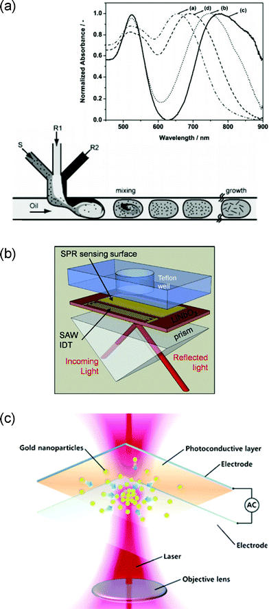 | ||
| Fig. 7 (a) A schematic diagram of droplet-based Au nano-rod synthesis. The inset shows that changes in the process parameters red-shifted the L-SPP resonance wavelength as far away as 750 nm. Reproduced with permission from ref. 123. (b) A schematically illustrated example of integrated SPR based on the combined utilization of microfluidic, plasmonic, and surface-acoustic functionalities. Reproduced from ref. 131. (c) An illustration of on-demand SERS hot-spot formation utilizing electrooptofluidic functional integration. Reproduced from ref. 137. | ||
7. Trends and outlooks
This survey, based on the level of dependence framework, revealed that the realization of critical-level integration, whether intended or not, has become increasingly frequent in plasmo-fluidics as the length-scale shrinks towards nanoscale. In particular, through a careful examination, one may find that the plasmo-fluidic setups for L-SPP, photothermal conversion, SERS, and trapping share many common, inseparable features, resulting in their simultaneous occurrences. We anticipate that the trend will accelerate its pace over the foreseeable future, getting benefits from the nanoscale tools currently under development. Light-driven nanoscale plasmonic motors129 and nano-antennas capable of regulating the flow of the SPP below the diffraction-limit130 constitute just an initial set of examples. Convergence-level integration of plasmo-fluidic functionalities will also continue. A few recently surfaced topics shed light on its future outlook.7.1 Incorporation of new functionalities
Currently the field of microfluidics is replete with newly introduced functionalities and architectures. Previously overlooked physical mechanisms are also finding their places in the lab-on-a-chip domain. All these will influence and enrich the field of plasmo-fluidics. One prominent example, droplet-based microfluidic functionalities and their integration with those of plasmonics, has already been discussed in Sections 2 and 6.3. A more recent development is the adoption of the surface acoustic wave (SAW). When combined with microfluidic channels, it can enhance the performance of micromixing through acousto-streaming and clarify molecular binding kinetics by shrugging off unwanted molecules nonspecifically bound to the surface. As shown in Fig. 7b, these beneficial effects have already been integrated with SPR.131 Interestingly, the integration of SAW and SPR has also been performed on a droplet-based platform.132 While improving the accuracy of kinetic parameter estimation was the original motivation for the work, the seamless integration of microfluidic, plasmonic, and acoustic functionalities is suggestive of future directions in the development of multi-functional biosensing platforms.7.2 Emphasis on on-demand reconfigurability
Another trend in plasmo-fluidic integration is the growing emphasis on dynamically reconfigurable functionalities. On-demand formation of SERS hot-spots and active pre-concentration of the analyte molecules represent recent developments. Optical trapping-based aggregation of metallic NPs has long been utilized to form SERS hot-spots on demand.133–135 Recently, the aggregation mechanism has been extended to include magnetic,136 electrooptofluidic137 (illustrated schematically in Fig. 7c), pneumatic soft-MEMS,138 and electro-osmotic/kinetic ones.139 A separate set of schemes, based on electric field gradient force36 or electro-kinetic force,140 have been developed for pre-concentration of analytes. It is anticipated that the two on-demand operations will be combined in near future, enabling an entirely dynamic control of microfluidic SERS. Some passive implementations have already appeared in nanofluidics settings.141–1447.3 Exploration of new plasmonic length-scales
While nanoscale plasmonic resonators in the form of particles, holes, or gaps have enabled sub-diffraction-limit, molecule-level sensing, they are often too complex and costly to achieve, especially for one-time use along with cheap, polymeric lab-on-a-chip devices. Between the nanoscale plasmonic resonators and sub-millimeter-scale integrated optic interferometers, whispering gallery mode (WGM) resonators exist as an alternative. The resonator's multi-micron length-scale is ideal for integration with microfluidic architectures. Their high-Q resonance leads to excellent sensitivity and low detection limit as well. However, the notoriously difficult coupling of light in and out of these WGM resonators has been huddling their wider adoption.Two approaches have been taken to address the issue. Amarie et al. utilized sub-micron-scale spherical metal cavities that are big enough for simple, sacrificial microsphere-based fabrication yet small enough to host plasmonic resonance modes.145,146 The second scheme utilized the Au NP as an optical antenna that catches the impinging excitation light and transfers it to the WGM-hosting microsphere. Simultaneous exploitation of the large extinction cross-section and strong evanescent field of an Au NP under plasmonic resonance for WGM excitation was the main motivation of this scheme. Since Au NPs are significantly smaller than the microsphere WGM resonator, they were raised to the height of the microsphere's equatorial plane by a set of dielectric rods fabricated with MEMS technology.147 It is anticipated that there will be more efforts to develop this type of MEMS-assisted, opto-plasmonically hybridized functionalities for use in microfluidics.
7.4 New read-out schemes
Recent development shows that the read-out schemes for plasmo-fluidic sensors need not be limited to optical ones. Electrical detection through an on-chip integrated photodiode has already been reported.148 Further simplification is expected along the path. One newly raised, yet important issue in the field of lab-on-a-chip is its suitability for use in developing countries where access to scientific/clinical facilities is severely limited.149,150 In such circumstances, the utility of nanoscale plasmo-fluidic schemes requiring spectroscopic apparatus for the retrieval of its diagnostic data will be limited. To cope with the issue, it may be best to seek solutions from nanotechnology itself. Recent work by Yanik et al., which utilized Fano resonance to visualize protein binding for naked-eye observation, provides useful insights in this respect.151 We anticipate that technologies capable of translating molecular-level events directly into visually observable optical signals, such as the one based on the morphological changes of nematic liquid crystal,152 will eventually prevail.Acknowledgements
This work was supported through National Science Foundation grants ECCS-1147413 and ECCS-0954845.References
- C. Monat, P. Domachuk, C. Grillet, M. Collins, B. J. Eggleton, M. Cronin-Golomb, S. Mutzenich, T. Mahmud, G. Rosengarten and A. Mitchell, Microfluid. Nanofluid., 2008, 4, 81–95 CrossRef.
- L. Pang, H. M. Chen, L. Wang, J. M. Beechem and Y. Fainman, Opt. Express, 2009, 17, 147000 Search PubMed.
- T. H. Seefeld, W. Zhou and R. M. Corn, Langmuir, 2011, 27, 6534–6540 CrossRef CAS.
- T. Springer, M. Piliarik and J. Homola, Sens. Actuators, B, 2010, 145, 588–591 CrossRef.
- S. Choi, S. Huang, J. Li and J. Chae, Lab Chip, 2011, 11, 3681 RSC.
- A. Hemmi, T. Usui, A. Moto, T. Tobita, N. Soh, K. Nakano, H. Zeng, K. Uchiyama, T. Imato and H. Nakajima, J. Sep. Sci., 2011, 34, 2913–2919 CrossRef CAS.
- M. Okan, O. Balci and C. Kocabas, Sens. Actuators, B, 2011, 160, 670–676 CrossRef CAS.
- T. Ghosh, L. Williams and C. H. Mastrangelo, Lab Chip, 2011, 11, 4194 RSC.
- Y. Luo, F. Yu and R. N. Zare, Lab Chip, 2008, 8, 694 RSC.
- K. Lee, Y. Su, S. Chen, F. Tseng and G. W. Lee, Biosens. Bioelectron., 2007, 23, 466–472 CrossRef CAS.
- G. Krishnamoorthy, E. T. Carlen, D. Kohlheyer, R. B. M. Schasfoort and A. van den Berg, Anal. Chem., 2008, 81, 1957–1963 CrossRef.
- E. Ouellet, C. Lausted, T. Lin, C. W. T. Yang, L. Hood and E. T. Lagally, Lab Chip, 2010, 10, 581–588 RSC.
- S. Natarajan, P. S. Katsamba, A. Miles, J. Eckman, G. A. Papalia, R. L. Rich, B. K. Gale and D. G. Myszka, Anal. Biochem., 2008, 373, 141–146 CrossRef CAS.
- J. Liu, M. A. Eddings, A. R. Miles, R. Bukasov, B. K. Gale and J. S. Shumaker-Perry, Anal. Chem., 2008, 81, 4296–4301 CrossRef.
- L. Malic, T. Veres and M. Tabrizian, Biosens. Bioelectron., 2011, 26, 2053–2059 CrossRef CAS.
- I. Kim and K. D. Kihm, Opt. Lett., 2010, 35, 393–395 CrossRef CAS.
- T. Gervais and K. F. Jensen, Chem. Eng. Sci., 2006, 61, 1102–1121 CrossRef CAS.
- T. M. Squires, R. J. Messinger and S. C. Manalis, Nat. Biotechnol., 2008, 26, 417–426 CrossRef CAS.
- K. J. Lee, M. J. Motala, M. A. Meitl, W. R. Childs, E. Menard, A. K. Shim, J. A. Rogers and R. G. Nuzzo, Adv. Mater., 2005, 17, 2332–2336 CrossRef CAS.
- H. Sipova, D. Vrba and J. Homola, Anal. Chem., 2012, 84, 30–33 CrossRef CAS.
- A. Prabhakar and S. Mukherji, Lab Chip, 2010, 10, 3422–3425 RSC.
- S. Y. Lee, S. Kim, S. G. Jang, C. Heo, J. W. Shim and S. Yang, Anal. Chem., 2011, 83, 9174–9180 CrossRef CAS.
- H. Gao, J. Yang, J. Y. Lin, A. D. Stuparu, M. H. Lee, M. Mrksich and T. W. Odom, Nano Lett., 2010, 10, 2549–2554 CrossRef CAS.
- K. Nakamoto, R. Kurita, O. Niwa, T. Fujii and M. Nishida, Nanoscale, 2011, 3, 5067–5075 RSC.
- L. Pang, G. M. Hwang, B. Slutsky and Y. Fainman, Appl. Phys. Lett., 2007, 91, 123112 CrossRef.
- H. Im, J. N. Sutherland, J. A. Manyard and S. Oh, Anal. Chem., 2012, 84, 1941–1947 CrossRef CAS.
- C. Escobedo, S. Vincent, A. I. K. Choudhury, J. Campbell, A. G. Brolo, D. Sinton and R. Gordon, J. Micromech. Microeng., 2011, 21, 115001 CrossRef.
- T. Chang, M. Huang, A. A. Yanik, H. Tsai, P. Shi, S. Aksu, M. F. Yanik and H. Altug, Lab Chip, 2011, 11, 3596 RSC.
- A. A. Yanik, M. Huang, O. Kamohara, A. Artar, T. W. Geisbert, J. H. Connor and H. Altug, Nano Lett., 2010, 10, 4962 CrossRef CAS.
- H. Im, N. J. Wittenberg, A. Lesuffleur, N. C. Lindquist and S. Oh, Chem. Sci., 2010, 1, 688–696 RSC.
- J. Ferreira, M. J. L. Santos, M. M. Rahman, A. G. Brolo, R. Gordon, D. Sinton and E. M. Girotto, J. Am. Chem. Soc., 2009, 131, 436–437 CrossRef CAS.
- F. Eftekahri, C. Escobedo, J. Ferreira, X. Duan, E. M. Girotto, A. G. Brolo, R. Gordon and D. Sinton, Anal. Chem., 2009, 81, 4308 CrossRef.
- C. Escobedo, A. G. Brolo, R. Gordon and D. Sinton, Anal. Chem., 2010, 82, 10015 CrossRef CAS.
- A. A. Yanik, M. Huang, A. Artar, T. Cheng and H. Altug, Appl. Phys. Lett., 2010, 96, 021101 CrossRef.
- M. P. Jonsson, A. B. Dahlin, L. Feuz, S. Petronis and F. Hook, Anal. Chem., 2010, 82, 2087 CrossRef CAS.
- C. Escobedo, A. G. Brolo, R. Gordon and D. Sinton, Nano Lett., 2012, 12, 1592 CrossRef CAS.
- J. J. Burke, G. I. Stegeman and T. Tamir, Phys. Rev. B, 1986, 33, 5186 CrossRef CAS.
- A. Degiron, P. Berini and D. R. Smith, Opt. Photonics News, 2008, 19, 29–34 CrossRef.
- P. Berini, R. Charbonneau and N. Lahoud, Nano Lett., 2007, 7, 1376 CrossRef CAS.
- C. Chiu, E. Lisicka-Skrzek, R. N. Tait and P. Berini, J. Vac. Sci. Technol., B: Microelectron. Nanometer Struct.–Process., Meas., Phenom., 2010, 28, 729 CrossRef CAS.
- C. Chiu, E. Lisicka-Skrzek, R. N. Tait and P. Berini, J. Vac. Sci. Technol., B: Microelectron. Nanometer Struct.–Process., Meas., Phenom., 2011, 29, 062601 CrossRef.
- A. W. Wark, H. J. Lee and R. M. Corn, Anal. Chem., 2005, 77, 3904 CrossRef CAS.
- R. Slavik and J. Homola, Sens. Actuators, B, 2007, 123, 10 CrossRef.
- A. Khan, O. Krupin, E. Lisicka-Skrzek and P. Berini, Proc. SPIE–Int. Soc. Opt. Eng., 2011, 8007, 800703 CrossRef.
- T. Kan, H. Kojo, E. Iwase, K. Matsumoto and I. Shimoyama, J. Micromech. Microeng., 2010, 20, 125005 CrossRef.
- V. N. Konopsky and E. V. Alieva, Opt. Lett., 2009, 34, 479 CrossRef CAS.
- V. N. Konopsky, D. V. Basmanov, E. V. Alieva, D. I. Dolgy, E. D. Olshansky, S. K. Sekatskii and G. Dietler, New J. Phys., 2009, 11, 063049 CrossRef.
- Y. H. Joo, S. H. Song and R. Magnusson, Appl. Phys. Lett., 2010, 97, 201105 CrossRef.
- H. H. Richardson, M. T. Carlson, P. J. Tandler, P. Hernandez and A. O. Govorov, Nano Lett., 2009, 9, 1139 CrossRef CAS.
- E. A. Coronado, E. R. Encina and F. D. Stefani, Nanoscale, 2011, 3, 4042 RSC.
- C. Loo, A. Lowery, N. J. Halas, J. West, R. Drezek and J. L. West, Nano Lett., 2005, 5, 709 CrossRef CAS.
- S. E. Lee, G. L. Liu, F. Kim and L. P. Lee, Nano Lett., 2009, 9, 562 CrossRef CAS.
- D. Boyer, P. Tamarat, A. Maali, B. Lounis and M. Orrit, Science, 2002, 297, 1160 CrossRef CAS.
- X. Miao, B. K. Wilson and L. Y. Lin, Appl. Phys. Lett., 2008, 92, 124108 CrossRef.
- K. H. Cheong, D. K. Yi, J. Lee, J. Park, M. J. Kim, J. B. Edel and C. Ko, Lab Chip, 2008, 8, 810 RSC.
- S. K. Kim, C. Heo, J. Y. Choi, S. Y. Lee, S. G. Jang, J. W. Shim, T. S. Seo and S. Yang, Appl. Phys. Lett., 2011, 98, 233701 CrossRef.
- M. Krishnan, J. Park and D. Erickson, Opt. Lett., 2009, 34, 1976 CrossRef.
- C. Fang, L. Shao, Y. Zhao, J. Wang and H. Wu, Adv. Mater., 2012, 24, 94 CrossRef CAS.
- M. Fedoruk, A. A. Lutich and J. Feldmann, ACS Nano, 2011, 5, 7377 CrossRef CAS.
- G. L. Liu, J. Kim, Y. Lu and L. P. Lee, Nat. Mater., 2006, 5, 27 CrossRef CAS.
- J. R. Adleman, D. A. Boyd, D. G. Goodwin and D. Psaltis, Nano Lett., 2009, 9, 4417 CrossRef CAS.
- P. Christopher, H. Xin and S. Linic, Natuer Chem., 2011, 3, 467 CAS.
- S. Linic, P. Christopher and D. B. Ingram, Nat. Mater., 2011, 10, 911 CrossRef CAS.
- L. Lei, N. Wang, X. M. Zhang, Q. Tai, D. P. Tsai and H. L. W. Chan, Biomicrofluidics, 2010, 4, 043004 CrossRef.
- R. S. Golightly, W. E. Doering and M. J. Natan, ACS Nano, 2009, 3, 2859 CrossRef CAS.
- Y. S. Huh, A. J. Chung and D. Erickson, Microfluid. Nanofluid., 2009, 6, 285 CrossRef CAS.
- C. Lim, J. Hong, B. G. Chung, A. J. deMello and J. Choo, Analyst, 2010, 135, 837 RSC.
- E. L. Izake, Forensic Sci. Int., 2010, 202, 1 CrossRef CAS.
- A. Marz, T. Henkel, D. Cialla, M. Schmitt and J. Popp, Lab Chip, 2011, 11, 3584 RSC.
- Y. Yin, T. Qiu, W. Zhang and P. K. Chu, J. Mater. Res., 2011, 26, 170 CrossRef CAS.
- M. Fan, G. F. S. Andrade and A. G. Brolo, Anal. Chim. Acta, 2011, 693, 7 CrossRef CAS.
- D. Cialla, A. Marz, R. Bohme, F. Theil, K. Weber, M. Schmitt and J. Popp, Anal. Bioanal. Chem., 2012, 403, 27 CrossRef CAS.
- L. Tong, K. Ramser and M. Kall, Raman spectroscopy for nanomaterials characterization, ed. C. S. S. R. Kumar, Springer, 2012 Search PubMed.
- R. A. Alvarez-Puebla and L. M. Liz-Marzan, Small, 2010, 6, 604 CrossRef CAS.
- I. M. White, S. H. Yazdi and W. W. Yu, Microfluidc. Nanofluid., 2012 DOI:10.1007/s10404-012-0962-2.
- V. Vlasko-Vlasov, A. Joshi-Imre, J. T. Bahns, L. Chen, L. Ocola and U. Welp, Appl. Phys. Lett., 2010, 96, 203103 CrossRef.
- M. Fan, P. Wang, C. Escobedo, D. Sinton and A. G. Brolo, Lab Chip, 2012, 12, 1554 RSC.
- C. L. Haynes and R. P. Van Duyne, J. Phys. Chem. B, 2003, 107, 7426 CrossRef CAS.
- X. Deng, G. B. Braun, S. Liu, P. F. Sciortino, B. Koefer, T. Tombler and M. Moskovits, Nano Lett., 2010, 10, 1780 CrossRef CAS.
- A. Kocabas, G. Ertas, S. S. Senlik and A. Aydinli, Opt. Express, 2008, 16, 12469 CrossRef CAS.
- J. Li, D. Fattal and Z. Li, Appl. Phys. Lett., 2009, 94, 263114 CrossRef.
- M. Hu, D. Fattal, J. Li, X. Li, Z. Li and R. S. Williams, Appl. Phys. A: Mater. Sci. Process., 2011, 105, 261 CrossRef CAS.
- J. Xu, P. Guan, P. Kvasnicka, H. Gong, J. Homola and Q. Yu, J. Phys. Chem. A, 2011, 115, 10996 CrossRef CAS.
- R. B. Schoch, J. Han and P. Renaud, Rev. Mod. Phys., 2008, 80, 839–883 CrossRef CAS.
- Y. J. Oh, S. Park, M. Kang, J. Choi, Y. Nam and K. H. Jeong, Small, 2011, 7, 184 CrossRef CAS.
- C. Andreou, M. R. Hoonejani, M. R. Barmi, B. Piorek, M. Moskovits and C. D. Meinhart, MicroTAS, 2011, 1671 Search PubMed.
- A. Louvera and O. J. F. Martin, Proc. SPIE, 2011, 8097, 1Q Search PubMed.
- M. L. Juan, M. Righini and R. Quidant, Nat. Photonics, 2011, 5, 349 CrossRef CAS.
- D. Erickson, X. Serey, Y. Chen and S. Mandal, Lab Chip, 2011, 11, 995 RSC.
- X. Miao and L. Y. Lin, IEEE J. Sel. Top. Quantum Electron., 2007, 13, 1655 CrossRef CAS.
- D. Li, Y. Xi and H. K. Kim, J. Appl. Phys., 2011, 110, 103108 CrossRef.
- K. Wang, E. Schonbrun, P. Steinvurzel and K. B. Crozier, Nano Lett., 2010, 10, 3506 CrossRef CAS.
- M. Juan, R. Gordon, Y. Pang, F. Eftekhari and R. Quidant, Nat. Phys., 2009, 5, 915 CrossRef CAS.
- C. Chen, M. L. Juan, Y. Li, G. Maes, G. Borghs, P. Van Dorpe and R. Quidant, Nano Lett., 2012, 12, 125 CrossRef CAS.
- A. Ohlinger, S. Nedev, A. A. Lutich and J. Feldmann, Nano Lett., 2011, 11, 1770 CrossRef CAS.
- J. S. Donner, G. Baffou, D. McCloskey and R. Quidant, ACS Nano, 2011, 5, 5457 CrossRef CAS.
- W. Zhang, L. Huang, C. Santschi and O. J. F. Martin, Nano Lett., 2010, 10, 1006 CrossRef CAS.
- B. J. Roxworthy, K. D. Ko, A. Kumar, K. H. Fung, E. K. C. Chow, G. L. Liu, N. X. Fang and K. C. Toussaint, Nano Lett., 2012, 12, 796 CrossRef CAS.
- B. J. Roxworthy and K. C. Toussaint, Opt. Express, 2012, 20, 9591 CrossRef CAS.
- Y. Song, J. Hormes and C. S. S. R. Kumar, Small, 2008, 4, 698 CrossRef CAS.
- J. Wagner, T. Kirner, G. Mayer, J. Albert and J. M. Kohler, Chem. Eng. J., 2004, 101, 251 CrossRef CAS.
- D. Shalom, R. C. R. Wootton, R. F. Winkle, B. F. Cottam, R. Vilar, A. J. deMello and C. P. Wilde, Mater. Lett., 2007, 61, 1146 CrossRef CAS.
- C. Wu and T. Zeng, Chem. Mater., 2007, 19, 123 CrossRef CAS.
- S. T. He, Y. L. Liu and H. Maeda, J. Nanopart. Res., 2008, 10, 209 CrossRef CAS.
- A. Singh, M. Shirolkar, N. P. Lalla, C. K. Malek and S. K. Kulkarni, Int. J. Nanotechnol., 2009, 6, 541 CrossRef CAS.
- Z. Chang, C. A. Serra, M. Bouquey, I. Kraus, S. Li and J. M. Kohler, Nanotechnology, 2010, 21, 015605 CrossRef.
- D. V. R. Kumar, M. Kasture, A. A. Prabhune, C. V. Ramana, B. L. V. Prasad and A. A. Kulkarni, Green Chem., 2010, 12, 609 RSC.
- F. Jamal, G. Jean-Sebastien, P. Mael, P. Edmond and R. Christian, Microsyst. Technol., 2012, 18, 151 CrossRef CAS.
- A. Vogel and V. Venugopalan, Chem. Rev., 2003, 103, 577 CrossRef CAS.
- B. D. Chithrani, A. A. Ghazani and W. C. W. Chan, Nano Lett., 2006, 6, 662 CrossRef CAS.
- J. M. Kohler, J. Wagner and J. Albert, J. Mater. Chem., 2005, 15, 1924 RSC.
- J. M. Kohler, H. Romanus, U. Hubner and J. Wagner, J. Nanomater., 2007, 98134 Search PubMed.
- J. M. Kohler, M. Held, U. Hubner and J. Wagner, Chem. Eng. Technol., 2007, 30, 347 CrossRef.
- J. M. Kohler, L. Abahmane, J. Wagner, J. Albert and G. Mayer, Chem. Eng. Sci., 2008, 63, 5048 CrossRef.
- J. Wagner, T. R. Tshikhudo and J. M. Kohler, Chem. Eng. J., 2008, 135S, S104 CrossRef.
- H. Tsunoyama, N. Ichikuni and T. Tsukuda, Langmuir, 2008, 24, 11327 CrossRef CAS.
- K. Sugano, Y. Uchida, O. Ichihashi, H. Yamada, T. Tsuchiya and O. Tabata, Microfluid. Nanofluid., 2010, 9, 1165 CrossRef CAS.
- C. Weng, C. Huang, C. Yeh, H. Lei and G. B. Lee, J. Micromech. Microeng., 2008, 18, 035019 CrossRef.
- S. Yang, F. Cheng, C. Yeh and G. B. Lee, Microfluid. Nanofluid., 2010, 8, 303 CrossRef CAS.
- S. Gomez-de Pedro, M. Puyol and J. Alonso-Chamarro, Nanotechnology, 2010, 21, 415603 CrossRef CAS.
- S. A. Khan and K. F. Jensen, Adv. Mater., 2007, 19, 2556 CrossRef CAS.
- J. I. Park, A. Saffari, S. Kumar, A. Gunther and E. Kumacheva, Ann. Rev. Mater. Res., 2010, 40, 415–443 CrossRef CAS.
- S. Duraiswamy and S. A. Khan, Small, 2009, 5, 2828 CrossRef CAS.
- L. L. Lazarus, A. S. J. Yang, S. Chu, R. L. Brutchey and N. Malmstadt, Lab Chip, 2010, 10, 3377 RSC.
- S. Duraiswamy and S. A. Khan, Nano Lett., 2010, 10, 3757 CrossRef CAS.
- A. Knauer, A. Thete, S. Li, H. Romanus, A. Csaki, W. Fritzsche and J. M. Kohler, Chem. Eng. J., 2011, 166, 1164 CrossRef CAS.
- G. Laurent, N. Felidj, J. Aubard and G. Levi, Phys. Rev. B: Condens. Matter Mater. Phys., 2005, 71, 045430 CrossRef.
- E. Prodan, C. Radloff, N. J. Halas and P. Nordlander, Science, 2003, 302, 419 CrossRef CAS.
- M. Liu, T. Zentgraf, Y. Liu, G. Bartal and X. Zhang, Nat. Nanotechnol., 2010, 5, 570 CrossRef CAS.
- J. Kang, K. Kim, H. Ee, Y. Lee, T. Yoon, M. Seo and H. Park, Nat. Commun., 2011, 2, 582 CrossRef.
- A. Renaudin, V. Chabot, E. Grondin, V. Aimez and P. G. Charett, Lab Chip, 2010, 10, 111 RSC.
- E. Galopin, M. Beaugeois, B. Pinchemel, J. Camart, M. Bouazaoui and V. Thomy, Biosens. Bioelectron., 2007, 23, 746 CrossRef CAS.
- H. Yoshikawa, T. Matsui and H. Masuhara, Phys. Rev. E: Stat., Nonlinear, Soft Matter Phys., 2004, 70, 061406 CrossRef.
- Y. Tanaka, H. Yoshikawa, T. Itoh and M. Ishikawa, J. Phys. Chem. C, 2009, 113, 11856 CAS.
- L. Tong, M. Righini, M. U. Gonzalez, R. Quidant and M. Kall, Lab Chip, 2009, 9, 193 RSC.
- B. Han, N. Choi, K. H. Kim, D. W. Lim and J. Choo, J. Phys. Chem. C, 2011, 115, 6290 CAS.
- H. Hwang, D. Han, Y. Oh, Y. Cho, K. H. Jeong and J. Park, Lab Chip, 2011, 11, 2518 RSC.
- J. Zhou, K. Ren, Y. Zhao, W. Dai and H. Wu, Anal. Bioanal. Chem., 2012, 402, 1601 CrossRef CAS.
- K. B. Kim, J. Han, H. Choi, H. C. Kim and T. D. Chung, Small, 2012, 8, 378 CrossRef CAS.
- H. Cho, B. Lee, G. L. Liu, A. Agarwal and L. P. Lee, Lab Chip, 2009, 9, 3360 RSC.
- M. Wang, M. Benford, N. Jing, G. Cote and J. Kameoka, Microfluid. Nanofluid., 2009, 6, 411 CrossRef CAS.
- S. H. Yadzi and I. M. White, Biomicrofluidics, 2012, 6, 014105 CrossRef.
- I. Choi, Y. S. Huh and D. Erickson, Lab Chip, 2011, 11, 632 RSC.
- L. C. Taylor, T. B. Kirchner, N. V. Lavrik and M. J. Sepaniak, Analyst, 2012, 137, 1005 RSC.
- D. Amarie, T. Onuta, R. A. Potyrailo and B. Dragnea, J. Phys. Chem. B, 2005, 109, 15515 CrossRef CAS.
- D. Amarie, A. Alileche, B. Dragnea and J. A. Glazier, Anal. Chem., 2010, 82, 343 CrossRef CAS.
- W. Ahn, S. V. Boriskina, Y. Hong and B. M. Reinhardt, ACS Nano, 2012, 6, 951 CrossRef CAS.
- F. Mazzotta, G. Wang, C. Hagglund, F. Hook and M. P. Jonsson, Biosens. Bioelectron., 2010, 26, 1131 CrossRef CAS.
- W. G. Lee, Y. Kim, B. G. Cheung, U. Demirci and A. Khademhosseini, Adv. Drug Delivery Rev., 2010, 62, 449–457 CrossRef CAS.
- X. Mao and T. J. Huang, Lab Chip, 2012, 12, 1412 RSC.
- A. A. Yanik, A. E. Cetin, M. Huang, A. Artar, S. H. Mousavic, A. Khanikaevc, J. H. Connord, G. Shvetsc and H. Altug, Proc. Natl. Acad. Sci. U. S. A., 2011, 108, 11784 CrossRef CAS.
- K. D. Cadwell, N. A. Lockwood, B. A. Nellis, M. E. Alf, C. R. Willis and N. L. Abbott, Sens. Actuators, B, 2007, 128, 91–98 CrossRef.
Footnote |
| † Published as part of a themed issue on optofluidics. |
| This journal is © The Royal Society of Chemistry 2012 |