Metal sulfide nanostructures: synthesis, properties and applications in energy conversion and storage
Chen-Ho
Lai
,
Ming-Yen
Lu
and
Lih-Juann
Chen
*
Department of Materials Science and Engineering, National Tsing Hua University, Hsinchu, Taiwan, Republic of China. E-mail: ljchen@mx.nthu.edu.tw; Fax: +886-3-5718328; Tel: +886-3-5731166
First published on 10th November 2011
Abstract
Metal sulfide nanomaterials have attracted great attention because of their excellent properties and promising applications in electronic, optical and optoelectronic devices. Well-aligned nanostructure arrays on substrates are highly attractive for their enhanced properties and novel applications. The general solution route and thermal evaporation under controlled conditions have been utilized for oriented growth of various metal sulfide nanostructure arrays and demonstrated their applications in energy conversion and storage. The article provides an overview of recent research and significant advances reported in the literature, covering from synthesis to properties and to applications especially in energy conversion and storage, such as lithium-ion batteries, solar cells, fuel cells and piezoelectric nanogenerators.
 Chen-Ho Lai | Chen-Ho Lai received his BS in Mechanical Engineering from National Central University in 2005 and his PhD in Materials Science and Engineering from National Tsing Hua University in 2011 under the supervision of Prof. Lih-Juann Chen. His research interests include the controlled synthesis and characterization of various metal chalcogenide nanostructures with novel applications in electronics, optoelectronics, and energy conversion and storage devices. |
 Ming-Yen Lu | Ming-Yen Lu studied Materials Science and Engineering at National Tsing Hua University in Taiwan where he also received his PhD degree in 2009 working on synthesis and applications of ZnS-based nanostructures under the supervision of Prof. L. J. Chen. He is currently a postdoctoral fellow with Prof. L. J. Chen and Prof. S. Gwo (physics, National Tsing Hua University, Taiwan). His research interests include flexible electronic nanodevices, in situ TEM observations for dynamic study on solid state and liquid reactions, and III-Nitride nanostructures for solid state lighting. |
 Lih-Juann Chen | Lih J. Chen is the President of National Tsing Hua University (NTHU), Taiwan. He received PhD degree in physics from University of California, Berkeley in 1974 and is currently National Chair Professor at the Department of Materials Science and Engineering, NTHU. His main interests in research are synthesis and applications of low-dimensional nanomaterials, atomic scale structures and dynamic processes of advanced materials as well as metallization in integrated circuit devices. |
Introduction
Nanostructured materials have attracted great interest due to their electrical, optical, magnetic and mechanical properties contributed by confining the dimensions of such materials, and the entire behaviors of nanostructured materials show combinations of surface and bulk properties.1–4 Low-dimensional nanostructured materials have been successfully synthesized and have drawn much attention because of their fundamental roles in understanding the quantum size effect and great potential applications in light-emitting diodes, gas sensors, nanothermometers, solar cells, fuel cells, piezoelectric nanogenerators and lithium-ion batteries.5,6 One-dimensional (1D) nanostructures are ideal for investigating the dependence of electrical transport, optical and mechanical properties on size and dimensionality. Well-aligned one-dimensional nanostructures on substrates are highly attractive for device applications in particular. They are expected to play key roles as both interconnects and functional components in developing new generation nanodevices with high performance.7,8 Many unique and excellent properties have already been proposed or demonstrated in recent years, such as lower turn-on voltage for field emitters, superior mechanical toughness, higher efficiency for solar cells, enhancement of thermoelectric figure of merit and better electrochemical performance for lithium-ion batteries.9,10 Two-dimensional (2D) nanostructures, such as nanoplates, nanosheets and nanowalls, are suggested to be ideal components for nanoscale devices used in biological sensors, nanoswitches and data storage due to their high surface-to-volume ratio, nanometre-scale thickness and fascinating optical and photocatalytic activities.11One of the great challenges in the 21st century is undoubtedly energy conversion and storage. The present energy-conscious society calls for light-weight, low-cost, high-efficiency and environmentally friendly renewable energies due to the increasing demand for oil and environmental issues.12 Much important progress has been made in the development of advanced energy conversion and storage technologies such as solar cells, biofuels, piezoelectric nanogenerators, fuel cells and lithium-ion batteries. A variety of new alternative energy conversion and storage technologies have been developed and made renewable energies more competitive with fossil fuels, but they have not been in widespread use due to limitation of the materials properties. Further improvements are needed to satisfy the great challenges for today's information and mobile society.13 Novel nanostructured materials provide great opportunities to improve performance of these renewable energy conversion and storage technologies due to their unique characteristics. Nanostructured materials are potential materials for renewable energy conversion and storage. Advantages include (i) improving cycle life with better flexibility, (ii) providing additional reactive sites and catalytic activity, (iii) improved conductivity of the developed composite nanostructured materials resulting in the decrease of inner resistance and Ohmic loss, and (iv) short path lengths for transport of electrons.14,15
Nanostructured metal sulfides have been extensively studied due to their importance in interpreting quantum size effects and applications in a variety of devices, such as solar cells, light-emitting diodes, sensors, thermoelectric devices, lithium-ion batteries, fuel cells and nonvolatile memory devices.16–18 Metal sulfides are a major group of minerals that provide the crystal chemist a rich field for investigation due to their diverse structural types. They are abundant and cheap since they usually exist in nature as minerals such as heazlewoodite (Ni3S2), chalcocite (Cu2S), pyrite (FeS2) and so on. We have synthesized various metal sulfide nanostructure arrays, such as ZnS, Cu2S, Ni3S2 and Co9S8. Zinc sulfide (ZnS) is an important II–VI semiconducting material with a wide bandgap energy of 3.7 eV and a large exciton energy (∼40 meV). ZnS nanostructures have versatile potential applications as optoelectronic devices due to their excellent properties of luminescence and photochemistry, e.g., flat-panel displays, injection lasers and light-emitting diodes.19,20 On the other hand, ZnS can also serve as an important semiconductor photocatalyst to remove toxic or organic water pollutants owing to the highly negative reduction potentials of excited electrons and the rapid generation of electron–hole pairs.11Copper sulfide (Cu2S) is an important p-type semiconductor and has great potential applications as cathode materials for lithium-ion batteries, solar radiation absorbers and nonlinear optical materials.7 It is appealing as an extremely thin absorber layer in solar cells due to its nearly ideal bandgap of 1.2 eV and low cost. Cu2S can also be used as nanoscale switches because it is a mixed Cu ionic/electronic conductor.21,22 Transition metal sulfides such as cobalt sulfide (Co9S8) and nickel sulfide (Ni3S2) are very important hydrodesulfurization (HDS) catalysts because they are stable under severe sulfo-reductive conditions in hydroprocessing of petroleum-based feedstocks. Nickel sulfides are very interesting materials because of their potential as a transformation toughening agent for materials used in the semiconductor industry, coating for photogalvanic cells, hydrogen storage, cathode materials for lithium-ion batteries, anode materials for solid oxide fuel cells, selective hydrogenation of chloronitrobenzene and electrocatalysts for cathodic H2 evolution in water electrolysis.23,24 Single crystalline Ni3S2 is a good metallic conductor with a room temperature resistivity of about 1.8 × 10⁻⁵ Ω cm leading to ease in transportation for lithium ions and electrons. The magnetic susceptibility of Ni3S2 was found to be temperature independent, which is consistent with Pauli paramagnetism.25 The electronic and magnetic properties of Ni3S2 have attracted more interest which can be ascribed to strong electron–electron correlation, insulating ground state and magnetic instabilities. Recently, Ni3S2 has also been recognized to have high lithium activity and storage capacity for fabricating the cathode material of rechargeable lithium-ion batteries.26,27Co9S8 has attracted much attention because of its promising uses as anode materials for solid oxide fuel cells (SOFCs), rechargeable lithium-ion batteries and supercapacitors. Co9S8 was found to have the highest catalytic activity for dioxygen reduction in acidic solution among a variety of transition metal sulfides. Magnetic susceptibility measurement result revealed that Co9S8 is also of Pauli paramagnetism and can be used for fabricating the magnetic devices.28 Metallic property of Co9S8 may also promise potential application as interconnector and electrode material for lithium-ion batteries.29
Herein we present an overview and discuss future promising areas of metal sulfide nanostructures, covering from synthesis to properties and to applications in energy conversion and storage. We will focus on the electronic, optoelectronic, magnetic, piezoelectric and electrochemical devices based on potential applications of oriented metal sulfide nanostructures including lithium-ion batteries, fuel cells, solar cells and piezoelectric nanogenerators. Furthermore, the future outlook is addressed.
Synthesis
Metal sulfide nanostructures have been synthesized by a variety of chemical or physical methods. Among these are solution-phase reactions,16 hydrothermal growth,22 high-pressure autoclave processes,23,31physical vapor deposition (PVD)19,20 and chemical vapor deposition (CVD).30 Deposition-based synthesis methods are the most popular among these methods. Thermal evaporation methods (PVD and CVD), arc discharge, and laser-assisted growth are members of this group. The most common deposition-based synthesis methods are PVD and CVD.19 These methods consist of the physical transport of the vapor species to the site. In order to grow metal sulfide nanostructures at lower temperature and without using catalysts, high-pressure autoclave processes are commonly used to overcome the high interfacial energy between substrate, liquid and particle for oriented growth of metal sulfide nanostructures.23,31 There has been an increased emphasis on the topic of “green” chemistry and chemical processes. Environmentally benign reducing agents and nontoxic solvent media are some of the key issues that merit significant consideration in a green synthetic strategy. As life's basic building blocks, biomolecules have special structures and fascinating self-assembling functions, which make them an appropriate medium for the design and synthesis of nanostructures. Recently, biomolecule-assisted synthesis routes have been a new and promising focus in the production of various kinds of metal sulfide nanomaterials.32 Besides the reductive properties of biomolecules, they also have strong shape or size directing functionality in the reaction process.33a Although great progress has been achieved on the synthesis approach, most growth methods usually require high temperature, a series of complicated procedures, expensive equipment, surfactants, catalysts or templates which will increase the cost, contamination and energy-consumption. Therefore, searching for a simple, efficient, low cost, and environmentally benign approach for the high-yield production of one-dimensional metal chalcogenide nanomaterials is necessary.General solution route
We have developed a facile solution method for the oriented growth of large-scale metal sulfide nanostructure arrays.7,27 The preparation strategy combines metal chelation chemistry and dioxygen catalytic reactions. Interactions between molecules and metal surfaces can result in energy exchange with the electrons of the metal.33b The coordination of ethylenediamine–chalcogen solutions and hydrazine in alkali solution has been proved to have great advantages for the fabrication of metal sulfides with fewer instrumental limitations. This method is reliable and operates under mild template-free conditions for single-crystalline metal sulfide nanostructures production without using high-pressure autoclave processes. Fig. 1 shows a series of oriented metal sulfide nanostructures grown by our method on corresponding metal substrates indicating the generality of this route.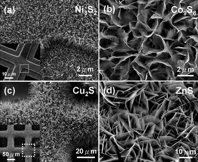 | ||
| Fig. 1 SEM images of a series of oriented metal sulfide nanostructures grown by a general solution route on corresponding metal substrates to demonstrate the generality of this route: (a) Ni3S2, (b) Co9S8, (c) Cu2S and (d) ZnS nanostructures.27 | ||
Thermal evaporation
As shown in Fig. 2, various zinc sulfide nanostructures, such as ZnS nanowire arrays, ZnO–ZnS heterojunction nanowire arrays, ZnS:Ga nanowalls and CoxZn1−xS nanowires, have been synthesized by thermal evaporation in a vacuum tube furnace under controlled conditions.11,34,35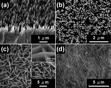 | ||
| Fig. 2 SEM images of various zinc sulfide nanostructures grown by the thermal evaporation method: (a) ZnS NW arrays, (b) ZnO–ZnS heterojunction NW arrays, (c) intercrossed sheet-like Ga-doped ZnS nanostructures and (d) CoxZn1−xS nanowires.11,34,35 | ||
One-dimensional single-crystalline DMS CoxZn1−xS nanowires with different doping levels have been synthesized by the thermal evaporation method using different amounts of CoCl2·6H2O powders as dopant source via the vapor–liquid–solid (VLS) growth mechanism.34 Axial heterostructured ZnO–ZnS NW arrays have been synthesized based on a one-step thermal evaporation with ZnS powders. Further, ZnS NW arrays can be obtained by etching the ZnO top portion away with KOH solution.35 Intercrossed sheet-like ZnS nanostructures with Ga dopant (ZnS:Ga nanowalls) have been grown on Si substrates by thermal evaporation of mixed powders of ZnS and Ga2O3via a self-catalyzed growth mechanism.11
Properties
Optical properties
Some of the metallic sulfides in the natural mineral state have very interesting optical properties. The spectral reflectivities, indices of refraction, and extinction indices of Sb2S3, MoS2, PbS, and FeS2 have been widely studied.36a Wide-band semiconducting metal sulfide nanostructures are good electrically driven lasing material and active optical waveguide material, which may find extensive applications in near-field optical lithography and telecommunications. One-dimensional nanostructured ZnS and CdS have received great attention for various optoelectronic applications, such as waveguides, field-effect transistors, lasers, solar cells, photodetectors, thin film electroluminescent displays and light emitting diodes.36b,c It is very important to fabricate nanomaterials with continuous tunable physical properties. II–VI group materials in the form of superlattices, heterostructures and quantum dots have been utilized for band gap engineering. To date, major problems continue to hamper the development of II–VI group materials for optoelectronic applications. First, the presence of defects which are derived from the polytypism of II–VI semiconducting materials. Second, the lack of reproducible doping to achieve desired electrical conductivity. Finally, the lack of high quality bulk single-crystalline II–VI semiconducting materials used as substrates.37,38 The “bottom-up” approach of utilizing nanomaterials may help to overcome these major problems. Recent investigations show that band gap tuning in II–VI semiconducting nanomaterials via controlling the constituent stoichiometry is more effective and efficient. Advances in ternary metal sulfide semiconductor nanostructures, such as ZnxCd1−xS nanoribbons, CdSxSe1−x nanobelts and ZnSexS1−x nanoarchitectures, have shown that their energy gaps and optical emissions can be tuned continuously by changing their constituent stoichiometry, dimensionality and size.37–39 The relationships between the constituent stoichiometry and lattice constants, and that between the chemical composition and band gap energy are systematically studied. These works show the feasibility of wavelength-controlled lasing in 1D ternary metal sulfide semiconductor nanostructures, covering the whole visible spectral range and may find significant applications in the tunable photoelectric nanodevices in the visible region.Recently, the studies of ZnO–ZnS heterostructures with various morphologies have been reported.40–42a These results demonstrate the feasibility of synthesizing high-quality crystalline heterostructure at the nanoscale level from two materials with a large lattice mismatch, which are otherwise difficult in bulk materials. At the nanoscale level, surface effects and small-size interface can exert considerable influence on the formation of high-quality heterojunctions free of dislocations in nanosized domains. However, the synthesis of ZnO–ZnS heterojunction NW arrays remains a challenge. We have successfully synthesized for the first time axial heterostructure ZnO–ZnS NW arrays based on a one-step thermal evaporation.35 Room-temperature cathodoluminescence (CL) spectra of the ZnO–ZnS NW arrays and ZnS NW arrays are shown in Fig. 3. The CL peaks for the ZnO–ZnS NW arrays and ZnS NW arrays are centered at 509 and 549 nm, respectively. The luminescence of ZnS at 509 nm was proposed to be due to the presence of Cu or Au impurities in the literature.42b Thus the blue-green emission may result from the Au employed in our synthesis. The luminescence from ZnO–ZnS NW arrays is located in the green region with its maximum intensity centered at 549 nm. Multipeak Gaussian fitting gives two Gaussian bands due to the asymmetric shape of the peak, and the Gaussian curve fits well with the experimental curve as shown in Fig. 3b. The blue-green peak supposedly results from ZnS as we discussed above. The other peak located at 557 nm is contributed from ZnO, and the emission arises from the recombination between electrons trapped at the oxygen vacancy and holes trapped at the surface defects.42c The SEM image and the corresponding CL image of ZnO/ZnS NW arrays are shown in the inset of Fig. 3b. The bright area of the CL image reveals the luminescent positions, and the main light-emitting locations are consistent with the positions of NW arrays. The findings point to versatile applications in the tunable optoelectronic nanodevices in the visible region. These special kinds of component-modulated nanomaterials not only offer the benefit of designing and producing nanoscale devices without further assembling, but also provide novel desirable properties.
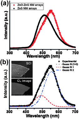 | ||
| Fig. 3 (a) Room-temperature CL spectra of ZnO–ZnS NW arrays. (b) Multipeak Gaussian fitting of the received CL spectra. Blue-green and green emissions are contributed from ZnS and ZnO, respectively. The inset shows the SEM image and the corresponding CL image of ZnO–ZnS NW arrays.35 | ||
Magnetic properties
Among the various metal sulfide nanomaterials we have synthesized, the transition-metal sulfides are an interesting group for magnetic studies due to the fact that electrons are in the partially filled d subshells. The magnetic susceptibility measurement results of various phases of cobalt sulfides revealed that CoS, Co3S4, and Co4S3 exhibit temperature-independent paramagnetism. CoS2 is ferromagnetic with a Curie temperature of 116 K and Co9S8 is antiferromagnetic with a Néel temperature above the decomposition temperature.28 The magnetic susceptibility of Ni3S2 was found to be temperature-independent, which is consistent with Pauli paramagnetism. There exist various types of iron sulfides with different Fe![[thin space (1/6-em)]](https://www.rsc.org/images/entities/char_2009.gif) :S ratios in nature.43a In general, iron sulfides present interesting magnetic properties which are related to the stoichiometric ratio between Fe and S as well as their crystalline structures. Among natural iron sulfide minerals, marcasite and pyrite are diamagnetic; greigite and pyrrhotite are ferrimagnetic; troilite is antiferromagnetic, and mackinawite is paramagnetic. Magnetic measurements showed that Fe7S8 and Fe9S8 nanostructures are ferromagnetic materials, showing magnetic hysteresis loops at room temperature.43b
:S ratios in nature.43a In general, iron sulfides present interesting magnetic properties which are related to the stoichiometric ratio between Fe and S as well as their crystalline structures. Among natural iron sulfide minerals, marcasite and pyrite are diamagnetic; greigite and pyrrhotite are ferrimagnetic; troilite is antiferromagnetic, and mackinawite is paramagnetic. Magnetic measurements showed that Fe7S8 and Fe9S8 nanostructures are ferromagnetic materials, showing magnetic hysteresis loops at room temperature.43b
The intrinsic properties of semiconductors can be permanently modified by introducing impurities as dopants. Semiconductors doped with transition metals may possess magnetic properties due to the partially filled d or f valence electron states of transition metals. In accordance with their spin, partially filled d or f valence electron states contain unpaired electrons that may exhibit a magnetic phenomenon. Substitutional doping of semiconductors with paramagnetic transitional-metal ions can produce materials called dilute magnetic semiconductors (DMSs).44 The interesting magneto-optical and magnetic properties of DMSs are spin-exchange interactions between the semiconductor charge carriers and the dopant ions.45 Great efforts have been devoted to the research of DMSs due to their promising applications in nanoscale spintronic devices, such as spin light-emitting diodes, nonvolatile memory and spin-valve transistors.46 One-dimensional single-crystalline DMS CoxZn1−xS nanowires with different doping levels have been synthesized by the thermal evaporation method.34 An example is shown in Fig. 4. Fig. 4a shows the hysteresis loop of the magnetization as a function of the applied magnetic field of CoxZn1−xS nanowires with different Co contents at 5 K, showing that the CoxZn1−xS nanowires are magnetic. The loops of CoxZn1−xS nanowires with low Co content show weak magnetization. The magnetism of the CoxZn1−xS nanowires is maintained at room temperature, and the saturated magnetization dramatically increases with the Co content in ZnS. Fig. 4b shows the hysteresis loops of CoxZn1−xS nanowires with 5.16% Co at 4, 40, and 300 K. The saturation magnetizations at 4, 40, and 400 K are 1.7 × 10⁻⁴, 1.49 × 10⁻⁴, and 7.45 × 10⁻⁵ emu, respectively. The magnetization of CoxZn1−xS nanowires may arise from the magnetic exchange interaction between Co ions. The result indicates that DMS CoxZn1−xS nanowires are expected to open up a number of opportunities for fundamental studies and ensure their promising applications for nanoscale spintronic devices.
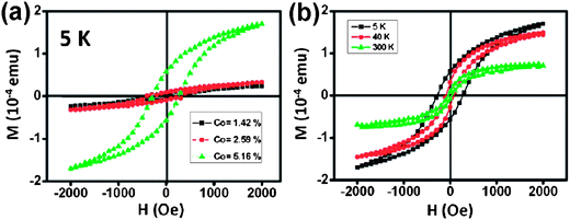 | ||
| Fig. 4 (a) M–H curves of CoxZn1−xS nanowires with different Co contents at 5 K. (b) M–H curves of CoxZn1−xS nanowires with 5.16% Co content at different temperatures.34 | ||
Electrical properties
Many metal sulfides, such as Co9S8 and Ni3S2, are good metallic conductors whereas magnetic instabilities and electronic interactions rendered them to be of marginal importance.25,28 They have attracted much attention because of their promising uses as cathode materials for rechargeable lithium-ion batteries, interconnectors, supercapacitors and anode materials for solid oxide fuel cells (SOFCs).26,27,29,47 Cu2S is a p-type semiconducting material with a bulk bandgap of 1.2 eV and can be potentially used as nanoswitches due to its mixed Cu ionic/electronic conductivity.21 ZnS is a II–VI semiconducting material with a wide bandgap energy of 3.7 eV.48Doping is an effective approach to tune the electrical properties of semiconductors and it has been widely used in the semiconductor industry. We successfully synthesized Co-doped ZnS nanowires by using a chemical vapor transport method. The metal chloride plays a critical role in the substitution of Zn with dopants. We demonstrate that the electrical properties of Co-doped ZnS nanowires can be tuned by introducing different doping levels.34Fig. 5 reveals the concentration dependence of conductivity in CoxZn1−xS nanowires. The conductivity of nanowires is tuned by introducing different amounts of dopants.49 In most cases of semiconductors, the increase in doping concentration leads to the increase in conductivity because of excess free carriers. The 3d-transition metals have higher solubility (10–25%) in II–VI compound semiconductors than that in III–V compound semiconductors.50 These results show that the Co-doped ZnS nanowires can be further utilized in practical device applications, such as magnetic and optical nanodevices.
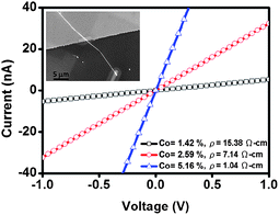 | ||
| Fig. 5 Room temperature I–V measurements of CoxZn1−xS nanowires with different Co contents (black: Co = 1.42%, ρ = 15.38 Ω cm; red: Co = 2.59%, ρ = 7.14 Ω cm; blue: Co = 5.16%, ρ = 1.04 Ω cm). The inset shows the SEM image of the nanowire device.34 | ||
Field-emission properties
Field-emission (FE) is one of the main characteristics of nanomaterials and nanostructures, and is of great commercial interest in displays. As compared with conventional technologies, nanostructures have many advantages such as faster device turn-on time, sustainability and compactness.51 Recent progress in the research on FE and stimulated emission properties of 1D wide band-gap semiconducting metal sulfide nanostructures has resulted in an important increase in the current density and decrease in the turn-on voltage. It has become forefront research due to growing demands of nanotechnologies and great commercial interest in flat panel displays. Effects of structural parameter, morphology and heterostructures on FE properties of semiconducting metal sulfide nanostructure arrays have been widely studied.52,53 Various metal sulfide semiconductor nanostructures with tailored geometries are ideal systems for investigating the dimensionality and size dependence of their properties for potential applications in displays.54,55Photocatalytic activity
Semiconductor nanomaterials for photocatalytic degradation of organic contaminants are promising materials in environmental protection nanotechnology. Titanium dioxide is an excellent photocatalyst because of its low cost, high stability and environmental friendliness. TiO2 has photoactivity only under ultraviolet light irradiation, which is the major drawback owing to its large band gap energy of 3.2 eV. The development of new visible light-active photocatalysts is one of the most important subjects in photocatalysis research. A number of metal sulfide semiconductor photocatalysts have been achieved for the development of visible-light sensitive photocatalysts, such as CdS, CuS, ZnS, Bi2S3 and Sb2S3.56–58 Nanostructured semiconductors have faster electron migration and charge generation rate due to their higher surface area-to-volume ratio than the bulk.59,60 Doping of metal ions into wide band gap metal sulfide semiconductor nanomaterials has been used to prepare photocatalysts.11Fig. 6 shows excellent photocatalytic activity of ZnS:Ga nanowalls. ZnS nanowalls doped with Ga ions show superior results of photocatalystic properties and the results indicate that metal ion doped metal sulfide nanomaterials can potentially serve as excellent photocatalysts for the degradation of organic pollutants in water and environmental protection technologies.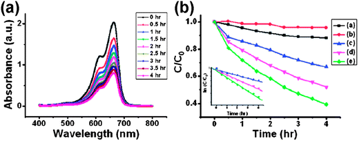 | ||
| Fig. 6 (a) Absorption spectrum of methylene blue (MB) solution in the presence of ZnS:Ga nanowalls under exposure to UV light for various durations. The decrease in the intensity of absorbance peaks at 664 nm is attributed to the decomposition of MB. (b) Variation with time of photodegradation of MB under different conditions: (a) ZnS:Ga nanowalls, dark, (b) without catalysts, under UV light, (c) ZnS:Ga film, under UV light, (d) P25 TiO2 film, under UV light, and (e) ZnS:Ga nanowalls, under UV light. The inset in (b) shows the data plotted into logarithmic scale. The data fit well with the equation of first order reaction kinetics.11 | ||
Photoelectric properties
To date, nanomaterial-based gas, chemical, biological and optical sensors have been fabricated and studied with respect to their optical and electrical properties. SnS is an important IV–VI group semiconductor material with a band gap of 1.33 eV. It belongs to the group of layered semiconductor materials. In particular, SnS has attracted much attention due to its potential applications in near-infrared detectors, photovoltaic materials with high conversion efficiency, and photoconductors.61a As important II–VI semiconductor materials, ZnS and CdS nanostructures have attracted much attention due to their excellent photoelectrical properties that make them promising nanomaterials for photovoltaics and photodetectors.61b,62 We have reported intercrossed sheet-like ZnS nanostructures with Ga dopant (ZnS:Ga nanowalls) grown on Si substrates by thermal evaporation of the mixed powders of ZnS and Ga2O3via a self-catalyzed growth mechanism.11 As shown in Fig. 7 and 8, the photoresponse of ZnS:Ga nanowalls shows superior photoconductive properties due to their high surface area and unique morphology. The increased conductivity of metal–semiconductor–metal (Ag–ZnS:Ga nanowalls-Ag) Schottky photodetectors under light illumination is attributed to the lowering of the Schottky barrier height, photogenerated electron–hole pairs, and the desorption of oxygen molecules on the ZnS:Ga surface. Because of the high photosensitivity and fast response, ZnS and the doped semiconducting metal sulfide nanostructures are promising materials systems for optical switches, sensors and photodetectors in the visible light region.63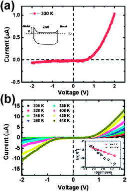 | ||
| Fig. 7 (a) Typical current–voltage curves of ZnS:Ga nanowall metal–semiconductor–metal (MSM) photodetectors measured at room temperature. The inset shows the band diagram of metal–ZnS–metal with different Schottky barrier heights at two contacts under zero bias. Ψ is the Schottky barrier height at the metal/ZnS interface. (b) The temperature dependent I–V characteristics of ZnS:Ga nanowall MSM photodetectors measured at temperatures between 300 and 448 K. The inset is the plot of ln (I/T2) versus 1/T at V = +1 and −1 V and the effective Schottky barrier heights are extracted to be 0.16 and 0.39 eV, respectively.11 | ||
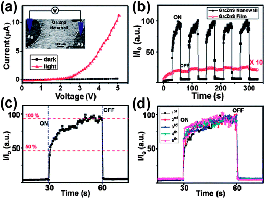 | ||
| Fig. 8 (a) Current–voltage (I–V) curves of the ZnS:Ga nanowall photoconductor measured in the dark and upon light illumination with a sweep voltage from 0 to 5 V. The inset is a schematic illustration of the ZnS:Ga nanowall photoconductor configuration. (b) The photoresponse of ZnS:Ga nanowall (black square line) and film (red circle line) for five cycles. Each interval is 30 s. I0 is the dark current at T = 0 s. (c) The detailed photoresponse of a single cycle, indicating the fast response and recovery time of ZnS:Ga nanowalls. (d) The combined photoresponse curves showing the consistency for different cycles.11 | ||
Thermoelectric properties
Nanoscale thermoelectric elements have demonstrated the ability to substantially increase the thermoelectric figure of merit beyond what is achievable with the bulk counterparts. Much research still needs to be done in order to obtain nanostructures which possess the right characteristics. Metal sulfide nanomaterials, such as bismuth sulfide (Bi2S3), antimony sulfide (Sb2S3) and lead sulfide (PbS) nanostructures, have recently attracted increasing interests due to their potential applications in the thermoelectric field. Bi2S3 and Sb2S3 are semiconducting materials with a direct band gap of 1.3 eV and 1.78 eV, respectively. They belong to the family of compounds M2X3 (where M = Bi, Pb, Sb and X = S, Se, Te), which are considered to be the potential materials for thermoelectric applications.64,65 The theoretical predictions and subsequent experimental results have proved the possibility of a significant enhancement in the thermoelectric figure of merit ZT in superlattices based on lead chalcogenide compounds.66 The thermoelectric power factor of these metal sulfide nanostructures is larger than that of their bulk counterparts and comparable to that of top state-of-the-art materials. These metal sulfide thermoelectric nanomaterials have great potential applications in solid-state power generation from heat sources.67Applications in energy conversion and storage
Lithium-ion batteries
Much novel research and important progress have been made in the development of advanced energy conversion and storage technologies due to the increasing demand for depletion of oil and environmental issues. Undoubtedly, lithium-ion batteries have long been considered an attractive rechargeable power source for consumer electronic products because of their advantages such as low-cost, light-weight, highly efficient and environmental friendliness.68 Among the various candidates for cathode materials, metal sulfides are suitable cathode materials for lithium-ion batteries because of their high theoretical capacity, high lithium activity and low cost.69,70 They are abundant and cheap due to the existence of minerals in nature. The reactions of transition metal chalcogenide electrodes involve two or more electrons per 3d metal as compared with only one of the commonly used commercial electrodes. In addition, the potential of the transition metal sulfidesversuslithium conversion process reactions depends on the ionocovalence of the bonding between the transition metal and the chalcogenide, and therefore can be tuned continuously from 0 to 3.5 V by changing the nature of the anion chalcogenide.71a Layered transition-metal dichalcogenides, such as WS2, MoS2 and SnS2, are of particular interest due to their special structural properties.71b,cSnS2 has a layered CdI2-type structure which is composed of tin atoms sandwiched between two layers of hexagonally close-packed sulfur atoms.70 The two-dimensional layered characteristics of these lamellar compounds are advantageous to alkali metal intercalation phenomena.One-dimensional nanowire arrays are promising electrode materials for lithium-ion batteries. The one-dimensional nanostructured electrode has several advantages. First, there is high contact area between the nanostructured electrode and electrolyte so that higher charge/discharge rates can be performed. Second, the small nanowire diameter allows for improved cycle life with better flexibility for accommodating the strain of lithium ions insertion/extraction without the fracture that can occur in micron-sized or bulk materials. Finally, short path distances allow for efficient charge transport of electrons from the current collector and lithium ions from the electrolyte.72 Direct growth of nanowire arrays onto working electrodes of lithium-ion batteries has many advantages. It can make better and larger contact between the nanostructured material and working electrode leading to easier transportation for electrons, simplify the cell assembly resulting in improvements of the time, yield rate and cost saving.73
We have used nickel sulfide and copper sulfide nanowire arrays which were directly grown on metal current collector substrates by a general solution route as working cathodes of lithium-ion batteries.7,27Fig. 9 shows the cycle performances and the variation of the normalized capacity with respect to the C-rate of the (a) Ni3S2 and (b) Cu2S nanowire arrays/Li cells cycled at ambient temperature. LiCoO2 is the commonly used cathode material in commercial lithium-ion batteries. The theoretical capacity of LiCoO2 is 145mA h g−1 and can be regarded as the criterion for the cathode material. Therefore, the capacity of the Ni3S2 and Cu2S nanowire arrays derived here can be close to 2.5 and 1.6 times of the LiCoO2, respectively. It is believed that the superior rate capability is attributed to better accommodation of the strain of lithium insertion/extraction and the higher electrode/electrolyte contact area.72,73 These experimental results demonstrate that better rate capability property is feasible by using nanostructured electrodes and indicating that one-dimensional nanowire arrays are effective at higher C-rates. As compared to the Ni3S2 and Cu2S thin film/Li cell or reports of powder electrodes,26,69 the higher reversible lithium storage capacity, longer cycle life, better cyclic stability and superior rate capability have demonstrated that the one-dimensional metal sulfide nanowire arrays, such as Ni3S2 and Cu2S, are potential storage materials as the cathodes for practical use in the next generation lithium-ion batteries.
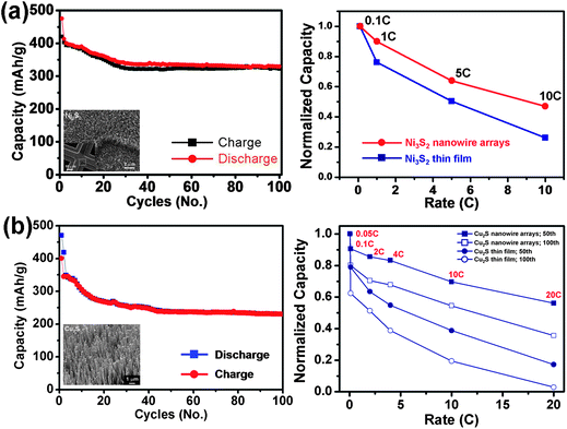 | ||
| Fig. 9 Cycle performances and profiles of the normalized capacity with respect to the C-rate of the (a) Ni3S2 and (b) Cu2S nanowire arrays/Li cells cycled at ambient temperature.7,27 | ||
Fuel cells
Fuel cells have many advantages, such as high energy storage and rapid recharge time. Solid oxide fuel cells (SOFCs) are flexible fuel cells with respect to fuel selection. They have great potential for power generation from alternative fuels including hydrocarbons, biogas and syngas.74 Anode poisoning caused by H2S in commercially available hydrocarbon resource-derived fuels is one of the major challenges for extended fuel applications in SOFCs. It is highly desirable to develop new anode materials with high catalytic activity and good sulfur tolerance for SOFCs.75,76 Transition metal sulfides, such as NiS and CoS, have been investigated as potential candidates for sulfur-tolerance anode materials for SOFCs.47 In addition, there is a strong motivation to find alternative cathode materials for proton-exchange-membrane fuel cells (PEMFCs), which are less expensive and more active than platinum. Co9S8 has been theoretically studied for its catalytic activity in O2 electroreduction.77aHydrogen is proposed as a major energy carrier for the future. Water is the most desirable source of hydrogen and it contains no carbon. Ni based catalyses are often employed in commercial alkaline electrolyzers for the hydrogen evolution reaction. Pt and its composites are the most active catalysts for hydrogen evolution. However, the large scale application of Pt catalysts is limited by their low abundance and high cost.77b Recently, amorphous molybdenum sulfide films for efficient hydrogen evolution catalysis in water have been reported. The catalysts are prepared in a simple, rapid, and scalable manner at atmospheric pressure and room temperature. The catalysis is compatible with a wide range of pHs from 0 to 13. Using these catalysts, significant geometric current densities are achieved at low overpotentials. The amorphous molybdenum sulfide films are among the most active non-precious catalysts for hydrogen evolution reactions.77c With the unique characteristics of nanostructured materials, metal sulfide nanostructures have attracted interests in high-performance fuel cells and nanosized power sources.78Hydrogen is considered one of the ideal alternative fuels due to its highly abundant, lightweight and non-polluting nature, but storage remains a problem and less than 1% is present as molecular hydrogen gas, H2.14,15 The development of hydrogen storage technology with a safe, effective, and inexpensive system for hydrogen fuel cells with a desired density is difficult. Most of the hydrogen is chemically bound as H2O in water and some is bound to liquid or gaseous hydrocarbons.79 Many alloys are capable of reversibly storing hydrogen through absorbing gaseous hydrogen at certain temperature and pressure to form metal hydrides.80 In addition to the gas-phase reaction, hydrogen can also be stored in nanostructured materials through electrochemical processes in aqueous solutions under moderate conditions. Nanostructured metal sulfide materials, such as MoS2 nanotubes and Bi2S3 nanorods, have attracted much attention for electrochemical hydrogen storage because of their unique characteristics such as large surface area, high surface reactivity and strong gas adsorption.81,82 In comparison with conventional low temperature–high pressure hydrogen storage technology, electrochemical hydrogen storage is a more convenient and efficient method for hydrogen storage at ambient temperature and pressure, by which hydrogen is absorbed in electrode materials during electrochemical decomposition of water. This method has been widely used in nickel/metal hydride accumulators.14 The novel metal sulfide nanostructures may find potential applications in hydrogen storage and high-energy batteries because of their fast sorption kinetics, high tolerance to recycling and high volumetric/gravimetric capacity.
Solar cells
Solar energy is the most environmentally friendly and technologically promising of the alternative energy sources. Cu2S is a p-type semiconducting material with an indirect bandgap of 1.21 eV. The earliest thin-film solar cells were based on CdS/Cu2S heterojunctions and the efficiencies could be reached up to ∼10% in the early 1980s.83 CdS/Cu2S solar cells showed significant potential in thin-film studies, however, the instability of the heterojunction due to Cu+ ions diffusion and doping of the CdS layer led to long-term performance degradation.84 With the progress of nanotechnologies and nanocrystal-based approaches, Cu2S nanocrystals in combination with CdS nanorods have been demonstrated in their application as solution-processed solar cells on both flexible plastic substrates and usual glass substrates with long-term stability.16,85 In addition, Cu2S can be used as an ideal light absorbing material in extremely thin absorber (ETA) solar cells due to its non-toxicity, low cost, abundance and good absorption characteristics.84The ternary I–III–VI2 chalcogenide chalcopyrites (CuMX2) (M = In, Ga and X = S, Se) have been developed with their power efficiencies now approaching 20%.17,86–88 These chalcopyrite compound materials possess advantages for photovoltaic applications: (i) they are direct bandgap semiconducting materials with corresponding high optical absorption coefficients, (ii) their bandgap energy is at the red edge of the solar spectrum, and (iii) they are stable under long-term excitation. Metal sulfide nanostructures can also be applied in dye-sensitized solar cells (DSSCs) because of high optical absorption coefficient and low cost.89,90 FeS, FeS2 and NiS nanostructures have been reported as novel photocathodes in tandem solar cells with dye-sensitized TiO2 nanostructures as the corresponding photoanode.91,92 Because of the unique electronic features which are due to the large band edge excitation of the metal centered d–d transition, layered metal sulfide semiconducting nanomaterials such as MoS2 and WS2 have been investigated for use in solar cells, photoelectrochemical, photovoltaic and photoelectrolysis cells.93a,b
Nanogenerators
Recently, nanogenerators based on wurtzite-structured nanomaterials, such as ZnO, GaN and InN nanowire arrays, have been demonstrated for converting mechanical energy into electric energy by utilizing the coupling effects of their semiconducting and piezoelectric properties.3,94–97 Among wurtzite-structured metal sulfide nanomaterials, CdS nanowire arrays were also successfully demonstrated for piezoelectric nanogenerators.98,99 As another member in the wurtzite family, ZnS is an important semiconducting, piezoelectric and optoelectric material. We have reported the synthesis of axial heterostructured ZnO–ZnS nanowire arrays for the first time by a thermal evaporation process in the presence of residual oxygen and demonstrated the first application of heterostructured ZnO–ZnS and ZnS nanowire arrays for converting mechanical energy into electricity.35Piezoelectric responses of the heterostructured ZnO–ZnS and ZnS nanowire arrays were examined using AFM in contact mode. The experimental setup is the same as first used demonstrating the piezoelectric nanogenerator.3 Applications of ZnO–ZnS heterojuction and ZnS nanowire arrays for energy generation are shown in Fig. 10 and 11, respectively. The AFM tip scanned across the samples to bend the nanowires and output electrical signals were continuously monitored. The process for generating electrical signals can be derived from detailed analyses of the topological profile and output voltage peak received by the tip when scanned across nanowires. As proposed previously for ZnO and CdS nanowires,3,98 the physical principle for creating electric potential in the nanowires arises from the materials' piezoelectric property, an effective charge accumulation and output is governed by its semiconducting property and Schottky contact with the tip. The results fully support the proposed energy converting mechanism for a piezoelectric nanogenerator.100,101 The significant discovery of a piezoelectric nanogenerator not only stimulates other promising applications of nanomaterials but also provides possibilities for building self-powering nanosystems in the future.102,103
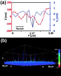 | ||
| Fig. 10 Application of ZnO–ZnS heterojuction NW arrays for energy generation. (a) Topography (red curve with filled squares) and voltage output (blue curve with open squares) line profiles across a heterostructure ZnO–ZnS NW array received by a conductive AFM tip. (b) Three-dimensional output of the voltage output image received from the AFM scan across a heterostructure ZnO–ZnS NW array with an area of 30 × 30 μm2.35 | ||
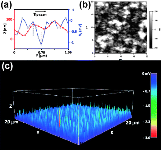 | ||
| Fig. 11 Application of ZnS NW arrays for energy generation. (a) Topography (red curve with filled squares) and voltage output (blue curve with open squares) line profiles across ZnS NW arrays. (b and c) Topography and the corresponding output voltage images were recorded simultaneously, respectively, when the AFM tip was scanned over the aligned ZnS NW arrays.35 | ||
Summary and future outlook
Metal sulfide nanostructures are important nanomaterials due to their extensively promising applications in electronic, optical, optoelectronic and magnetic devices. The aligned nanostructure arrays on substrates are highly attractive due to their enhanced properties and novel applications. In the 21st century, energy shortage and global warming are two great challenges to human beings. The demand for development of efficient and clean alternative energies has become the most urgent research field. In this article, we have presented an overview of recent research work regarding metal sulfide nanostructures and significant advances reported in the literature, covering from synthesis to properties and to applications especially in energy conversion and storage, such as lithium-ion batteries, solar cells, fuel cells and piezoelectric nanogenerators. Those novel synthetic methods, excellent properties and extensive applications will be of great importance in many areas.In order to satisfy today's information-rich and mobile society, there are huge demands for high-performance and multi-function devices for computers, communications and consumer electronics. The unique setting of well-aligned nanostructures on substrates has facilitated the studies on properties and applications. In addition to the enhanced performance, new functions through doping and development of clean alternative energies may be exploited for various applications of metal sulfide nanostructures. They present ample opportunities for scientists and technologists to engage in the research and development of nanostructured materials. Nanodevices with nanostructured metal sulfide materials have been demonstrated, especially in energy conversion and storage to confront grand challenges of energy shortage and global warming. With the rapid development of nanotechnology and increasing attention from the industry, it is expected that commercial applications will be realized soon.
Acknowledgements
The authors would like to thank Dr K. W. Huang for his contributions to the work reviewed in this article. The work was supported by the Republic of China National Science Council through grant no. NSC 98-2221-E-007-104-MY3.References
- A. P. Alivisatos, Science, 1996, 271, 933 CrossRef CAS.
- D. D. D. Ma, C. S. Lee, F. C. K. Au, S. Y. Tong and S. T. Lee, Science, 2003, 299, 1874 CrossRef CAS.
- Z. L. Wang and J. H. Song, Science, 2006, 312, 242 CrossRef CAS.
- X. S. Fang, Y. Bando, U. K. Gautam, T. Zhai, S. Gradecak and D. Golberg, J. Mater. Chem., 2009, 19, 5683 RSC.
- K. C. Chen, W. W. Wu, C. N. Liao, L. J. Chen and K. N. Tu, Science, 2008, 321, 1066 CrossRef CAS.
- M. Law, L. E. Greene, J. C. Johnson, R. Saykally and P. D. Yang, Nat. Mater., 2005, 4, 455 CrossRef CAS.
- C. H. Lai, K. W. Huang, J. H. Cheng, C. Y. Lee, B. J. Hwang and L. J. Chen, J. Mater. Chem., 2010, 20, 6638 RSC.
- (a) L. J. Chen, J. Mater. Chem., 2007, 17, 4639 RSC; (b) L. J. Chen, JOM, 2005, 57(9), 24 CrossRef CAS; (c) L. J. Chen and W. W. Wu, Mater. Sci. Eng., R, 2010, 70, 303 CrossRef.
- K. W. Huang, J. H. Wang, H. C. Chen, H. C. Hsu, Y. C. Chang, M. Y. Lu, C. Y. Lee and L. J. Chen, J. Mater. Chem., 2007, 17, 2307 RSC.
- Z. H. Wen and J. H. Li, J. Mater. Chem., 2009, 19, 8707 RSC.
- M. Y. Lu, M. P. Lu, Y. A. Chung, M. J. Chen, Z. L. Wang and L. J. Chen, J. Phys. Chem. C, 2009, 113, 12878 CrossRef CAS.
- J. Liu, G. Z. Cao, Z. G. Yang, D. H. Wang, D. Dubois, X. D. Zhou, G. L. Graff, L. R. Pederson and J. G. Zhang, ChemSusChem, 2008, 1, 676 CrossRef CAS.
- Y. Wang and G. Z. Cao, Adv. Mater., 2008, 20, 2251 CrossRef CAS.
- L. Schlapbach and A. Zuttel, Nature, 2001, 414, 353 CrossRef.
- Q. F. Zhang and G. Z. Cao, J. Mater. Chem., 2011, 21, 6769 RSC.
- Y. Wu, C. Wadia, W. L. Ma, B. Sadtler and A. P. Alivisatos, Nano Lett., 2008, 8, 2551 CrossRef CAS.
- T. L. Li, Y. L. Lee and H. S. Teng, J. Mater. Chem., 2011, 21, 5089 RSC.
- M. J. Bierman and S. Jin, Energy Environ. Sci., 2009, 2, 1050 RSC.
- D. Moore and Z. L. Wang, J. Mater. Chem., 2006, 16, 3898 RSC.
- X. S. Fang, Y. Bando, G. Z. Shen, C. H. Ye, U. K. Gautam, P. M. F. J. Costa, C. Y. Zhi, C. C. Tang and D. Golberg, Adv. Mater., 2007, 19, 2593 CrossRef CAS.
- T. Sakamoto, H. Sunamura, H. Kawaura, T. Hasegawa, T. Nakayama and M. Aono, Appl. Phys. Lett., 2003, 82, 3032 CrossRef CAS.
- J. Liu and D. F. Xue, J. Mater. Chem., 2011, 21, 223 RSC.
- F. Cao, R. X. Liu, L. Zhou, S. Y. Song, Y. Q. Lei, W. D. Shi, F. G. Zhao and H. J. Zhang, J. Mater. Chem., 2010, 20, 1078 RSC.
- W. Zhang, Y. B. Wang, Z. Wang, Z. Y. Zhong and R. Xu, Chem. Commun., 2010, 46, 7631 RSC.
- P. A. Metcalf, B. C. Crooker, M. McElfresh, Z. Kakol and J. M. Honig, Phys. Rev. B: Condens. Matter, 1994, 50, 2055 CrossRef CAS.
- X. J. Zhu, Z. Y. Wen, Z. H. Gu and S. H. Huang, J. Electrochem. Soc., 2006, 153, A504 CrossRef CAS.
- C. H. Lai, K. W. Huang, J. H. Cheng, C. Y. Lee, W. F. Lee, C. T. Huang, B. J. Hwang and L. J. Chen, J. Mater. Chem., 2009, 19, 7277 RSC.
- R. F. Heidelberg, A. H. Luxem, S. Talhouk and J. J. Banewicz, Inorg. Chem., 1996, 5, 194.
- J. Wang, S. H. Ng, G. X. Wang, J. Chen, L. Zhao, Y. Chen and H. K. Liu, J. Power Sources, 2006, 159, 287 CrossRef CAS.
- Y. Jiang, W. J. Zhang, J. S. Jie, X. M. Meng, J. A. Zapien and S. T. Lee, Adv. Mater., 2006, 18, 1527 CrossRef CAS.
- L. Z. Zhang, J. C. Yu, M. S. Mo, L. Wu, Q. Li and K. W. Kwong, J. Am. Chem. Soc., 2004, 126, 8116 CrossRef CAS.
- C. Mao, D. J. Solis, B. D. Reiss, S. T. Kottmann, R. Y. Sweeney, A. Hayhurst, G. Georgiou, B. Iverson and A. M. Belcher, Science, 2004, 303, 213 CrossRef CAS.
- (a) Q. Y. Lu, F. Gao and S. Komarneni, J. Am. Chem. Soc., 2004, 126, 54 CrossRef CAS; (b) C. Bartels, R. Cooper, D. J. Auerbach and A. M. Wodtke, Chem. Sci., 2011, 2, 1647 RSC.
- M. Y. Lu, L. J. Chen, W. J. Mai and Z. L. Wang, Appl. Phys. Lett., 2008, 93, 242503 CrossRef.
- M. Y. Lu, J. H. Song, M. P. Lu, C. Y. Lee, L. J. Chen and Z. L. Wang, ACS Nano, 2009, 3, 357 CrossRef CAS.
- (a) E. P. T. Tyndall, Phys. Rev., 1923, 21, 162 CrossRef CAS; (b) L. Li, P. C. Wu, X. S. Fang, T. Y. Zhai, L. Dai, M. Y. Liao, Y. Koide, H. Q. Wang, Y. Bando and D. Golberg, Adv. Mater., 2010, 22, 3161 CrossRef CAS; (c) J. F. Hall, J. Opt. Soc. Am., 1956, 46, 1013 CrossRef CAS.
- L. W. Yin and S. T. Lee, Nano Lett., 2009, 9, 957 CrossRef CAS.
- Y. K. Liu, J. A. Zapien, Y. Y. Shan, C. Y. Geng, C. S. Lee and S. T. Lee, Adv. Mater., 2005, 17, 1372 CrossRef CAS.
- A. L. Pan, H. Yang, R. B. Liu, R. C. Yu, B. S. Zou and Z. L. Wang, J. Am. Chem. Soc., 2005, 127, 15692 CrossRef CAS.
- M. Y. Lu, P. Y. Su, Y. L. Chueh, L. J. Chen and L. J. Chou, Appl. Surf. Sci., 2005, 244, 96 CrossRef CAS.
- X. Wu, P. Jiang, Y. Ding, W. Cai, S. S. Xie and Z. L. Wang, Adv. Mater., 2007, 19, 2319 CrossRef CAS.
- (a) X. Fan, M. L. Zhang, I. Shafiq, W. J. Zhang, C. S. Lee and S. T. Lee, Adv. Mater., 2009, 21, 2393 CrossRef CAS; (b) S. J. Xu, S. J. Chua, B. Liu, L. M. Gan, C. H. Chew and G. Q. Xu, Appl. Phys. Lett., 1998, 73, 478 CrossRef CAS; (c) N. E. Hsu, W. K. Hung and Y. F. Chen, J. Appl. Phys., 2004, 96, 4671 CrossRef CAS.
- (a) X. L. Yu, Y. Wang, R. K. Zheng, J. F. Qu, H. L. W. Chan and C. B. Gao, Cryst. Growth Des., 2009, 9, 1293 CrossRef CAS; (b) W. Han and M. Y. Gao, Cryst. Growth Des., 2008, 8, 1023 CrossRef CAS.
- P. V. Radovanovic, C. J. Barrelet, S. Gradecak, F. Qian and C. M. Lieber, Nano Lett., 2005, 5, 1407 CrossRef.
- S. A. Wolf, D. D. Awschalom, R. A. Buhrman, J. M. Daughton, S. V. Molnar, M. L. Roukes, A. Y. Chtchelknova and D. M. Treger, Science, 2001, 294, 1488 CrossRef CAS.
- J. K. Furdyna, J. Appl. Phys., 1988, 64, R29 CrossRef CAS.
- C. M. Grgicak and J. B. Giorgi, J. Phys. Chem. C, 2007, 111, 15446 CrossRef CAS.
- Z. W. Wang, L. L. Daemen, Y. S. Zhao, C. S. Zha, R. T. Downs, X. D. Wang, Z. L. Wang and R. J. Hemley, Nat. Mater., 2005, 4, 922 CrossRef CAS.
- G. D. Yuan, W. J. Zhang, W. F. Zhang, X. Fan, I. Bello, C. S. Lee and S. T. Lee, Appl. Phys. Lett., 2008, 93, 213102 CrossRef.
- Z. B. He, J. S. Jie, W. J. Zhang, W. F. Zhang, L. B. Luo, X. Fan, G. D. Yuan, I. Bello and S. T. Lee, Small, 2009, 5, 345 CrossRef CAS.
- L. Li, Y. Zhang, X. S. Fang, T. Y. Zhai, M. Y. Liao, X. L. Sun, Y. Koide, Y. Bando and D. Golberg, J. Mater. Chem., 2011, 21, 6525 RSC.
- X. S. Fang, Y. Bando, U. K. Gautam, C. H. Ye and D. Golberg, J. Mater. Chem., 2008, 18, 509 RSC.
- J. Chen, S. Z. Deng, J. C. She, N. S. Xu, W. X. Zhang, X. G. Wen and S. H. Yang, J. Appl. Phys., 2003, 93, 1774 CrossRef CAS.
- U. K. Gautam, X. S. Fang, Y. Bando, J. H. Zhan and D. Golberg, ACS Nano, 2008, 2, 1015 CrossRef CAS.
- T. Y. Zhai, X. S. Fang, Y. Bando, Q. Liao, X. J. Xu, H. B. Zeng, Y. Ma, J. N. Yao and D. Golberg, ACS Nano, 2009, 4, 949 CrossRef.
- V. J. Gandubert, E. Torres and C. M. Niemeyer, J. Mater. Chem., 2008, 18, 3824 RSC.
- Q. F. Han, L. Chen, M. J. Wang, X. J. Yang, L. D. Lu and X. Wang, Mater. Sci. Eng., B, 2010, 166, 118 CrossRef CAS.
- M. Muruganandham and Y. Kusumoto, J. Phys. Chem. C, 2009, 113, 16144 CrossRef CAS.
- H. W. Park, W. Y. Choi and M. R. Hoffmann, J. Mater. Chem., 2008, 18, 2379 RSC.
- Y. X. Li, G. Chen, C. Zhou and J. X. Sun, Chem. Commun., 2009, 2020 RSC.
- (a) S. K. Panda, A. Datta, A. Dev, S. Gorai and S. Chaudhuri, Cryst. Growth Des., 2006, 6, 2177 CrossRef CAS; (b) X. S. Fang, Y. Bando, M. Y. Liao, U. K. Gautam, C. Y. Zhi, B. Dierre, B. D. Liu, T. Y. Zhai, T. Sekiguchi, Y. Koide and D. Golberg, Adv. Mater., 2009, 21, 2034 CrossRef CAS.
- L. Li, P. Wu, X. S. Fang, T. Y. Zhai, L. Dai, M. Liao, Y. Koide, H. Q. Wang, Y. Bando and D. Golberg, Adv. Mater., 2010, 22, 3161 CrossRef CAS.
- E. Monroy, F. Omnes and F. Calle, Semicond. Sci. Technol., 2003, 18, R33 CrossRef CAS.
- S. C. Liufu, L. D. Chen, Q. Yao and C. F. Wang, Appl. Phys. Lett., 2007, 90, 112106 CrossRef.
- R. Malakooti, L. Cademartiri, A. Migliori and G. A. Ozin, J. Mater. Chem., 2008, 18, 66 RSC.
- T. C. Harman, P. J. Taylor, M. P. Walsh and B. E. LaForge, Science, 2002, 297, 2229 CrossRef CAS.
- L. D. Hicks and M. S. Dresselhaus, Phys. Rev. B: Condens. Matter, 1993, 47, 12727 CrossRef CAS.
- C. H. Jiang, E. Hosono and H. S. Zhou, Nano Today, 2006, 1, 28 CrossRef.
- S. C. Han, H. S. Kim, M. S. Song, J. H. Kim, H. J. Ahn and J. Y. Lee, J. Alloys Compd., 2003, 351, 273 CrossRef CAS.
- J. W. Seo, J. T. Jang, S. W. Park, C. Kim, B. Park and J. Cheon, Adv. Mater., 2008, 20, 4269 CrossRef CAS.
- (a) H. Li, P. Balaya and J. Maier, J. Electrochem. Soc., 2004, 151, A1878 CrossRef CAS; (b) A. Rothschild, J. Sloan and R. Tenne, J. Am. Chem. Soc., 2000, 122, 5169 CrossRef CAS; (c) Y. F. Shi, Y. Wan, R. L. Liu, B. Tu and D. Y. Zhao, J. Am. Chem. Soc., 2007, 129, 9522 CrossRef CAS.
- C. K. Chan, H. Peng, G. Liu, K. McIlwrath, X. F. Zhang and Y. Cui, Nat. Nanotechnol., 2008, 3, 31 CrossRef CAS.
- N. S. Choi, Y. Yao, Y. Cui and J. Cho, J. Mater. Chem., 2011, 21, 9825 RSC.
- B. C. H. Steele and A. Heinzel, Nature, 2001, 414, 345 CrossRef CAS.
- C. Peng, J. L. Luo, A. R. Sanger and K. T. Chuang, Chem. Mater., 2010, 22, 1032 CrossRef CAS.
- L. Yang, Z. Cheng, M. L. Liu and L. Wilson, Energy Environ. Sci., 2010, 3, 1804 RSC.
- (a) R. A. Sidik and B. Anderson, J. Phys. Chem. B, 2006, 110, 936 CrossRef CAS; (b) P. Millet, F. Andolfatto and R. Durand, Int. J. Hydrogen Energy, 1996, 21, 87 CrossRef CAS; (c) D. Merki, S. Fierro, H. Vrubel and X. Hu, Chem. Sci., 2011, 2, 1262 RSC.
- C. F. Pan, H. Wu, C. Wang, B. Wang, L. Zhang, Z. D. Cheng, P. Hu, W. Pan, Z. Y. Zhou, X. Yang and J. Zhu, Adv. Mater., 2008, 20, 1644 CrossRef CAS.
- G. D. Dai, C. Liu, M. Liu, M. Z. Wang and H. M. Cheng, Nano Lett., 2002, 2, 503 CrossRef CAS.
- A. Baldi and B. Dam, J. Mater. Chem., 2011, 21, 4021 RSC.
- J. Chen, N. Kuriyama, H. T. Yuan, H. T. Takeshita and T. Sakai, J. Am. Chem. Soc., 2001, 123, 11813 CrossRef CAS.
- B. Zhang, X. C. Ye, W. Y. Hou, Y. Zhao and Y. Xie, J. Phys. Chem. B, 2006, 110, 8978 CrossRef CAS.
- J. A. Bragangolo, A. M. Barnett, J. E. Phillips, R. B. Hall, A. Rothwarf and J. D. Meakin, IEEE Trans. Electron Devices, 1980, 27, 645 CrossRef.
- M. Page, O. Niitsoo, Y. Itzhaik, D. Cahen and G. Hodes, Energy Environ. Sci., 2009, 2, 220 RSC.
- X. M. Li, H. B. Shen, S. Li, J. Z. Niu, H. Z. Wang and L. S. Li, J. Mater. Chem., 2010, 20, 923 RSC.
- M. G. Panthani, V. Akhavan, B. Goodfellow, J. P. Schmidtke, L. Dunn, A. Dodabalapur, P. F. Barbara and B. A. Korgel, J. Am. Chem. Soc., 2008, 130, 16770 CrossRef CAS.
- D. B. Mitzi, M. Yuan, W. Liu, A. J. Kellock, S. J. Chey, V. Deline and A. G. Schrott, Adv. Mater., 2008, 20, 3657 CrossRef CAS.
- L. Li, N. Coates and D. Moses, J. Am. Chem. Soc., 2010, 132, 22 CrossRef CAS.
- Y. K. A. Lau, D. J. Chernak, M. J. Bierman and S. Jin, J. Mater. Chem., 2009, 19, 934 RSC.
- F. Zhang and S. S. Wong, Chem. Mater., 2009, 21, 4541 CrossRef CAS.
- Y. Hu, Z. Zheng, H. M. Jia, Y. W. Tang and L. Z. Zhang, J. Phys. Chem. C, 2008, 112, 13037 CrossRef CAS.
- H. C. Sun, D. Qin, S. Q. Huang, X. Z. Guo, D. M. Li, Y. H. Luo and Q. B. Meng, Energy Environ. Sci., 2011, 4, 2630 Search PubMed.
- (a) M. T. Spitler and B. A. Parkinson, Acc. Chem. Res., 2009, 42, 2017 CrossRef CAS; (b) C. L. Stender, E. C. Greyson, Y. Babayan and T. W. Odom, Adv. Mater., 2005, 17, 2841 CrossRef CAS.
- X. D. Wang, J. H. Song and Z. L. Wang, J. Mater. Chem., 2007, 17, 711 RSC.
- M. P. Lu, J. H. Song, M. Y. Lu, M. T. Chen, Y. F. Gao, L. J. Chen and Z. L. Wang, Nano Lett., 2009, 9, 1223 CrossRef CAS.
- C. T. Huang, J. H. Song, W. F. Lee, Y. Dong, Z. Y. Gao, Y. Hao, L. J. Chen and Z. L. Wang, J. Am. Chem. Soc., 2010, 132, 4766 CrossRef CAS.
- C. T. Huang, J. H. Song, C. M. Tsai, W. F. Lee, D. H. Lien, Z. Y. Gao, Y. Hao, L. J. Chen and Z. L. Wang, Adv. Mater., 2010, 22, 4008 CrossRef CAS.
- Y. F. Lin, J. H. Song, Y. Ding, S. Y. Lu and Z. L. Wang, Appl. Phys. Lett., 2008, 92, 022105 CrossRef.
- Y. F. Lin, J. H. Song, Y. Ding, S. Y. Lu and Z. L. Wang, Adv. Mater., 2008, 20, 3127 CrossRef CAS.
- Z. L. Wang, Adv. Mater., 2007, 19, 889 CrossRef CAS.
- Z. L. Wang, Nano Today, 2010, 5, 540 CrossRef CAS.
- Z. L. Wang, Adv. Funct. Mater., 2008, 18, 1.
- S. Xu, B. J. Hansen and Z. L. Wang, Nat. Commun., 2010, 1, 93 Search PubMed.
| This journal is © The Royal Society of Chemistry 2012 |