The Mott transition and optimal performance of transparent conducting oxides in thin-film solar cells
Daniel
Slocombe
*a,
Adrian
Porch
a,
Michael
Pepper
b and
Peter P.
Edwards
c
aSchool of Engineering, Cardiff University, Queen's Buildings, The Parade, Cardiff, CF24 3AA, UK. E-mail: SlocombeDR@cardiff.ac.uk; PorchA@cardiff.ac.uk
bDepartment of Electronic and Electrical Engineering, University College London, Torrington Place, London WC1H 0AH, UK. E-mail: m.pepper@ee.ucl.ac.uk
cInorganic Chemistry Laboratory, University of Oxford, South Parks Road, Oxford, OX1 3QR, UK. E-mail: peter.edwards@chem.ox.ac.uk
First published on 8th November 2011
Abstract
The performance of thin-film solar cells is critically dependent upon the effective operation of transparent conducting oxide (TCO) layers, which play a significant role in both optical and electrical power transmission through these photovoltaic devices. In this article, we model the optical and electrical power transmission through TCO layers in thin-film solar cells as a function of both the electron carrier density, n, and its mobility, μ. The electrical and optical properties of the TCO layer are described by the simple Drude model of the degenerate free electron gas and the concomitant electromagnetic absorption due to skin-depth effects is thereby calculated. Above the critical carrier density for the composition-induced Mott Insulator-Conductor Transition, TCOs exhibit metallic-type conduction. However, with increasing electron (carrier) density above the transition, the optical transparency of the layer is significantly decreased. Importantly, in order to achieve high electrical conductivity whilst preserving high optical transparency of the TCO layer, electron mobilities need to be increased in preference to increasing electron densities. To reach higher carrier mobilities in any given TCO system, we propose that one should move the material close to the Mott transition. A model of ionized impurity scattering in indium tin oxide (ITO) at high carrier densities allows direct comparison of the μ-n relationship in real TCO layers to the total power absorption in such layers in thin-film solar devices. We determine that decreasing the electron density from 2.6 × 1021 cm−3 to 2 × 1021 cm−3 in such an ITO layer above the Mott critical density can decrease the total power absorption in the layer by a large amount (around 8% relative to the minimum theoretical absorption).
Broader contextThe production of high-performance transparent conducting oxides (TCO) is of critical importance to thin-film solar cells. The remarkable properties of both high conductivity and high transparency are however only achievable within certain limits. As dopant density is increased, a natural competition between these two critical performance indicators emerges. The challenge facing producers of TCOs is therefore to achieve high dopant densities for high conductivity, but low dopant densities for high transparency. Producers of TCOs must search closer to the Mott conductor-insulator transition for high-performance materials, where the low carrier density but high mobility is well suited to use in thin-film solar devices. As thin-film solar cells emerge as a possible alternative to silicon wafer based technology, the optimization of TCOs remains essential for the further proliferation of thin-film photovoltaics. This article considers the power absorption of an indium tin oxide layer in such a thin-film device and pursues optimal performance close to the Mott transition. |
Introduction
Transparent conducting oxides (TCO) find widespread use as transparent electrodes in optoelectronic devices.1 TCOs such as tin-doped indium oxide (ITO) and fluorine-doped tin oxide (FTO) are used as current collectors and form conducting layers in thin-film photovoltaic cells.2,3 The TCO layer influences the performance of such solar cell devices in two respects. Firstly, by transmission of the optical power of incident light through the layer. Secondly, by transmission of electrical power through the layer by the transport of the optically-generated carriers. Consequently, it is very important that the TCO layer has both a low sheet resistance Rsq and high optical transparency in order to optimize the output power of the device. Unfortunately, as we will illustrate, these parameters are in natural conflict.Since Rsq = 1/neμet, to reduce the sheet resistance one might increase the carrier density n, the carrier mobility μe, or the film thickness t. However, increasing n and μe also affects the electromagnetic skin depth δ, which is associated with absorption of electromagnetic radiation. This ultimately determines the optical transparency of the film since the optical power transmission coefficient is approximately proportional to exp(−2t/δ). For a given layer thickness, increasing the carrier density in any TCO system will therefore have the effect of increasing the conductivity, but also necessarily decreasing the transparency. In Fig. 1 we show the effect of increasing the electron density, for a material at carrier densities above the Mott Insulator-Conductor Transition, upon the dc electrical conductivity and optical transparency of a typical TCO layer, calculated using the simple Drude model as discussed in the following sections.
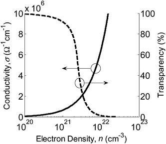 | ||
| Fig. 1 The effect of increasing the electron density upon conductivity (solid line) and transparency (dashed line) in a TCO layer at carrier densities above the Mott Insulator-Conductor Transition. For normally incident light of wavelength 800 nm, upon an ITO film of thickness 80 nm. | ||
Transparent conducting thin-films can therefore only be optimized for both low sheet resistance and high optical transparency by increasing the electron (carrier) mobility in preference to the carrier density.4 In the following sections, this will be shown to have a major effect upon the power absorption of the transparent conducting layer in photovoltaic cells. In the relationship5,6 between the mobility and carrier concentration shown in Fig. 2, we observe that higher mobilities may be achieved by moving the material closer to the Mott critical density, where reduced ionized-impurity scattering is exhibited at lower carrier densities. Then, for a given TCO system, this finding allows optimized values of both n and μe to be deduced for applications in solar energy devices. Photon absorption due to in-band states is ignored in this work under the assumption that this can be suppressed by appropriate materials processing.
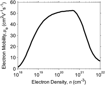 | ||
| Fig. 2 μ e–n relationship using the combined model proposed by Ellmer et al.7 and fitted to empirical data for ITO. | ||
Plotting the empirical curve proposed by Masetti et al.,6 for ionized impurity scattering in doped semiconductors and fitted to experimental values for ITO obtained by Ellmer et al.,7 an optimization in both parameters is demonstrated by comparison with power absorption curves for TCO photovoltaic device layers derived using the simple Drude model of optoelectronic properties above dopant levels set by the Mott criterion.8 Importantly, a carrier density reduction from 2.6 × 1021 cm−3 to 2 × 1021 cm−3 is shown to result in an decrease in total power absorption in the TCO layer of around 8% relative to the theoretical minimum absorption of ITO.
The μ-n relationship and the Mott critical density
To investigate the μ-n relationship in TCOs and the effects of this relationship upon optical power absorption in a thin-film solar cell, we first consider empirical models of scattering mechanisms for TCOs and related doped semiconductor systems. The behaviour of such TCOs will, of course, vary greatly from material to material and with different preparation methods. However, the exact behaviour does not influence our conclusions since the principle of optimization remains valid for any given TCO system under the influence of ionized impurity scattering above the Mott critical density.It is generally recognised that the dominant carrier scattering mechanism in ITO above n ≈ 3 × 1021 cm−3 is due to ionized impurities11 and with increasing carrier density, a decrease in carrier mobility is observed.5 This behaviour was modelled by Masetti et al.6 for carrier densities above the Mott critical density, and at densities of 1 × 1019 cm−3 by fitting experimental results for As, P and B doped Si to the empirical curve described by eqn (1),
 | (1) |
Below the Mott critical density the decrease in mobility may have a number of contributing causes. Ellmer et al.7 include the influence of grain barrier limited transport at lower carrier densities in their model of polycrystalline ITO, and Leenheer et al.5 attribute similar behaviour in amorphous indium zinc oxide films to a hopping (or percolation) type carrier transport and lattice scattering. In Fig. 2 we show the combined ionized and grain boundary model using the empirical parameters obtained for ITO.7 The electron mobility is limited above n ≈ 5 × 1020 cm−3 by electron-ion impurity scattering modelled by eqn (1) as described above,6 and below n ≈ 5 × 1020 cm−3 scattering is described by the model proposed by Seto et al.,12 though carrier densities down to this order are not considered in this work.
Optical properties of the free electron gas
The optical properties of ITO thin films above the Mott critical density are discussed in Porch et al.,9 within the framework of the simple Drude model where a parabolic conduction band is considered to be partially filled by a degenerate free electron gas. There is a strong frequency dependence of the scattering time τ for Fermi surface electrons10 in such a model, though if we consider only the visible part of the spectrum, τ is assumed to be approximately constant. The Drude form of the complex permittivity is ε = ε1 − jε2,13 thus giving | (2) |
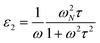 | (3) |
The skin depth and free electron absorption ultimately determine the transparency of sufficiently thick TCO layers. Calculations of the optical power transmission coefficient T can be carried out using the wavenumber k = ωε½/c and the plane wave impedance Z = ωμ0/k. The skin depth is defined using the wavenumber k by δ = −1/Im(k). This analysis gives
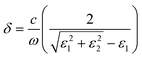 | (4) |
In Fig. 3 we show contours of normalized optical power transmission coefficient Topt = T(t)/T(0) as a function of μe and n, for normally incident, incoherent light of free space wavelength λ0 = 800nm and for an ITO film of thickness 80nm. The contours are normalized to the maximum theoretical optical power transmission, i.e. for t = 0, giving 100% transparency. For large values of n, the normalized optical power transmission coefficient becomes very small as the plasma frequency approaches the frequency of the incident light, since ωp ∝ n½. The increased values of Topt when μe < 10 cm2V−1s−1 correspond to increased values of δ, and is the result of ωp increasing with decreasing μe in this low mobility limit. Similar contours are obtained for both shorter wavelengths and decreased thicknesses, but increased values of Topt are exhibited as we move further above ωp and are less subject to skin depth effects as t is reduced.
 | ||
| Fig. 3 Normalized optical power transmission coefficient Topt (solid lines) as a function of electron density n and mobility μe for normally incident light of wavelength 800 nm upon an ITO film of 80 nm thickness. Dotted lines are contours of constant sheet resistance Rsq = 1/neμet (units of Ω). | ||
Implications for thin-film photovoltaic devices
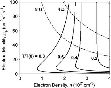
The power generated by a thin-film photovoltaic device is influenced by many layers and interfaces, but considering the TCO layer in isolation, and its optoelectronic performance, we can determine the total power absorption coefficient AT calculated relative to the minimum theoretical value for the layer. The optical power passing through the TCO layer of a photovoltaic cell is subject to the effects of electromagnetic absorption. The same layer is responsible for conducting generated current towards a metal contact. The total power transmission of the TCO layer is therefore proportional to the factor9,14TT = Telec × Topt = (nμet) × exp(−2t/δ), where the figure of merit Telec = (nμet) accounts for the increased spreading current as thickness t increases (assuming a rectangular contact geometry) and is the reciprocal of the sheet resistance. The term Topt = exp(−2t/δ) accounts for the increased electromagnetic absorption due to the skin depth. For incident light entering the TCO layer, we define the power absorption coefficient AT = 1 − TT. This is normalized to the minimum theoretical absorption for the layer dictated by the intrinsic mobility limit for ITO established by Bellingham et al.11 at around 100cm2V−1s−1. In Fig. 4 we show a schematic diagram of a typical thin-film solar module in superstrate configuration.2 The TCO layer spreads current between the rectangular contacts of each active cell in the solar module. The power absorption of the transparent conducting layer is decreased by increasing μe, but for varying n or t an optimum value exists which minimizes power absorption. This is demonstrated in Fig. 5, which plots normalized power absorption contours for normally incident incoherent light of free space wavelength λ0 = 800nm and for an ITO film of thickness 80nm (appropriate for antireflection purposes). Each value of μe has a corresponding, optimized value of n, which lies on the locus shown in Fig. 5 by a dashed line.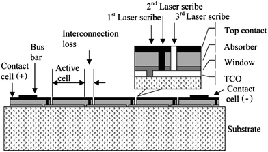 | ||
| Fig. 4 Schematic diagram of a typical thin-film photovoltaic module (from ref. 2). | ||
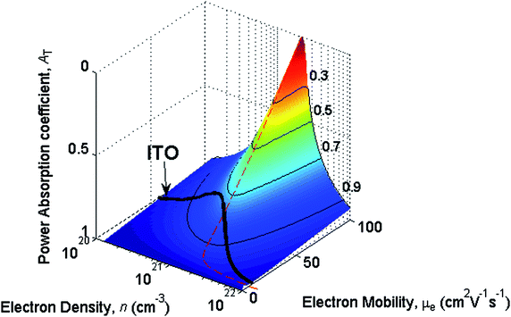 | ||
| Fig. 5 Contours of power absorption coefficient AT, normalized to the minimum theoretical value at μe = 100 cm2/Vs for an ITO layer in a thin-film photovoltaic cell. The film thickness is 80nm and incident wavelength λ0 = 800nm. Optimum carrier density for a given mobility is shown (red dashed line), which intersects the μe–n line describing ionized impurity scattering in ITO. | ||
Plotting the empirical model described by eqn (1) with parameters obtained experimentally allows a direct analysis of the free carrier behaviour for a given TCO system. In Fig. 5 the curve is plotted for an ITO system with empirical parameters obtained from ref. 7. It is observed that following the ITO curve towards lower electron densities by moving closer to the Mott critical density minimizes the total power absorption of the photovoltaic device layer. For example, decreasing n from 2.6 × 1021 cm−3 to 2 × 1021 cm−3, increases μe and decreases total power absorption by around 8%, a very significant result.
Summary and conclusions
Models of the μ-n relationship in transparent conducting oxides were considered using combined electron scattering models which have been fitted to experimental data for ITO. Above the Mott critical density for the Insulator-Conductor Transition, ionized impurity scattering causes a large decrease in electron mobility. It is suggested that to achieve high mobilities for a given TCO system, we must manipulate the material to move closer to the Mott critical density.The simple Drude model was used here to determine the electrical and optical properties of the TCO as a function of electron mobility and electron density. However, it is clear that these parameters are in natural conflict, since for increasing electron density, the conductivity is increased, but the optical transparency is reduced because of the electromagnetic absorption associated with the concomitant reduced skin depth. It has been proposed that properties for any TCO material may be improved by increasing mobility in preference to electron density. It was shown that this is particularly important for devices such as thin-film solar cells, in which the TCO layer must be both highly transparent and highly conducting.
Within the framework of the simple Drude model, power absorption coefficients for a TCO layer in a typical thin-film solar cell were calculated as functions of the mobilities and electron densities. Using the scattering model outlined above and fitted to experimental data for ITO, a direct observation was made of total power absorption in the layer for a real ITO system. It was shown that decreasing the electron density n from 2.6 × 1021 cm−3 to 2 × 1021 cm−3, increases μe and decreases total power absorption in the layer by around 8% relative to the theoretical minimum value. We believe that this highly significant result will allow optimization of the performance of a given TCO material in thin-film solar cells.
References
- C. G. Granqvist and A. Hultaker, Thin Solid Films, 2002, 411, 1 CrossRef CAS.
- K. L. Chopra, P. D. Paulson and V. Dutta, Progr. Photovolt.: Res. Appl., 2004, 12, 69–92 CrossRef CAS.
- M. Grätzel, Inorg. Chem., 2005, 44, 6841–6851 CrossRef.
- P. P. Edwards, A. Porch, M. O. Jones, D. V. Morgan and R. M. Perks, Dalton Trans., 2004, 2995–3002 RSC.
- A. J. Leenheer, J. D. Perkins, M. F. A. M. van Hest, J. J. Berry, R. P. O'Hayre and D. S. Ginley, Phys. Rev. B: Condens. Matter Mater. Phys., 2008, 77, 115215 CrossRef.
- G. Masetti, M. Saveri and S. Solmi, IEEE Trans. Electron Devices, 1983, 30, 7 CrossRef.
- K. Ellmer and R. Mientus, Thin Solid Films, 2008, 516, 4620–4627 CrossRef CAS.
- P. P. Edwards and M. J. Sienko, Phys. Rev. B, 1978, 17, 2575 CrossRef CAS.
- A. Porch, D. V. Morgan, R. M. Perks, M. O. Jones and P. P. Edwards, J. Appl. Phys., 2004, 95, 9 CrossRef.
- I. Hamberg and C. G. Granqvist, J. Appl. Phys., 1986, 60, R123 CrossRef CAS.
- J. R. Bellingham, W. A. Phillips and C. J Adkins, J. Mater. Sci. Lett., 1992, 11, 263–265 CrossRef CAS.
- J. Y. W. Seto, J. Appl. Phys., 1975, 46, 12 CrossRef.
- F. Wooton, Optical properties of solids, 1972, Academic, New York Search PubMed.
- A. Porch, D. V. Morgan, R. M. Perks, M. O. Jones and P. P. Edwards, J. Appl. Phys., 2004, 96, 8 CrossRef.
| This journal is © The Royal Society of Chemistry 2012 |