DOI:
10.1039/C1EE02518J
(Perspective)
Energy Environ. Sci., 2012,
5, 5203-5220
Analysis of the operation of thin nanowire photoelectrodes for solar energy conversion†
Received
31st August 2011
, Accepted 12th October 2011
First published on 24th November 2011
Abstract
The solar energy conversion properties of thin Si and GaP nanowire photoelectrodes in photoelectrochemical cells have been examined through sets of finite-element simulations. A discussion describing the motivation behind nanostructured, high aspect ratio semiconductor photoelectrode designs and a brief survey of current experimental results reported for nanostructured semiconductor photoelectrodes in photoelectrochemical cells are presented first. An analysis is then shown that outlines the primary recombination pathways governing the steady-state current-potential behaviors of thin, cylindrical nanowire photoelectrodes, with explicit expressions detailing the differences between planar and cylindrical photoelectrodes arising from the solution of carrier fluxes in planar and cylindrical geometries. Results from finite-element simulations used to model the key features of thin nanowire photoelectrodes under low-level injection conditions are shown that illustrate which recombination pathway(s) is operative under various experimental conditions. Specifically, the respective effects of non-uniform doping, tapering along the length, variation in charge carrier mobilities and lifetimes, changes in nanowire radius, and changes in the density of surface defects on the observable photocurrent-potential responses are reported. These cumulative results serve as guides for future experimental work aimed at improving the attainable solar energy conversion efficiencies of doped semiconductor nanowire photoelectrodes. Lastly, separate simulations that model lightly doped nanowire photoelectrodes under high-level injection conditions are discussed. These results suggest discrete, ohmic-selective contacts may afford a way to circumvent the stringent doping requirements discussed herein for thin nanowire photoelectrodes.
Broader context
The abundance and near-universal access to sunlight make solar energy a promising carbon-neutral alternative to fossil fuels as a primary energy source. The intermittent nature of solar power, however, severely limits the amount of energy that can be provided by conventional electricity-producing solar installations. Necessary additions to today's commercial solar energy technologies are systems that use sunlight to generate storable chemical fuels. A primary obstacle to the development of large-scale carbon-neutral solar-to-chemical energy conversion systems is lack of abundant, non-toxic and sufficiently active semiconductor photoelectrode materials. Most prospective materials that satisfy requirements for both abundance and non-toxicity have so far exhibited exceedingly poor solar energy conversion properties in conventional configurations. The performance of a given semiconductor for light capture and conversion, however, can be dramatically improved through high aspect ratio electrode form factors. Despite numerous experimental confirmations, a detailed analysis of the steady-state photoresponse characteristics of semiconductor nanowire photoelectrochemical heterojunctions is presently lacking. This perspective includes an overview of the current status of nanostructured semiconductor photoelectrodes and a set of detailed finite-element simulations that identify the factors limiting energy conversion efficiency. Collectively, this information is germane to the further design of practical and efficient solar-to-chemical energy conversion systems.
|
Background
Since the early studies of Tributsch and Gerischer1 and Morrison and Freund,2 the concept that sunlight can be used to drive technologically important electrochemical transformations at semiconductor/electrolyte interfaces has fueled the field of semiconductor electrochemistry. Through dedicated efforts by numerous groups from several disciplines, many of the fundamental processes underpinning a hypothetical fuel-forming photoelectrochemical system have been identified and described.3–5 The long-standing bottleneck in the drive to produce a viable and scalable semiconductor-based artificial photosynthetic cell is simply the lack of sufficiently abundant, non-toxic, and intrinsically active semiconductor photoelectrode materials. In this context, the specific architecture of semiconductor photoelectrodes has come under intense scrutiny within the past decade. Specifically, the notion that non-planar, high aspect ratio photoelectrode form factors, rather than conventional planar designs, are collectively a promising strategy to maximize photoelectrochemical activity has gained widespread acceptance. As such, the focus of many laboratories is to construct ‘nanostructured’ semiconductor films that can act as light absorber, charge converter and separator, and electrocatalyst support for fuel-forming heterogeneous electrochemical transformations (Fig. 1a).
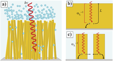 |
| | Fig. 1 (Left) Idealized depiction of a nanowire film functioning as a photoelectrode involved in water splitting. (b, c) Comparison of photogenerated charge carrier collection at (b) planar and (c) high aspect ratio photoelectrodes. The gray bottom represents the back contact for majority carrier collection. | |
The main premise behind Fig. 1 is that a properly designed semiconductor photoelectrode with a high aspect ratio morphology can overcome the constraint that the charge transport properties within the semiconductor match or exceed the light absorption length scales set by the optical properties of the semiconductor in the solar spectrum (Fig. 1b and 1c). In technical terms, a high aspect ratio design should afford a greater attainable photocurrent density for a given material than a planar form without any change in the bulk optoelectronic properties. In practical terms, a high aspect ratio design should ‘fool’ a low-grade, inexpensive semiconductor material into performing like a high-grade, expensive, and efficient semiconductor material. To this end, the ‘nanostructuring’ approach has been applied to a variety of common and newly-developed semiconductor photoelectrode materials. Table 1 summarizes assorted reports on the synthesis and application of nanostructured small and mid-sized bandgap (< 3.0 eV) semiconductors as photoelectrodes in photoelectrochemical cells. The listings in Table 1 do not include dye-sensitized systems or studies focused on solid-state photovoltaics. Table 1 does represent an overview of the general directions and status of the field of photoelectrochemistry through mid-2011. Some of these studies have focused explicitly on producing fuel-forming systems like water-splitting reactors while others have utilized the favorable aspects of photoelectrochemical contacts (e.g. conformal semiconductor/liquid interface, non-destructive nature, and simpler preparation as compared to solid-state metallurgical junctions) to better understand the operation of the materials as light-harvesting elements. Several high aspect ratio morphologies have been explored, including nanotubes, macroporous and mesoporous films, nanorods, and nanonets, amongst others. Dense films of vertically oriented ‘thin’ (radius < 500 nm) nanowires represent the most investigated high aspect ratio architecture. Existing and continually emerging nanowire fabrication processes6,7 offer the possibility of scalable, bottom-up manufacture. Although micron-sized high aspect ratio Si photoelectrodes have received ample attention,8–12 this article will focus on thin nanowire photoelectrodes for three principal reasons. First, large minority carrier diffusion lengths in excess of 10−6 m are difficult to achieve in the majority of the materials in Table 1. Second, the most scalable material syntheses strategies tend to favor thin nanowires. Third, larger total photoelectrode surface areas increase the possible loading capacity of electrocatalysts per projected area.
Table 1 Summary of Reports on Nanostructured Small and Mid-sized Bandgap Semiconductor Photoelectrodes in Photoelectrochemical Cellsa
| Material |
N
D
b/cm−3 |
Morphologyb (dimensions) |
Redox (catalyst)c |
Electrolyte (Solvent)d |
P
in (source)/mW cm−2 |
J
sc/mA cm−2 |
V
oc/mV |
FF; ηe; QYf; qΦ0 /%; /%; (0–1); /eV |
Ref. |
|
NA signifies that property was not available or determinable from presented data.
Dimensions are given as diameter × length where provided.
Catalyst present on nanostructured material.
Aqueous solution unless otherwise noted.
η = (Jsc × Voc × FF)/Pin.
Quantum yield reported on a scale of 0 to 1 at a potential and wavelength provided in the appropriate study; Jsc is given by the current density at the solution potential set by the redox couple and solvent system.
Value estimated from presented data.
List of abbreviations: AO7: Acid orange 7 molecular dye; aq: Aqueous; n-Bu4NClO4: tetrabutylammonium perchlorate; CNT: Carbon nanotube CoPi: Amorphous cobalt/phosphate catalyst; DEA: diethylamine; dmFc: dimethylferrocene; dmFc+: dimethylferrocenium; DMPII: 1,2-dimethyl-3-propylimidazolium iodide; EMISCN: 1-ethyl-3-methylimidazolium thiocyanate; etCO3: Ethylene carbonate; Fc: ferrocene; Fc+: ferrocenium; KHP: Potassium hydrogen phthalate; MV: Methyl viologen; MW: Microwire; NN: Nanonet; NP: Nanoparticle; NR: Nanorod; NT: Nanotube; NW: Nanowire; QE: Quantum efficiency; pCO3: Propylene carbonate; PMII: 1-propyl-3-methylimidazolium iodide; Ppy: polypyrrole; SCCNT: Stacked-cup carbon nanotube; UV: Ultraviolet.
|
|
Group
IV
|
|
n-Si
|
1.1 × 10¹⁵–2.3 × 10¹⁵ |
NW (1.5 μm × 16 μm) |
Br
−/Br2 (Pt) |
40% HBr, 3% Br2 |
100 (solar simulator) |
20.5 |
533g |
43; 4.7; NA; NA |
76
|
|
n-Si
|
3.4 × 10¹⁴–6.4 × 10¹⁴ |
NW (20–300 nm × 15 μm) |
Br
−/Br2 |
40% HBr, 3% Br2 |
100 (AM1.5G) |
1.36 |
730 ± 20 |
45; 0.45; NA; NA |
77
|
|
n-Si
|
1.1 × 10¹⁵–2.3 × 10¹⁵ |
NW (20–300 nm × 17 μm) |
Br
−/Br2 (Pt) |
8.6 M HBr, 0.05 M Br2 |
100 (solar simulator) |
17.2 |
550 |
61; 8.14; NA; NA |
78
|
|
n-Si
|
4.8 × 10¹⁵ |
Macroporous (0.5–3 μm features) |
Br
−/Br2 (Pt) |
8.6 M HBr, 0.05 Br2 |
100 (AM1.5G) |
31.6 |
595 |
70.6g; 13.3; NA; NA |
59
|
|
n-Si
|
4.8 × 10¹⁵ |
Macroporous (<0.5–3 μm features) |
Br
−/Br2 (Pt) |
8.6 M HBr, 0.05 Br2 |
100 (AM1.5G) |
33.2 |
570 |
65.0g; 12.3; NA; NA |
79
|
|
n-Si
|
2.92 × 10¹⁴–4.91 × 10¹⁴ |
NW (100–160 nm × 30 μm) |
[Fe(CN)6]3−/4− |
0.5 M KNO3, 0.1 M K3Fe(CN)6, 0.1 M K4Fe(CN)6 |
40 (200 W tungsten halogen lamp) |
0.89 ± 0.05 |
323 ± 10 |
41 ± 6; 0.3 ± 0.06; NA; NA |
60
|
|
n-Si
|
2.92 × 10¹⁴–4.91 × 10¹⁴ |
NW (100–160 nm × 30 μm) |
[Fe(CN)6]3−/4− |
0.5 M KNO3, 0.1 M K3Fe(CN)6, 0.1 M K4Fe(CN)6 |
40 (200 W tungsten halogen lamp) |
0.89 |
323 |
41; 0.3 ± 0.06; NA; NA |
80
|
|
n-Si
|
4.58 × 10¹⁵–5.11 × 10¹⁵ |
Macroporous (∼1 μm diameter pores) |
Br
−/Br2 (Pt) |
8.6 M HBr, 0.05 M Br2 |
100 (AM1.5G) |
28.4–36.1 |
503–580 |
56.5–73.0; 10.3–14; NA; NA |
75
|
|
n-Si
|
7.8 × 10¹⁷ |
NW (50–100 nm × 15 μm) |
dmFc+/0 |
0.1995 M dmFc, 0.0005 M dmFc+, 1 M LiClO4 (CH3CN) |
60 (300 W ELH lamp) |
26 ± 1 |
537 ± 26 |
NA; NA; NA; 1 |
39
|
|
n-Si
|
1.0 × 10¹⁵–4.8 × 10¹⁵ |
NW (100 nm × 20 μm) |
I−/I3− (Pt) |
0.05 M I2, 0.1 M LiI (PMII/EMISCN) (13![[thin space (1/6-em)]](https://www.rsc.org/images/entities/char_2009.gif) :7) :7) |
50 (AM1.5) |
23.2 |
322 |
40; 6.0; NA; NA |
81
|
|
n-Si
|
4.4 × 10¹⁴–7.1 × 10¹⁵ (P doped) |
Macroporous (∼2–3 μm pore diameter, ∼12 μm pore depth) |
dmFc+/0 |
1 M LiClO4, 0.2 M dmFc, 0.0001 M dmFc+ (CH3OH) |
100 (AM1.5) |
30.6 ± 1.7 |
552 ± 3 |
NA; 46.0 ± 1.6; 0.077 ± 0.003; 1 |
82
|
|
n-Si
|
2.5 × 10¹⁶ |
NW (∼1.5 μm × 10–30 μm) |
dmFc+/0 |
0.2 M dmFc, 0.0005 M, dmFcBF4, 1 M LiClO4 (CH3OH) |
100 (300 W ELH) |
1.43 ± 0.14 |
389 ± 18 |
NA; NA; NA; NA |
83
|
|
n-Si
|
1.1 × 10¹⁵–1.7 × 10¹⁵ |
NW (∼250 nm × 12.25 μm)g |
dmFc+/0 |
1 M LiClO4, 0.2 M dmFc 0.0001 M dmFcBF4 |
100 (AM1.5) |
31 |
550 |
59; 10.1; NA; NA |
84
|
|
n-Si
|
1018 |
NW (200 nm × 18 μm) |
dmFc+/0 |
1 M LiClO4 0.2 M dmFc, 0.0005 M dmFcBF4 |
100 (AM1.5) |
4.19 ± 0.60 |
324 ± 50 |
NA; NA; NA; NA |
41
|
|
n-Si/CNT |
1.1 × 10¹⁵–2.3 × 10¹⁵ |
NW (90 nm × 135 μm) |
Br
−/Br2 |
40% HBr, 3% Br2 |
100 (AM1.5G) |
20.8 |
520 |
41.1; 4.44; NA; NA |
85
|
|
p-Si
|
1017 |
NW (1.5 μm × 100 μm) |
MV2+/+ |
0.05 M MV2+, 0.003 M MV+, 0.5 M K2SO4 |
20 (808 nm) |
4.6 ± 0.7 |
356 ± 21 |
26 ± 3; 3.1 ± 0.8; NA; NA |
86
|
|
p-Si
|
NA
|
NW (57 ± 12 nm × 14 μm) |
Ru(bpy)32+/+/0/− |
NA
|
840 (Hg/Xe arc lamp) |
NA
|
220 |
NA; NA; NA; NA |
87
|
|
p-Si
|
2.2 × 10¹⁶ |
NW (1.6 μm × 100 μm) |
MV2+/+ |
0.5 M K2SO4, 0.047 M MV2+, 0.003 M MV+, 0.1 M KHP H2SO4 (pH = 2.9) |
60 (808 nm) |
7.7 ± 0.9 |
410 ± 40 |
50 ± 5; 2.6 ± 0.4; 0.20 ± 0.02 (808 nm); NA |
11
|
|
III–V
|
|
p-InP
|
NA
|
NW (50–90 nm × 1.5 μm) |
MV2+/+ |
0.001 MV(PF6)2, 0.1 M n-Bu4NClO4 (CH3CN) |
840 (AM1.5) |
NA
|
100 |
NA; NA; NA; NA |
88
|
|
n-InP
|
2–3 × 10¹⁸ |
Macroporous (130 nm diameter, 9,6 μm pore depth) |
[Fe(CN)6]3−/4− |
0.001 M K3Fe(CN)6 |
NA (tungsten lamp) |
0.48 |
800 |
NA; NA; NA; NA |
89
|
|
p-GaP
|
3.98 × 10¹⁷ |
Macroporous (2 μm diameter pores) |
H+/H2 |
1 M H2SO4 |
100 (white light) |
0.057g |
350g |
NA; NA; 0.043 (350 nm)g; 0.92 ± 0.04 |
90
|
|
n-GaP
|
5 × 10¹⁷ |
Macroporous (45.4 μm pore depth) |
Fc/Fc+ |
1 M LiClO4, 0.02 M Fc, 0.0005 M Fc+ |
100 (ELH lamp) |
2.12 |
1060 |
68; 1.5; 1.12 (330)g; 1.6 |
58
|
|
II–VI
|
|
CdSe
|
NA
|
NW (30–40 nm × < 5 μm) |
S/S2− |
(polysulfide) |
80 (1kW Xenon) |
10.11 |
390 |
41; 2.01; NA; NA |
91
|
|
CdSe
|
NA
|
NT (41.9 nm diameter, 10 nm wall thickness) |
S/S2− |
0.2 M Na2S, 0.2 M S, 0.2 M NaOH |
80 (AM1.5G) |
3.52 |
308 |
40.1; 0.57; NA; NA |
92
|
|
CdSe
|
NA
|
NW (10–15 nm × 15 μm) with quantum dots |
S/S2− |
0.05 M Na2S |
330 (tungsten-halogen lamp) |
0.08g |
540g |
NA; NA; 0.25 (500 nm); NA |
93
|
| n-CdS |
NA
|
NW (50–150 nm × ∼1–5 μm) |
S/S2− |
1 M NaOH, 1M Na2S, 1 M S |
100 (NA) |
0.11g |
250g |
NA; NA; NA; NA |
94
|
| CdS |
NA
|
NW (100 nm diameter) |
S/S2− |
0.1 M Na2S, 0.1 M NaOH, 0.1 M S |
35 (NA) |
0.51g |
934g |
45.7; 1.36; NA; NA |
62
|
| CdS/Ppy |
NA
|
NW (<300 nm × < 3 μm) |
S/S2− |
0.1 M Na2S, 0.1 M NaOH, 0.1 M S |
35 (NA) |
1.59g |
133g |
21.9; 5.00; NA; NA |
62
|
|
CdSe on TiO2 |
NA
|
NW (40–60 nm × 100–150 nm) |
S/S2− |
0.2 M NaOH, 0.2 M Na2S, 0.2 M S |
100 (white light) |
0.2 |
340 |
57; NA; 0.028 (500 nm); NA |
95
|
|
CdSe
|
NA
|
NW (30 nm diameter) |
S22−/S2− |
0.1 M polysulfide |
80 (NA) |
1.51 |
500 |
20; 0.17; NA; NA |
96
|
| CdS |
NA
|
Microrods (500 nm × 5 μm) |
S22−/S2−SO42−/SO32− |
1 M Na2S, 0.5 NaSO3 |
100 (AM1.5) |
5g |
660g |
NA; 4.3; NA; NA |
97
|
|
n-Cd(Se,Te)
|
1015 |
NW (200 nm × 3.5–7 μm) |
S22−/S2− |
1 M Na2S, 1 M S, 1 M NaOH |
100 (AM1.5) |
5.6 ± 1.2 |
260 ± 27 |
43.3 ± 5.5; 0.62 ± 0.19; NA; NA |
61
|
|
III–VI
|
|
n-In2S3 |
NA
|
Macroporous (≤ 300 nm pores, ∼30 nm wall thickness) |
O2/H2O |
0.01 M Na2S2O3 |
100 (1450 W Xe lamp) |
NA
|
800g |
NA; NA; NA; NA |
98
|
|
V–VI
|
|
Bi2S3 |
NA
|
NT (40 nm × 1–2 μm) |
O2/H2O |
1 M Na2SO3 |
100 (halogen lamp) |
>3g |
800g |
NA; NA; NA; NA |
99
|
|
I–III–V
|
|
p-CuInS2 |
NA
|
NT (70–100 nm × 2.8 μm) |
NA
|
0.5 M Na2S, 0.125 M S, 0.1 M KCl (CH3OH:H2O) (3:2) |
100 (AM1.5) |
5.52 |
330 |
0.26; 0.47; NA; NA |
100
|
|
I–II–IV–VI
|
|
Cu2ZnSnS4 |
NA
|
Macroporous (∼500 nm features) |
H+/H2 (Pt, CdSe) |
0.1 M Na2SO4 NaOH (pH = 9.5) |
NA (300 W Xe, 420–800 nm) |
3g |
450 |
NA; NA; 0.114 (480 nm); NA |
101
|
|
Oxide
|
|
Fe2O3 |
NA
|
Macroporous (115 nm pore diameter, 400 nm pore depth) |
O2/H2O |
0.5 M H2O2, 1 M NaOH |
100 (AM1.5) |
0.4g |
620g |
NA; NA; NA; NA |
48
|
|
α-Fe2O3 |
NA
|
NW (∼200 nm × 10 μm) |
O2/H2O |
1 M NaOH |
100 (AM1.5) |
< 0.1g |
< 20g |
NA; NA; NA; NA |
102
|
|
α-Fe2O3 |
(Ti doped) |
Macroporous (80–120 nm features) |
O2/H2O |
1 M NaOH |
100 (AM1.5G) |
0.9g |
300g |
NA; NA; 0.24 (350 nm); NA |
103
|
|
α-Fe2O3 |
6 × 10²⁰ (Si doped) |
Cauliflower-like (10–200 nm features) |
O2/H2O |
1 M NaOH |
100 (AM1.5G) |
1.75g |
320g |
NA; NA; 0.39 (350 nm); NA |
72
|
|
α-Fe2O3 |
NA
|
Columnar mesoporous (∼10–30 nm features, 180 nm film thickness) |
O2/H2O |
1 M KOH |
130 (150 W Xe lamp) |
0.8g |
280g |
NA; NA; 0.158 (350 nm)g; NA |
104
|
|
α-Fe2O3 |
(4% Pt) |
NW (∼250 nm × 15 μm) |
O2/H2O |
1 M NaOH |
100 (AM1.5) |
5.5g |
450g |
NA; 5; NA; NA |
105
|
|
α-Fe2O3 |
NA
|
NT (50–55nm × 3.77 μm) |
O2/H2O |
1 M KOH |
87 (AM1.5) |
0.8g |
450g |
NA; 0.84; NA; NA |
106
|
|
α-Fe2O3 |
NA
|
NR (50nm × 700nm) |
I−/I3− |
0.5 M I−, 0.5 mM I2 (etCO3/pCO3) (50/50) |
25 (NA) |
NA
|
NA
|
NA; NA; 0.20 (350 nm); NA |
38
|
|
α-Fe2O3 |
(Sn, Pt doped) |
Mesoporous (∼75 nm features, 500 nm film thickness) |
O2/H2O |
1 M NaOH |
100 (AM1.5) |
0.56 |
300 |
NA; NA; NA; NA |
107
|
|
α-Fe2O3 |
NA
|
NT (78–144 nm × 1.5 μm, 12–22 nm wall thickness) |
O2/H2O |
1 M KOH |
NA (300 W, AM1.5) |
0.94g |
500g |
NA; NA; NA; NA |
108
|
|
α-Fe2O3 |
NA
|
NT (55 nm × 3 μm) |
O2/H2O |
1 M NaOH |
NA (300 W Xe lamp) |
NA
|
NA
|
NA; NA; 0.035 (380 nm); NA |
109
|
|
α-Fe2O3 |
NA
|
NR (50 nm × 500 nm) |
I−/I3− |
0.5 M LiI, 0.5 mM I2 (etCO3/pCO3) (50/50) |
30 (simulated solar) |
0.16 |
260 |
35; 0.05; NA; NA |
54
|
|
α-Fe2O3 |
(Si doped) |
Cauliflower-like (20–200 nm features, 700 nm film thickness) |
O2/H2O (IrO2) |
1 M NaOH |
100 (AM1.5G) |
3.01 |
400 |
NA; NA; >0.5 (320 nm); NA |
110
|
|
α-Fe2O3/TiSi2 |
NA
|
NN (100nm × 500nm) |
O2/H2O |
1M NaOH |
100 (AM1.5) |
0.55g |
400g |
NA; NA; 0.46 (400 nm); NA |
111
|
|
WO3 |
NA
|
Mesoporous (50–100 nm features, 2.5 μm film thickness) |
O2/H2O |
1 M HClO4 |
NA (150 W Xe lamp, AM1.5) |
1.7g |
>750g |
NA; NA; 1.90 (400 nm)g; NA (QY w/0.1 M CH3OH) |
112
|
|
WO3 |
NA
|
Mesoporous (∼50 nm features, 0.4 μm film thickness) |
O2/H2O |
3 M H2SO4 |
NA (AM1.5) |
1.65g |
700g |
NA; NA; 0.42 (290 nm); NA |
113
|
|
WO3 |
NA
|
Macroporous (80 nm pore diameter, 10–15 nm wall thickness) |
O2/H2O |
0.5 M Na2SO4 |
100 (Xe lamp) |
0.2g |
400g |
NA; NA; NA; NA |
114
|
|
WO3 |
NA
|
NW (100–500 nm × 5 μm) |
O2/H2O |
0.5 M H2SO4 |
1.5 (300 W Hg lamp) |
0.54g |
∼1000g |
NA; 13.5; NA; NA |
115
|
|
WO3 |
NA
|
Mesoporous (50–100 nm features) |
O2/H2O |
0.5 M Na2SO4 |
NA (150 W Xe lamp) |
2.1g |
500g |
NA; NA; NA; NA |
116
|
|
WO3 |
NA
|
Mesoporous (70–90 nm features) |
O2/H2O |
0.5 M H2SO4 |
100 (Xe lamp) (< 400 nm light filtered) |
2.1g |
800g |
NA; 0.91; NA; NA |
117
|
|
WO3 |
NA
|
NW (tapered from 100 nm [base] to 30 nm [tip] × 500–1500 nm) |
O2/H2O |
0.1 M Na2SO4 |
100 (AM1.5) (<400 nm light filtered) |
> 0.5 |
> 300 |
NA; NA; 0.24 (350 nm); NA |
118
|
|
WO3 |
NA
|
Nanoflakes (20–30 nm thick, 5–6 μm high) |
O2/H2O |
0.1 M Na2SO4 |
100 (AM1.5) (<400 nm light filtered) |
> 0.5 |
> 300 |
NA; NA; 0.70 (350 nm); NA |
118
|
|
WO3 |
NA
|
Mesoporous (10–40 nm pore width, 2.5 μm film thickness) |
O2/H2O |
0.1 M CH3OH, 1 M HClO4 |
0.049 (420 nm) |
3.25g |
630g |
NA; NA; 1.675 (420 nm); NA |
119
|
|
WO3 |
1018 |
Porous (10 nm wall thickness, 280 nm film thickness) |
O2/H2O |
0.1 M H2SO4 |
NA (350 nm) |
NA
|
600g |
NA; NA; NA; NA |
120
|
|
WO3 |
NA
|
Nanoporous (5–15 nm features) |
O2/H2O |
0.5 M Na2SO4, 0.1 M HCOONa |
NA (150 W Xe lamp) |
4.2g |
600g |
NA; NA; 1.80 (320 nm); NA |
121
|
|
p-Cu2O
|
NA
|
NW (300–400 × 5–10 μm) |
H+/H2 |
0.5 M Na2SO4 |
100 (AM1.5G) |
> 0.7g |
460g |
NA; NA; NA; NA |
122
|
|
p-Cu2O
|
NA
|
Macroporous (340 nm pores, 40 nm wall thickness) |
H+/H2 |
0.5 M Na2SO4 |
NA (He–Cd laser, 441.6 nm) |
0.1g |
> 650g |
NA; NA; NA; NA |
123
|
|
CeO2 |
NA
|
NR (200nm × 7.2 um) |
CH3O•/CH3OH |
1 M KOH, 1 M CH3OH |
NA (500 W Xe lamp, ≥ 390 nm) |
NA
|
NA
|
NA; NA; NA; NA |
124
|
| W0.3Ti0.3 O2/TiSi2 |
NA
|
NN (100nm × 1 μm) |
O2/H2O |
0.05 M KOH |
100 (AM1.5) |
≥ 1g |
780g |
NA; 0.83; NA; NA |
125
|
|
Bi12TiO20 |
NA
|
NW (90nm × 90nm × 200nm) |
O2/H2O |
1 M KOH |
90 (solar simulator) |
2.4g |
1000g |
NA; NA; NA; NA |
126
|
| TixFeyO |
(6.6% Fe) |
NT (75nm × 1500nm, 22 nm wall thickness) |
O2/H2O |
1 M NaOH |
100 (AM1.5) |
0.22g |
> 200g |
NA; NA; NA; NA |
127
|
|
p-CuxTiyO
|
NA
|
NT (65 nm × 1 μm, 35 nm wall thickness) |
H+/H2 |
(CH3OH/H2O/DEA) (5:5:2) |
100 (AM1.5) |
0.06 |
100g |
NA; NA; NA; NA |
128
|
|
BiVO4 |
NA
|
Nanowall (15 nm wall thickness, ∼200 nm pores) |
O2/H2O |
0.5 M Na2SO4 |
158 (470 nm LED) |
0.05g |
600g |
NA; NA; NA; NA |
129
|
|
BiVO4 |
NA
|
Nanopyramids (500 nm base, 25 nm tip) |
O2/H2O |
0.5 M Na2SO4 |
100 (AM1.5) |
0.24g |
1000g |
NA; NA; NA; NA |
130
|
|
CuWOx |
NA
|
NW (∼3 nm length) |
H+/H2 |
0.001 M NaOH |
125 (tungsten halogen lamp) |
NA
|
800g |
NA; NA; NA; NA |
131
|
| n-TixNbyZrzO |
NA
|
NT (10 ± 2 nm × 4 or 7 nm) |
O2/H2O |
1 M KOH |
100 (320–400 nm UV) |
26g |
1000 |
NA; 11.4; NA; NA |
132
|
|
Nitride
|
|
|
|
|
|
|
|
|
|
|
n-WN2 |
NA
|
NW (40–70 nm × 2–3 μm) |
O2/H2O |
0.5 M H2SO4 |
100 (AM1.5) |
1.2g |
920g |
NA; 0.4; NA; NA |
133
|
|
Ta3N5 |
NA
|
NT (45 nm × 6 μm) |
O2/H2O |
1 M KOH |
NA (AM1.5) |
NA
|
NA
|
NA; NA; 0.053 (450 nm); NA |
134
|
|
Oxynitride
|
|
TaON
|
NA
|
NT (60 ± 5 nm × 525 nm) |
O2/H2O |
1 M KOH |
87 (AM1.5) |
2.0g |
1000g |
NA; NA; NA; NA |
135
|
|
Blends
|
|
CdS-Bi2S3 (1:1) |
1.2 × 10²⁰ |
Nanowires (50 nm diameter) |
S/S2− |
0.5 M Na2Sx |
50 (tungsten lamp) |
< 0.5g |
∼100g |
16.82; 0.36; NA; NA |
136
|
|
CdS-Bi2S3 (1:5) |
3.0 × 10²⁰ |
Mesoporous (30–50 nm “walls”) |
S/S2− |
0.5 M Na2Sx |
50 (tungsten lamp) |
< 0.5g |
∼100g |
17.36; 0.96; NA; NA |
136
|
Irrespective of the specific redox system, the cumulative results in Table 1 are encouraging. Many materials long thought impractical for solar energy conversion have demonstrated promising photoelectrochemical responses. Still, Table 1 illustrates that a tenable system or clear set of material options that enable high efficiency solar energy conversion have yet to be recognized. The net energy conversion efficiency for any photoelectrochemical system, ηPEC, can be understood through eqn (1),
| | | ηPEC = ηoptical×ηseparation×ηechem | (1) |
where
ηoptical,
ηseparation, and
ηechem are the system efficiencies for light absorption, charge carrier separation within the semiconductor and transport to the semiconductor/electrolyte interface, and the associated electrochemical transformation, respectively. For any complete system analysis of
ηPEC, all three system contributions must be rigorously assessed. The optical properties of nanostructured semiconductor materials in the context of light collection
13–17 and the electrocatalysis of
fuel-forming redox transformations
18–21 have been reviewed extensively and are outside the scope of this work. This article provides a quantitative framework to understand how to design nanostructured photoelectrodes with optimal
ηseparation.
Scope
The scope of this perspective article is specifically to identify and to define more precisely the limiting factors in the operation of thin nanowire photoelectrodes to aid in their experimental design, synthesis, and implementation. In this work, we set out to describe the typical operation of a thin nanowire photoelectrode operating under low-level injection conditions, i.e. illumination levels where the concentration of only one charge carrier type changes appreciably. Fig. 2 illustrates the relevant charge carrier processes in a thin nanowire photoelectrode in contact with an electrolyte containing the redox couple A/A−. The four processes outlined in Fig. 2 are expected to be the primary processes of importance under low-level injection.22 Additional recombination pathways including radiative recombination and Auger recombination are not significant for indirect bandgap semiconductors like Si and GaP photoelectrodes under low-level injection.22,23 Previous experimental reports on highly doped semiconductor photoelectrodes have shown that tunneling processes such as thermally enhanced field emission and indirect, multistep tunneling are also not significant recombination pathways at the doping concentrations considered here,24 presumably due to the low (relative to metal contacts in traditional Schottky junctions) density of acceptor states in solution.25 For the purposes of this analysis, it is important to recognize that processes 1–4 in Fig. 2 constitute the factors that determine the current in a nanowire in the absence of illumination, i.e. the ‘dark’ current. The dark current in a semiconductor photoelectrode often takes the form of eqn (2),where J0 is the exchange current density at zero bias and f(V) is typically an exponential function of the applied bias. Under illumination, the net current, Jnet, at any potential is then given by eqn (3),| | | Jnet = J0 × f(V) − Jph | (3) |
where Jph is the photocurrent induced by illumination and the negative sign indicates that only Jph contributes to optical energy conversion. At open-circuit conditions under illumination where Jnet = 0, the maximum electromotive force, Voc, that a semiconductor photoelectrode can supply to drive electrochemical reactions in solution often takes the form of eqn (4).22| |  | (4) |
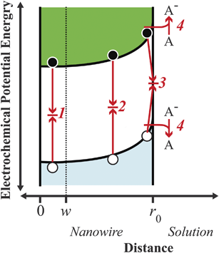 |
| | Fig. 2 Energy band diagram illustrating the four principal processes relevant in a cylindrical nanowire photoelectrode under low-level injection: charge carrier recombination (1) in the bulk, (2) in the depletion region, (3) at surface traps, and (4) through heterogeneous charge transfer. The point w is defined as the edge of the depletion region, i.e. the innermost position over which an appreciable internal electric field is dropped. Filled black circles and empty white circles denote photoexcited electrons and holes, respectively. | |
Hence, an analysis of the factors that determine the magnitude of J0 is necessary to appreciate and interpret the operation of a thin nanowire photoelectrode.
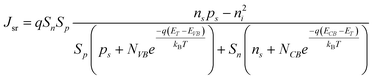
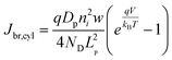
Processes labeled 3 and 4 in Fig. 2 describe parallel charge carrier recombination pathways at the surface of a semiconductor photoelectrode. Eqns (5) and (6) express the rate of each process as a current density. The specific terms in eqns (5) and (6) are defined and summarized in Table 2. Eqn (5) represents the analytic expression for the ‘dark’ current at a semiconductor photoelectrode under the limiting condition of surface recombination (process 3 in Fig. 2).22
| |  | (5) |
Table 2 Description of terms
| Symbol |
Description |
Symbol |
Description |
Symbol |
Description |
|
q
|
unsigned charge of electron |
D
n
|
electron diffusion constant |
E
T
|
energy of trap states |
|
k
B
|
Boltzmann's constant |
D
p
|
hole diffusion constant |
E
CB
|
conduction band edge |
|
T
|
temperature |
L
n
|
electron diffusion length |
E
VB
|
valence band edge |
| [A] |
concentration of acceptors in electrolyte |
L
p
|
hole diffusion length |
N
CB
|
effective density of states in the conduction band |
| [A−] |
concentration of donors in electrolyte |
τ
n
|
electron lifetime |
N
VB
|
effective density of states in the valence band |
|
n
i
|
intrinsic carrier concentration |
τ
p
|
hole lifetime |
N
D
|
dopant concentration |
|
n
s
|
surface electron concentration |
Z(r0,w)
|
effective recombination area as defined by explicit integral over w and r0 (see ESI) |
k
et
|
electron charge transfer constant |
|
p
s
|
surface hole concentration |
r
dr,max
|
radial position of maximum recombination rate in the depletion region |
k
ht
|
hole charge transfer constant |
|
n
s0
|
surface electron concentration in the dark at equilibrium |
S
n
|
electron surface recombination velocity |
Φ
0
|
interfacial equilibrium barrier height |
|
p
s0
|
surface hole concentration in the dark at equilibrium |
S
p
|
hole surface recombination velocity |
B
0, B1 |
Zero-order and first-order Bessel functions of the first kind, respectively |
In eqn (5), the potential dependence of Jsr arises from ns and ps which are the potential-dependent concentrations of electrons and holes, respectively, at the surface. Similarly, eqn (6) describes charge carrier recombination of electrons and holes at the surface through heterogeneous charge transfer.2,26,27
| | | Jct = qket[A](ns − ns0) − qkht[A−](ps − ps0) | (6) |
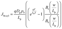
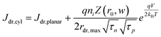
In eqn (6), the potential dependence of Jct arises from ns and ps. For an n-type photoelectrode, eqn (6) illustrates that higher concentrations of electrons at the surface will deleteriously increase the magnitude of the dark current. The expressions for Jsr and Jct apply to all photoelectrode morphologies and are not unique to thin nanowire photoelectrodes. Conversely, processes 1 and 2 in Fig. 2 represent recombination pathways that are geometry dependent, i.e. the analytical expressions for these processes are not equivalent to planar and high aspect ratio thin nanowire photoelectrodes. The analytical expressions describing charge carrier recombination in the bulk and in the depletion region of a thin cylindrical nanowire photoelectrode are derived from the flux conditions in cylindrical coordinates, which differ from the simple 1D coordinate system used for planar photoelectrodes. The explicit equations that separately express the rates of charge carrier recombination in the bulk and in the depletion region for planar photoelectrodes have been summarized previously.22Eqn (7a) details the rate of bulk recombination expressed as a current density inside a thin cylindrical n-type nanowire. When the minority carrier diffusion length for a thin cylindrical n-type nanowire is much larger than the field-free region, the expression for the rate of bulk recombination as a current density simplifies to eqn (7b).
| |  | (7a) |
| |  | (7b) |
The derivation of eqn (7) is presented in the ESI.†Eqn (8a) describes charge carrier recombination in the depletion region within a thin cylindrical semiconductor.
| |  | (8a) |
| | 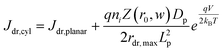 | (8b) |
Eqn (8a) is the general expression where no assumption is made regarding the respective lifetimes for electrons and holes. For bulk recombination described by the Shockley-Read-Hall formalism
22,23 with equal electron and hole trap capture cross sections and trap densities, the carrier lifetimes are equivalent and the depletion region recombination rate as a current density can be described by
eqn (8b). The derivation of
eqns (8a) and (8b) is given in the ESI.
† For thin
nanowires, the second term on the right hand sides of
eqns (8a) and (8b) becomes significant. The descriptions of the specific terms in
eqns (7) and
(8) are also summarized in
Table 2. In a real thin
nanowire photoelectrode, the solar energy conversion properties can be dictated by any individual, combination, or sum total of the processes 1–4 in
Fig. 2. It is difficult to predict
a priori which, if any, of
eqn (5)–(8), properly describe
J0 in a particular system at every experimentally relevant condition.
Since insight on the controlling factors of a thin semiconductor nanowire photoelectrode would be extremely useful for guiding and improving the efficacy of experimental efforts aimed at increasing ηseparation (and ηPEC accordingly), a quantitative analysis of the operation of thin nanowire photoelectrodes through a set of two-dimensional, finite-element simulations has been undertaken. Such approaches have previously been used to separately model planar semiconductor photoelectrodes in photoelectrochemical systems28 and solid-state cylindrical p–n nanowire homojunctions.29–31 Herein, we report modeling efforts explicitly aimed at describing the operation of thin Si and GaP nanowire photoelectrochemical heterojunctions. Si and GaP represent small and mid-sized bandgap semiconductors previously investigated as photoelectrode materials for artificial photosynthesis.32 The optical and electronic properties of these two materials have also been extensively detailed in the literature, facilitating the present analyses. The purpose of these studies is to provide a quantitative basis for identifying the controlling factors in thin nanowire photoelectrodes so as to define and to prioritize experimental strategies for improving solar energy conversion efficiency. Results are first presented that describe the extent to which majority carrier recombination at the front contact though heterogeneous charge transfer is sensitive towards non-uniform dopant concentrations and nanowire shape. Separately, an examination of how variations in the nanowire radius, surface recombination velocity, charge carrier mobilities, and charge carrier lifetimes affect the photocurrent-potential response is presented. Finally, simulations intended to explore the possibility of thin nanowire photoelectrodes operating under high-level injection conditions are discussed.
Method
A simulation software package (Sentaurus Device, Synopsys) featuring the finite-element box method33 was used to model the steady-state operation of ideal and tapered cylindrical photoelectrodes. Sentaurus Device solves Poisson's equation subject to Fick's law of diffusion to approximate diffusion, drift, recombination, and generation in semiconductor devices and has been extensively used for modeling photovoltaic architectures in one, two, and three dimensions.8,34,35 For modeling a three-dimensional cylindrical photoelectrode, a radial coordinate system was employed with structures featuring D∞h symmetry (Fig. 3a) to treat a three-dimensional object using only two spatial coordinates, r and z. A pictorial representation of the meshing design used for the ideal cylindrical nanowire is presented in the ESI.† Unless noted otherwise, each simulation featured an ohmic contact at the base of the nanowire (denoted as the ‘back’ contact). The back contact was modeled as a perfect ohmic contact with S = 107 cm s−1. The side and top of the nanowire (denoted as the ‘front’) were uniformly in contact with a single conductor that effected an interfacial equilibrium barrier height of 1 eV for Si and 2 eV for GaP. To approximate a semiconductor/liquid contact, electron and hole transfer velocities (ket[A] and kht[A−], respectively) of 100 cm s−1 were used throughout unless indicated otherwise. No other physical aspects of the electrolyte (e.g. dielectric constant) were incorporated into the models. These electron and hole carrier velocities are commensurate with known rate constant values for outer-sphere redox couples (10−17 -10−19 cm4 s−1)26,36 at concentrations typical of photoelectrochemical experiments (10−1 to 101 M). For all simulations, bulk and surface recombination were modeled with a single trap level located at the energy of the intrinsic Fermi level approximately in the center of the bandgap (τn = τp = τ; Sn = Sp = S). For simulations involving discrete ohmic-selective contacts, each contact was a thin concentric band located an equal distance from the other ohmic-selective contact and the nearest top/bottom boundary. Unless indicated otherwise, the majority of simulations featured high aspect ratio structures with a vertical height of 100 μm. For a distorted cylindrical nanowire, the radius of the top structure was decreased relative to the radius of the base without adjusting the vertical height, creating a taper (Fig. 3a). All simulations assumed standard pressure and temperature conditions. In each presented dataset, only one or a pair of optoelectronic parameters were varied, with all other aspects of the semiconductor held constant. The variables describing the bulk optoelectronic properties of the semiconductor, the contacting electrolyte, and the associated charge transfer kinetics for each set of simulations are tabulated in the ESI.† A simple Beer–Lambert optical excitation profile was used to simulate the steady-state photogeneration of carriers, with the direction of illumination normal to the top surface plane. In these simulations, the reflectivity of the illuminated interface was set to zero so that the respective fractions of the absorbed and transmitted light summed to one. Unless indicated otherwise, each simulation was performed assuming white light illumination with a spectral profile equivalent to AM 1.5 (direct + circumsolar) illumination. The explicit generation profile used in these simulations is shown in Fig. 3b for AM 1.5 (direct + circumsolar) illumination. For most simulations, the integrated power density of the white light illumination was 100 mW cm−2. For simulations at higher total illumination intensities, the AM 1.5 (direct + circumsolar) spectrum was scaled with a uniform multiplicative factor as indicated. When given, quantum yield values are on a scale from 0 to 1 and represent the ratio of the collected current to the number of absorbed photons per projected area per second. The wavelength-dependent values of α used for each simulation were determined from published optical data for Si and GaP.37,38
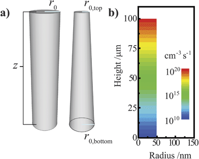 |
| | Fig. 3 (a) Depiction of the (left) cylindrical and (right) tapered cylindrical nanowire models used in this work, with r0 indicating the effective radius. (b) The Beer–Lambert optical generation profile in a cylindrical nanowire under AM 1.5 (direct + circumsolar) illumination at normal incidence used in this work. | |
Results and discussion
Energy conversion losses due to majority
carrier
recombination at the front contact arising from non-uniform dopant concentrations. Extensive carrier recombination losses can occur in nanostructured semiconductor photoelectrodes with inadequate dopant concentrations. We have previously presented analyses on the dependence of the efficiency for photogenerated carrier collection with the dopant concentration in thin nanowire photoelectrodes.39 In that study, two-dimensional modeling results verified the experimental observations that a minimum dopant concentration was necessary to ‘fit’ a sufficiently compact depletion region within the nanowire. At dopant concentrations too low to support a large internal electric field, majority carriers were not preferentially directed away from the front surface and thus could recombine with minority carriers via heterogeneous charge transfer (i.e. process 4 in Fig. 2). If this minimum dopant concentration criterion was not satisfied, majority carrier-based recombination at the front surface substantially increased and resulted in low to no net photogenerated carrier current collection. Although complementary observations on this effect in uniformly-doped semiconductor nanowire heterojunctions have been recently discussed,39–41 the same majority carrier-based heterogeneous charge transfer recombination losses in systems with non-uniform dopant profiles have not been detailed.
Non-uniform doping profiles are common in nanowire systems. For semiconductor nanowires, incorporation of dopants is achieved either during nanowire synthesis42 or via post-synthesis processing. For post-synthesis processing, the dopant can be introduced through means such as diffusion ‘drive-in’ or ion implantation.43 Spatial variation of dopant concentration in thin semiconductor nanowires has been previously studied.42–46 Ion implantation can result in Gaussian-like spatial dopant distributions, but the specific dopant concentration–distance profile is highly dependent on the particular conditions used for implantation.47 By comparison, drive-in diffusion doping with a constant source is a simpler strategy that yields predictable dopant concentration–distance profiles according to eqn (9),
| |  | (9) |
where
C(
r,
t) is the dopant concentration as a function of the radial dimension (
r) and the total time used to drive in the dopant (
t),
Cs is the surface dopant concentration,
erfc(
x) is the complementary error function, and
Ddopant is the diffusion coefficient for a specific dopant in the semiconductor at a particular temperature.
48 In
eqn (9), the term

describes an effective distance from the surface to which the dopant is able to diffuse under the employed doping conditions. The consequences of non-uniform doping profiles in thin
nanowire photoelectrodes rendered by inadequate ‘drive-in’ diffusion doping conditions (temperature and time) are assessed in
Fig. 4.
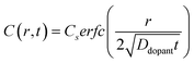
Fig. 4a–c illustrate dopant concentration-radial position profiles according to
eqn (9). In these profiles, the center corresponds to 0 nm and the outer surface edge is at 50 nm. In each profile, the surface dopant concentration was set to 1 × 10
18 cm
−3. The inner edge of the depletion width for a 1 eV interfacial equilibrium barrier height is denoted with a vertical dotted line. These three profiles differ by the level of ‘background’ doping,
i.e. the intrinsic concentration of electrically active dopants. For background doping, three constant values of 1 × 10
16, 1 × 10
17 cm
−3, and 3 × 10
17 cm
−3 (
Fig. 4a, b, and c, respectively) were used which were all too low to completely suppress majority-carrier recombination at the surface under illumination. The four concentration profiles for each ‘background’ doping level correspond to values of

that span three orders of magnitude.
Fig. 4d summarizes the calculated quantum yield at short circuit from 120 separate device simulations for a cylindrical Si
nanowire with
r0 = 50 nm,
z = 100 μm, and an interfacial equilibrium barrier height of 1 eV. The full set of optoelectronic properties used in these simulations is collected in Table S1 in the Supporting Information. For values of

large enough to effect a uniformly high dopant density, the modeled photoresponses showed perfect quantum yields indicating no majority carrier recombination losses. For the smallest values of

, the quantum yield values were much less than unity, in agreement with
nanowire photoelectrodes with insufficient doping levels.
39,41 For intermediate values of

less than 4 × 10
−8 m, the steepness in drop in quantum yield was a function of the ‘background’ doping level. The results in
Fig. 4d show that even if the near-surface region of a thin
nanowire is adequately doped, majority carrier recombination at the surface cannot be entirely suppressed unless the entire depletion region is sufficiently doped to sustain the internal electric field dictated by the interfacial equilibrium barrier height. The data in
Fig. 4d also represent a practical guide for the preparation of thin
nanowires that are resistant against majority carrier recombination. For example, phosphorus is an n-type dopant in Si with a dopant diffusivity of 1.16 × 10
−15 cm
2 s
−1 at
T = 1200 K.
48,49 This analysis indicates that a minimum ‘drive-in’ time of one hour is necessary to reach the minimum requisite value of

at this process temperature. Shorter diffusion times, lower temperatures, or other complications in the doping process will result in nanostructured materials with low or no appreciable photoactivity, irrespective of all other optoelectronic properties of the material.
 |
| | Fig. 4 (a–c) Calculated dopant profiles across the radial dimension of a Si nanowire with a radius of 50 nm following ‘drive-in’ diffusion doping to a level of 1 × 1018 cm−3. Three different background dopant concentrations of (a) 3 × 1017 cm−3, (b) 1 × 1017 cm−3, and (c) 1 × 1016 cm−3 were modeled. In each plot, four different values of 2(Ddopantt)1/2 were used to calculate the dopant profile as described in the text. (d) The calculated internal quantum yield at short-circuit as a function of the calculated dopant profile from the value of 2(Ddopantt)1/2. The illumination conditions of the simulations were λ = 750 nm at 1 × 10¹⁷photons cm−2 s−1. The optoelectronic properties used for the Si nanowire are collected in Table S1. | |
Energy conversion losses due to majority
carrier
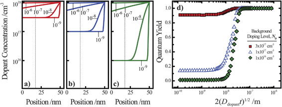
recombination via heterogeneous charge transfer in tapered
nanowire
photoelectrodes. A common observation in the preparation of long nanowires is that their radii are not constant along their entire length, with tapering of the top portion with respect to the base.50–53 For thin nanowire photoelectrodes, sections that are too thin to support the full internal electric field dictated by the interfacial equilibrium contact and doping level will allow substantial majority carrier recombination at the front contact. Simulations were performed with ideal and tapered cylindrical Si nanowires with z = 100 μm, illuminated at AM 1.5 (direct + circumsolar) insolation. The full photocurrent-potential responses are shown in Fig. 5, with the photocurrents normalized by the total absorbed photons and expressed as quantum yields. The five photoelectrode architectures are shown as an inset to Fig. 5. Two thin cylindrical nanowires with r0 = 300 and 50 nm (I and II, respectively) and three tapered cylindrical nanowires with r0,base = 300 nm and r0,top = 150, 100, and 50 nm (III, IV, and V, respectively) with a uniform dopant concentration of 2 × 1016 cm−3 were studied. Since the dopant concentrations were uniform for all investigated nanowires, the observed changes in open-circuit photovoltage were small. The dominant consequence of tapering was a decrease in attainable photocurrent. NanowireI was properly sized to minimize majority carrier recombination through charge transfer at the surface and thus showed unity quantum yield at short circuit. Conversely, nanowireII was too thin for this dopant level and majority carrier recombination through charge transfer at the surface lowered the quantum yields for net photocurrent collection to values near zero. The three tapered nanowiresIII, IV, and V all showed lowered attainable quantum yield values relative to nanowireI. Even with the least tapering, the quantum yield at short circuit for nanowireIII was 10% lower than for nanowireI. NanowireV showed attainable quantum yield values roughly 33% lower than nanowireI. In practice, this photocurrent collection loss will be sensitive towards the precise photogeneration profile within the nanowire. Nevertheless, the data in Fig. 5 indicate that substantial losses in net photocurrent can arise from physical variation in the shape of the nanowire photoelectrode, irrespective of all other optoelectronic properties of the material.
 |
| | Fig. 5 Comparison of the simulated current–voltage photoresponse under AM 1.5 (direct + circumsolar) illumination from five different high aspect ratio morphologies (I–V) all modeled with a uniform dopant density of 2 × 1016 cm−3 and an interfacial equilibrium barrier height of 1 eV. For I, r0 = 300 nm. For II, r0 = 50 nm. For III, IV, and V, r0,bottom = 300 nm and r0,top = 150, 100, and 50 nm, respectively. The full set of optoelectronic values used in these simulations is collected in Table S2. | |
Energy conversion losses due to charge
carrier
recombination within thin
Si
and
GaP
nanowires
For properly doped, thin nanowire photoelectrodes with trap states located uniformly throughout the material and minimal surface defects, the dominant recombination process could be located in the electric field-free ‘bulk’ (i.e. the volume defined by r = 0 and r = w) or in the depletion region (i.e. the volume defined by r = w and r = r0). As shown in eqns (7) and (8), these two processes have different functional forms with respect to the most direct metric of semiconductor ‘quality,’ i.e. the minority carrier diffusion length. If ‘bulk’ recombination processes are the dominant factor in J0, eqns (7) and (4) predict the attainable open-circuit photovoltage increases 0.12 V per decade increase in Lp in an n-type nanowire. Similarly, if depletion region recombination processes are the dominant factor in J0, eqns (8) and (4) predict an increase in the attainable open-circuit photovoltage of 0.24 V per decade increase in Lp in an n-type nanowire. Since the diffusion length of a charge carrier is a function of both the mobility and lifetime (eqn (10)), we conducted a series of initial simulations to determine the differences in adjusting Lp through changes in either μp, τp or both.
| | 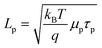 | (10) |
Simulations were performed on thin n-Si cylindrical nanowire photoelectrodes with r0 = 50 nm with a 1 eV interfacial equilibrium barrier height illuminated with AM 1.5 (direct + circumsolar) insolation. For these simulations, total collection of every absorbed photon corresponded to a photocurrent value of 35 mA cm−2. Fig. 6 summarizes the impact on the photocurrent-potential responses from changes in μp and τp, where the value of μp was varied for specific values of τp. In each plot, mobilities larger than the largest mobility value shown effected no further improvement/change in photocurrent–potential profile. The lowest mobility value shown in each plot was two orders of magnitude smaller than either the largest investigated mobility value or the lowest mobility value that allowed self-consistent simulation results. Several general points can be drawn from the data in Fig. 6. First, the specific value for Lp did not intrinsically determine the photoresponse behavior. A minority carrier diffusion length of 5 × 10⁻⁷ m is shown in each plot of Fig. 6 but the photocurrent–potential profiles are decidedly different. Second, the value of τp has a stronger influence on the value of Voc for a thin cylindrical nanowire than μp. Decreasing the lifetime of the minority carrier by two orders of magnitude caused a pronounced diminution in Voc. Conversely, decreasing the mobility of the minority carrier by two orders of magnitude primarily caused a decrease in photocurrent and rectangularity (i.e. the fill factor) of the photocurrent–potential profile. Third, in all scenarios, a comparatively high minority carrier mobility was required to achieve total collection of all absorbed photons in thin cylindrical nanowire photoelectrodes. Specifically, a mobility value on the order of 5 cm2 V−1 s−1 was necessary to ensure complete collection of photogenerated carriers. Based on these findings, we performed further simulations on the dependence of Voc with changes in Lp by setting μp above this threshold value and then adjusting τp. We note that this threshold for carrier mobility is well below the typical carrier mobility values for both crystalline Si and GaP but above that for many mid-sized bandgap metal oxides such as NiO and Fe2O3.54–57
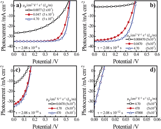 |
| | Fig. 6 Simulated current–voltage photoresponses under AM 1.5 (direct + circumsolar) illumination of a cylindrical n-Si nanowire with a radius of 50 nm and a height of 100 μm in contact with an electrolyte resulting in an interfacial equilibrium barrier height of 1 eV. Several values of μp were assessed at (a) τ = 2.08 × 10⁻⁶ s, (b) τ = 2.08 × 10⁻⁸ s, (c) τ = 2.08 × 10⁻¹⁰ s, and (d) τ = 2.08 × 10⁻¹² s. The full sets of optoelectronic values used in these simulations are collected in Table S3. | |
Fig. 7a and 7c summarize the Voc values recorded for simulations involving thin Si and GaP cylindrical nanowire photoelectrodes, respectively. These nanowire types featured a uniform dopant concentration of 1 × 1018 cm−3 and interfacial equilibrium barrier heights of 1 and 2 eV, respectively. For the n-Si nanowire simulations, the recorded values of Voc were nominally zero and invariant to changes in Lp at exceedingly small values of Lp (< 10−7 m). For values of Lp greater than 10−7 m, Voc increased 0.229 V per decade increase in Lp. For the GaP nanowire simulations, the dependence between Voc and decade changes in Lp was linear for all values of Lp with a slope of 0.232 V per decade. These slopes are noteworthy in three aspects. First, the data in Fig. 6 indicate that large photovoltages are achievable with relatively low-grade mid-bandgap materials like the modeled GaP. This prediction is in accord with recent observations of the photoelectrochemical performance of high aspect ratio GaP photoelectrodes.58 For a thin GaP nanowire with r0 = 500 nm and a minority carrier diffusion length of only 500 nm, a Voc in excess of 1.30 V is attainable under normal solar illumination. Second, a direct comparison of the open-circuit photovoltages between planar and thin nanowire photoelectrodes is not rigorously applicable under all conditions even if the two photoelectrodes have exactly the same optoelectronic properties. The slope values near 0.24 V per decade for the nanowire simulations strongly suggest depletion region recombination as the dominant process in both of these thin nanowire types. Simulations where r0 was varied between 50 nm and 500 nm at a constant value of Lp separately corroborated the predicted dependence of Voc from eqns (4) and (8) when depletion region recombination is the limiting factor (Fig. 7b and 7d). For a planar n-Si photoelectrode with the exact same bulk and (good) surface optoelectronic properties, the Voc-Lp dependence is not limited primarily by depletion region recombination. Instead, bulk recombination controls the value of the open-circuit photovoltage of a planar photoelectrode with a slope of 0.06 V per decade change in Lp (eqn (11); dashed line in Fig. 7a).59
| | 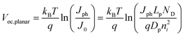 | (11) |
 |
| | Fig. 7 Simulation results under AM 1.5 (direct + circumsolar) illumination for cylindrical (a,b) n-Si and (c,d) n-GaP nanowire photoelectrodes with a radius of 50 nm and a height of 100 μm in contact with an electrolyte resulting in an interfacial equilibrium barrier height of (a and b) 1 eV and (c and d) 2 eV. (a) Analysis of the attainable open-circuit photovoltage with a Si nanowire as a function of the minority carrier diffusion length calculated at two different values of the surface recombination velocity. The dashed line indicates the expected dependence of the open-circuit photovoltage with changes in the minority carrier diffusion length for a comparable planar photoelectrode operating under bulk recombination limitations. (b) Analysis of the attainable open-circuit photovoltage with a Si nanowire as a function of nanowire radius at two different values of the minority carrier diffusion length. (c) Analysis of the attainable open-circuit photovoltage with a GaP nanowire as a function of the minority carrier diffusion length calculated at two different values of the surface recombination velocity. (d) Analysis of the attainable open-circuit photovoltage with a GaP nanowire as a function of nanowire radius at two different values of the minority carrier diffusion length. The complete optoelectronic properties used in the simulations are listed in Tables S4–S7. | |
The consequence of two different processes respectively controlling related planar and thin nanowire photoelectrodes is two different functional forms for J0. Hence, the oft-used ratio of the projected to geometric surface areas as justification for decreased photovoltages in high aspect ratio photoelectrodes is not always applicable.58,60–62 The difference in Voc for the planar and thin nanowire photoelectrodes reflects the fact that charge-carrier generation in the two photoelectrode architectures is different. In a planar photoelectrode, most of the charge-carrier generation in a planar photoelectrode heterojunction occurs far away from the depletion region. In a thin nanowire photoelectrode, the generation of carriers always occurs in or immediately adjacent to the depletion region. The photoresponse behavior of thick nanowires could in principle approach the behavior of planar photoelectrodes, but that was not observed in these studies for Si or GaP nanowires up to r0 = 500 nm. Third, with depletion region recombination as the determining factor for J0, significant increases in attainable solar energy conversion efficiencies of thin nanowire photoelectrodes can be expected through modest increases in the minority carrier diffusion length. Hence, in the design of optimally constructed photoelectrodes, making the magnitude of the minority carrier diffusion length much greater than (rather than just equal to) the radius should be a primary focus.
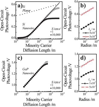
For both Si and GaP nanowire simulation sets, a conversion to bulk recombination as the dominant factor controlling Voc (with an expected slope of 0.12 V per decade change according to eqn (4) and (7)) at large values of Lp was not observed. Instead, Voc became insensitive towards large values of Lp (Fig. 7a and 7c), indicating a switch from depletion region recombination to a surface-specific process with no functional dependence on Lp. The switchover was dependent on the value of S and the discrepancy between the attainable Voc values for large and small values of S were more pronounced for the n–Si nanowire than the n-GaP nanowire models. These simulation results indicated that passivation of surface defects only results in larger open-circuit photovoltages when the bulk quality (i.e. Lp) of the nanowire is sufficiently high. In the absence of sufficiently large Lp values, passivation of surface defects is therefore predicted to have no influence on the attainable photovoltage of a thin nanowire photoelectrode. For short minority carrier diffusion lengths, additional simulations were performed to determine whether S had any effect on the expected photoresponse characteristics of thin nanowire photoelectrodes. Fig. 8 presents three sets of photocurrent-potential responses for models of a planar n–Si, a cylindrical n–Si nanowire, and a cylindrical n-GaP nanowire photoelectrode. For the two n–Si simulation sets, all optoelectronic properties are the same. For the planar n–Si photoelectrode in Fig. 8a, the shape of the photocurrent-potential response was strongly sensitive to the value of S from 1 to 106 cm s−1. Large values of S lowered the overall energy conversion efficiencies through diminution of Voc. By comparison, none of the features of the photoresponses in Fig. 8b of the n-Si cylindrical nanowire photoelectrode showed any sensitivity towards S. Similarly, the photoresponse characteristics of the n-GaP cylindrical nanowire photoelectrode in Fig. 8c were equally invariant towards S. The cumulative data from these simulations argue against the commonly asserted premise that the high surface area of thin nanowire photoelectrodes automatically makes their capacities for solar energy conversion extremely sensitive towards surface defects/traps. The analysis presented here instead supports the contention that under most common configurations, the operation of thin nanowire photoelectrodes is much more strongly sensitive to the bulk optoelectronic properties.
 |
| | Fig. 8 Simulated current–voltage photoresponses under AM 1.5 (direct + circumsolar) illumination of (a) a 100 μm thick planar n-Si photoelectrode, (b) an n-Si nanowire photoelectrode with a radius of 50 nm and a height of 100 μm, and (c) an n-GaP nanowire photoelectrodes with a radius of 50 nm and a height of 100 μm across a range of surface recombination velocity, S, values. The full sets of optoelectronic values used in these simulations are collected in Tables S8 and S9. | |
Solar energy conversion at high-level injection with discrete contacts. The preceding discussion focused exclusively on highly doped thin nanowire photoelectrodes where only the minority carrier concentration changed under illumination. The operation of such high aspect ratio photoelectrodes under high-level injection conditions, i.e. the concentrations of both charge carrier types change substantially under illumination, has yet to be explored. For thin nanowire photoelectrodes to operate under high-level injection conditions, the illumination intensity has to be increased and/or the doping level of the nanowire must be decreased. At first glance, both of these scenarios seem impractical with doped thin nanowire photoelectrodes. In general, the high illumination intensities necessary to push the highly doped thin nanowire photoelectrodes into the high injection level regime will result in an intolerable level of Auger recombination and poor overall optical energy conversion performance.63–65 Separately, decreasing the dopant concentration in thin nanowire photoelectrodes is not favorable for the reasons enumerated above and previously.39 However, those arguments hold rigorously only for doped thin nanowires contacted uniformly by a conductor that effects a large interfacial equilibrium barrier height. If the contacting arrangement is non-uniform, i.e. through discrete contacts for carrier collection,66 the functional forms of eqns (5)–(8) will change and it is not clear a priori how the operation of thin nanowire photoelectrodes will fare.
To assess the possible merit of operating nanowire photoelectrodes in the high-level injection regime, we performed a separate set of simulations that compare the performance of a lightly doped thin nanowire photoelectrode either with a conformal front contact and back contact at the base (as above) or with a pair of discrete, ohmic-selective contacts. White light intensities sufficient to perturb both the concentrations of electrons and holes were used in these simulations and the bulk and surface optoelectronic properties of Si were kept constant between the two device types. Fig. 9a summarizes the modeling results for a lightly doped Si nanowire photoelectrode with a uniform, conformal front contact that produces an interfacial equilibrium barrier height of 1 eV. As expected from the preceding analyses, the overall quantum yields for photogenerated carriers at high-level injection for this device are exceedingly poor and fully consistent with severe majority carrier recombination losses through heterogeneous charge transfer at the surface. As a corollary, the resultant Voc values are also poor even at illumination intensities 1000 times greater than AM 1.5 insolation. Fig. 9b illustrates a simplified model of a thin Si nanowire photoelectrode with discrete ohmic-selective contacts in the form of thin concentric bands. In this structure the exposed surface between the contacts is modeled as a semiconductor/air interface subject to surface recombination at the rate set by S. In this scheme, the bulk of the nanowire is not depleted of carriers and thus is essentially free of any electric field (in contrast to the heterojunction model in Fig. 9a). Fig. 9c summarizes the modeling results of the photocurrent–potential behaviors for one possible design of a discrete contact thin nanowire photoelectrode. The photocurrent–potential responses in Fig. 9c differed significantly from those in Fig. 9a. The quantum yields at short circuit were 70 times greater and the Voc values were more than 0.15 V larger at all investigated illumination intensities. Accordingly, the net energy conversion possible with the discrete contact thin nanowire photoelectrode was approximately two orders of magnitude greater than with the conformal contact thin nanowire photoelectrode.
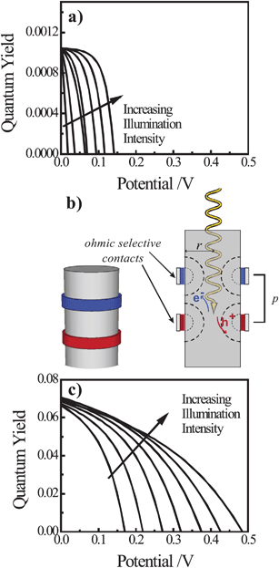 |
| | Fig. 9 (a) Simulated current-voltage photoresponses of a nanowire under white light illumination at 1, 3, 10, 30, 100, 300, and 1000 times AM 1.5 (direct + circumsolar) illumination and featuring a conformal front contact with an interfacial equilibrium barrier height of 1 eV. (b) Schematic depiction of a nanowire photoelectrode with discrete, ohmic-selective contacts. (c) Simulated current–voltage photoresponses of a nanowire with a pair of discrete, ohmic-selective contacts under white light illumination at 1, 3, 10, 30, 100, 300, and 1000 times AM 1.5 (direct + circumsolar) illumination. The full set of optoelectronic values used in these simulations is collected in Table S10. | |
In this preliminary analysis, we have not attempted a thorough investigation of the discrete contact nanowire photoelectrode scheme to determine if Fig. 9c represents or reflects the highest attainable collection efficiencies with this scheme. To be clear, the absolute values of the short-circuit quantum yields in Fig. 9c are too low for practical considerations. However, for perspective, the photoresponses of planar semiconductor photoelectrodes with discrete contacts under high-level injection are strongly dependent on the particular spatial arrangement of contacts and the properties of the semiconductor.66–70 We posit that the same is true in the nanowire case and that a discrete contact configuration with a technologically relevant capacity for energy conversion may yet be possible. A more comprehensive analysis of the limiting processes in nanowires with discrete, ohmic-selective contacts is beyond the scope of this work but should prove valuable. Aside from traditional groupIV and III–V semiconductors, the vast majority of candidate earth-abundant semiconductors for solar energy conversion cannot be easily or precisely doped both n- and p-type. For example, doping strategies even for well-known materials like Fe2O3 are still active areas of research.71–74 Precisely controlling both the morphology and electronic properties of a nanostructured semiconductor photoelectrode could be daunting for many materials and may ultimately be practical only for a select set of semiconductors. However, strategies like the use of discrete contacts, coupled with ohmic-selective contacting materials like conducting polymers,22,75 may be an alternative, general means for utilizing thin semiconductor nanowire materials for solar energy conversion.
Summary and outlook
This analysis focused on the operation of a single nanowire photoelectrode. Notwithstanding differences in the profiles of optical photogeneration of charge, the presented results hold for a photoelectrode composed of a film of nanowires if all of the nanowires have equal size and electrical properties. In practice, low density nanowire arrays with heterogeneity in nanowire size and doping levels are common. Still, in these ensemble systems, the impact of nanowire heterogeneity can be readily understood through the analyses shown here. Variation in the electronic and morphological properties of individual nanowires across a film of thin semiconductor nanowires in the manner described here will unavoidably lower the maximum attainable energy conversion efficiency of the film. To ensure that heterogeneity of nanowire structures in a film does not significantly limit the overall system energy conversion efficiency, methods to rapidly and accurately assess the doping condition in individual nanowires across large areas are vital. Efficient operation of thin nanowire photoelectrodes for solar energy conversion first requires precise control over both the conductive and morphological features in concert. Both non-uniform dopant concentrations and tapering along the nanowire length can result in internal electric fields too small to prevent majority carriers from reaching the front contact. In the context of n-type nanowire photoelectrodes, the resultant high rate of heterogeneous electron transfer at the semiconductor/electrolyte interface partially or completely negates the possibility of large net anodic photocurrent densities with a high aspect ratio form factor. The same holds true for cathodic photocurrent densities at high aspect ratio p-type nanowire photoelectrodes.
For thin nanowire photoelectrodes with sufficient doping characteristics, the presented results separately show that the minority carrier diffusion length is the primary aspect by which significant gains can be had. First, no conditions were identified that featured low carrier mobility values and good photoresponse characteristics. However, extremely high carrier mobility values were also not necessary to achieve photocurrent-potential responses with high photocurrent densities, large open circuit voltages, and high fill factors. Simply, the thin nanowire design does not impose the need for the same high magnitudes of carrier mobilities as required in high speed electronics but also does not overcome the reality that low carrier mobilities will still result in poor solar energy conversion properties. In practical terms, experimental efforts directed at improving the transport of charge carriers within the nanostructured semiconductor will be most effective in improving solar energy conversion for semiconductor materials with innately low carrier mobilities. Conversely, the lifetime of minority carriers is an extremely influential property for all semiconductor materials. As the minority carrier diffusion relates to the minority carrier lifetime, any experimental approach that can increase the minority carrier diffusion length will result in significant gains in the attainable open circuit photovoltage. The high sensitivity of Voc towards Lp in a thin n-type nanowire photoelectrode arises from depletion region recombination being the controlling factor in J0. Specifically, the notion that the minority carrier length only needs to be as large as the nanowire radius is misleading. In fact, increasing the magnitude of the minority carrier length as much as possible will substantially increase the attainable photovoltage. Similarly, even in the absence of any other change, increasing the radius of a thin nanowire photoelectrode will increase the value of Voc. Further, from a practical standpoint, the presented analysis also quantitatively justifies the principle that mid-sized bandgap, thin nanowire photoelectrodes can feature large photovoltages (> 1 V) and appreciable photocurrent densities under solar illumination. Continued work on developing these materials for artificial photosynthetic cells does not need to focus first and foremost on passivating surface defects since depletion region recombination is the determining factor for J0. Efforts to chemically passivate surface defects will not translate into meaningful enhancements of the energy conversion efficiency unless the minority carrier diffusion length is first made large (≥10−6 m).
Lastly, one possible strategy to circumvent the stringent tolerances for doping and sizing in thin nanowire photoelectrodes is to employ discrete, ohmic-selective contacts instead of a single, conformal front contact. The presented results show that a lightly doped nanowire will exhibit better photocurrent and photovoltage responses with thin ohmic-selective contacts. Prior to addressing the technical difficulties in constructing such a device, further modeling analysis is necessary to determine if technologically useful photoresponse characteristics can be obtained with this scheme. Nevertheless, the results shown here serve simultaneously as the impetus for such work and as an example for new directions in the design of photoelectrodes for photoelectrochemical energy conversion.
Acknowledgements
The authors thank Dr Zhijie Wang, Mr Junsi Gu, Ms Wen Wen, and Ms Sabrina Peczonczyk for helpful comments in the preparation of this manuscript. J.M.F. recognizes a Rackham Merit Fellowship, M.J.P. acknowledges a Department of Energy Office of Science Graduate Fellowship, and J.I.F. thanks the National Science Foundation Graduate Fellowship program for support. This material is supported by the National Science Foundation under Grant No. DMR-1054303.
References
- H. Tributsch and H. Gerischer, The Use of Semiconductor Electrodes in the Study of Photochemical Reactions, Ber. Bunsen-Ges. Phys. Chem., 1969, 73, 850–854 CAS.
- S. R. Morrison and T. Freund, Chemical Role of Holes and Electrons in ZnO Photocatalysis, J. Chem. Phys., 1967, 47(4), 1543–1551 CrossRef CAS.
- M. X. Tan, P. E. Laibinis, S. T. Nguyen, J. M. Kesselman, C. E. Stanton and N. S. Lewis, Principles and applications of semiconductor photoelectrochemistry, Prog. Inorg. Chem., 1994, 41, 21–144 CrossRef CAS.
-
M. D. Archer; A. J. Nozik, Nanostructured and Photoelectrochemical Systems for Solar Photon Conversion. Imperial Colege Press: London, 2008; Vol. 3 Search PubMed.
- O. Khaselev and J. A. Turner, A monolithic photovoltaic-photoelectrochemical device for hydrogen production via water splitting, Science, 1998, 280(5362), 425–427 CrossRef CAS.
- A. I. Carim, S. Collins, J. M. Foley and S. Maldonado, Benchtop Electrochemical Liquid–Liquid-Solid Growth of Nanostructured Crystalline Germanium, J. Am. Chem. Soc., 2011, 133(4), 13292–13295 CrossRef CAS.
- K. Sun, A. Kargar, N. Park, K. N. Madsen, P. W. Naughton, T. Bright, Y. Jing and D. Wang, Compound Semiconductor Nanowire Solar Cells, IEEE J. Sel. Top. Quantum Electron., 2011, 17(4), 1033–1049 CrossRef CAS.
- M. D. Kelzenberg, D. B. Turner-Evans, M. C. Putnam, S. W. Boettcher, R. M. Briggs, J. Y. Baek, N. S. Lewis and H. A. Atwater, High-performance Si microwire photovoltaics, Energy Environ. Sci., 2011, 4(3), 866–871 CAS.
- S. W. Boettcher, E. L. Warren, M. C. Putnam, E. A. Santori, D. Turner-Evans, M. D. Kelzenberg, M. G. Walter, J. R. McKone, B. S. Brunschwig, H. A. Atwater and N. S. Lewis, Photoelectrochemical Hydrogen Evolution Using Si Microwire Arrays, J. Am. Chem. Soc., 2011, 133(5), 1216–1219 CrossRef CAS.
- M. D. Kelzenberg, S. W. Boettcher, J. A. Petykiewicz, D. B. Turner-Evans, M. C. Putnam, E. L. Warren, J. M. Spurgeon, R. M. Briggs, N. S. Lewis and H. A. Atwater, Enhanced absorption and carrier collection in Si wire arrays for photovoltaic applications, Nat. Mater., 2010, 9(3), 239–244 CAS.
- S. W. Boettcher, J. M. Spurgeon, M. C. Putnam, E. L. Warren, D. B. Turner-Evans, M. D. Kelzenberg, J. R. Maiolo, H. A. Atwater and N. S. Lewis, Energy-Conversion Properties of Vapor-Liquid-Solid-Grown Silicon Wire-Array Photocathodes, Science, 2010, 327(5962), 185–187 CrossRef CAS.
-
M. D. Kelzenberg; M. C. Putnam; D. B. Turner-Evans; N. S. Lewis; H. A. Atwater.; Predicated Efficiency of Si Wire Array Solar Cells. In 2009 34th IEEE Phot. Spec. Conf., Vols. 1–3, 2009; pp 391–396 Search PubMed.
- L. Hu and G. Chen, Analysis of optical absorption in silicon nanowire arrays for photovoltaic applications, Nano Lett., 2007, 7(11), 3249–3252 CrossRef CAS.
- J. Kupec, R. L. Stoop and B. Witzigmann, Light absorption and emission in nanowire array solar cells, Opt. Express, 2010, 18(26), 27589–27605 CrossRef CAS.
- N. Lagos, M. M. Sigalas and D. Niarchos, The optical absorption of nanowire arrays, Photonics Nanostruct., 2011, 9(2), 163–167 CrossRef.
- O. L. Muskens, J. G. Rivas, R. E. Algra, E. Bakkers and A. Lagendijk, Design of light scattering in nanowire materials for photovoltaic applications, Nano Lett., 2008, 8(9), 2638–2642 CrossRef CAS.
- E. T. Yu and J. van de Lagemaat, Photon management for photovoltaics, MRS Bull., 2011, 36(6), 424–432 CrossRef CAS.
- V. Artero, M. Chavarot-Kerlidou and M. Fontecave, Splitting Water with Cobalt, Angew. Chem., Int. Ed., 2011, 50(32), 7238–7266 CrossRef CAS.
- J. J. Concepcion, J. W. Jurss, M. K. Brennaman, P. G. Hoertz, A. O. T. Patrocinio, N. Y. M. Iha, J. L. Templeton and T. J. Meyer, Making Oxygen with Ruthenium Complexes, Acc. Chem. Res., 2009, 42(12), 1954–1965 CrossRef CAS.
- Y. V. Geletii, Q. S. Yin, Y. Hou, Z. Q. Huang, H. Y. Ma, J. Song, C. Besson, Z. Luo, R. Cao, K. P. O'Halloran, G. B. Zhu, C. C. Zhao, J. W. Vickers, Y. Ding, S. Mohebbi, A. E. Kuznetsov, D. G. Musaev, T. Q. Lian and C. L. Hill, Polyoxometalates in the Design of Effective and Tunable Water Oxidation Catalysts, Isr. J. Chem., 2011, 51(2), 238–246 CrossRef CAS.
- M. Sadakane and E. Steckhan, Electrochemical properties of polyoxometalates as electrocatalysts, Chem. Rev., 1998, 98(1), 219–237 CrossRef CAS.
-
S. Fonash., Solar Cell Device Physics, 2nd Ed. Academic Press: Burlington, MA, 2010 Search PubMed.
- D. K. Schroder, Carrier Lifetimes in Silicon, IEEE Trans. Electron Devices, 1997, 44(1), 160–170 CrossRef CAS.
- M. L. Rosenbluth and N. S. Lewis, Kinetic Studies of Carrier Transport and Recombination at the n-Silicon/Methanol Interface, J. Am. Chem. Soc., 1986, 108(16), 4689–4695 CrossRef CAS.
- A. Kumar, W. C. A. Wilisch and N. S. Lewis, The Electrical Properties of Semiconductor-Metal, Semiconductor-Liquid, and Semiconductor-Polymer Contacts, Crit. Rev. Solid State Mater. Sci., 1993, 18, 327–353 CrossRef CAS.
- N. S. Lewis, An Analysis of Charge Transfer Rate Constants for Semiconductor/Liquid Interfaces, Annu. Rev. Phys. Chem., 1991, 42, 543–580 CrossRef CAS.
- A. Kumar, P. G. Santangelo and N. S. Lewis, Electrolysis of Water at SrTiO3 Photoelectrodes: Distinguishing between the Statistical and Stochastic Formalisms for Electron-Transfer Processes in Fuel-Forming Photoelectrochemical Systems, J. Phys. Chem., 1992, 96, 834–842 CrossRef CAS.
- S. J. Anz and N. S. Lewis, Simulations of the steady-state current density vs. potential characteristics of semiconducting electrodes, J. Phys. Chem. B, 1999, 103(19), 3908–3915 CrossRef CAS.
- B. M. Kayes, H. A. Atwater and N. S. Lewis, Comparison of the device physics principles of planar and radial p–n junction nanorod solar cells, J. Appl. Phys., 2005, 97(11) CrossRef CAS.
- R. R. LaPierre, Numerical model of current–voltage characteristics and efficiency of GaAs nanowire solar cells, J. Appl. Phys., 2011, 109(3) CrossRef CAS.
- M. Zervos, Properties of the Ubiquitous p–n Junction in Semiconductor Nanowires, Semicond. Sci. Technol., 2008, 23, 0750161 CrossRef.
-
H. O. Finklea, Semiconductor Electrodes. Elsevier: Amsterdam, 1984 Search PubMed.
- R. E. Bank, D. J. Rose and W. Fichtner, Numerical Methods for Semiconductor Device Simulation, IEEE Electron Device Lett., 1983, 30(9), 1031–1041 Search PubMed.
- E. Canovas, D. F. Marron, A. Marti, A. Luque, A. W. Bett, F. Dimroth and S. P. Philipps, Photoreflectance analysis of a GaInP/GaInAs/Ge multijunction solar cell, Appl. Phys. Lett., 2010, 97(20) CrossRef CAS.
- R. Kapadia, Z. Y. Fan and A. Javey, Design constraints and guidelines for CdS/CdTe nanopillar based photovoltaics, Appl. Phys. Lett., 2010, 96(10) CrossRef CAS.
-
S. R. Morrison, Electrochemistry at Semiconductor and Oxidized Metal Electrodes. Plenum Press: New York, 1980 Search PubMed.
- D. E. Aspnes and A. A. Studna, Dielectric functions and optical parameters of Si, Ge, GaP, GaAs, InP, InAs, and InSb from 1.5 to 6.0 eV, Phys. Rev. B, 1983, 27(2), 985–1009 CrossRef CAS.
- T. Lindgren, H. L. Wang, N. Beermann, L. Vayssieres, A. Hagfeldt and S. E. Lindquist, Aqueous photoelectrochemistry of hematite nanorod array, Sol. Energy Mater. Sol. Cells, 2002, 71(2), 231–243 CrossRef CAS.
- K. Hagedorn, C. Forgacs, S. Collins and S. Maldonado, Design Considerations for Nanowire Heterojunctions in Solar Energy Conversion/Storage Applications, J. Phys. Chem. C, 2010, 114(27), 12010–12017 CAS.
-
M. D. Kelzenberg; D. B. Turner-Evans; B. M. Kayes; M. A. Filler; M. C. Putnam; N. S. Lewis; H. A. Atwater, Single-Nanowire Si Solar Cells. In PVSC: 2008 33rd IEEE Phot. Spec. Conf., Vols. 1–4, 2008; pp 144–149 Search PubMed.
- G. B. Yuan, H. Z. Zhao, X. H. Liu, Z. S. Hasanali, Y. Zou, A. Levine and D. W. Wang, Synthesis and Photoelectrochemical Study of Vertically Aligned Silicon Nanowire Arrays, Angew. Chem., Int. Edit., 2009, 48(51), 9680–9684 CAS.
- E. C. Garnett, Y. C. Tseng, D. R. Khanal, J. Q. Wu, J. Bokor and P. D. Yang, Dopant profiling and surface analysis of silicon nanowires using capacitance-voltage measurements, Nat. Nanotechnol., 2009, 4(5), 311–314 CrossRef CAS.
-
E. F. Schubert, Doping in III–V Semiconductors. Cambridge University Press: Cambridge, 2005; p 606 Search PubMed.
- M. C. Putnam, M. A. Filler, B. M. Kayes, M. D. Kelzenberg, Y. B. Guan, N. S. Lewis, J. M. Eiler and H. A. Atwater, Secondary Ion Mass Spectrometry of Vapor-Liquid-Solid Grown, Au-Catalyzed, Si Wires, Nano Lett., 2008, 8(10), 3109–3113 CrossRef CAS.
- P. V. Radovanovic, Nanowires: Keeping track of dopants, Nat. Nanotechnol., 2009, 4(5), 282–283 CrossRef CAS.
- D. E. Perea, E. R. Hemesath, E. J. Schwalbach, J. L. Lensch-Falk, P. W. Voorhees and L. J. Lauhon, Direct measurement of dopant distribution in an individual vapour-liquid-solid nanowire, Nat. Nanotechnol., 2009, 4(5), 315–319 CrossRef CAS.
- C. Ronning, C. Borschel, S. Geburt and R. Niepelt, Ion beam doping of semiconductor nanowires, Mater. Sci. Eng., R, 2010, 70(3–6), 30–43 CrossRef.
- H. E. Prakasam, O. K. Varghese, M. Paulose, G. K. Mor and C. A. Grimes, Synthesis and photoelectrochemical properties of nanoporous iron (III) oxide by potentiostatic anodization, Nanotechnology, 2006, 17(17), 4285–4291 CrossRef CAS.
- R. R. Rangaraju, K. S. Raja, A. Panday and M. Misra, Low-cost photoelectrocatalyst based on a nanoporous oxide layer of low-carbon steel, J. Phys. D: Appl. Phys., 2010, 43(44), 445301 CrossRef.
- L. Y. Cao, B. Garipcan, J. S. Atchison, C. Y. Ni, B. Nabet and J. E. Spanier, Instability and transport of metal catalyst in the growth of tapered silicon nanowires, Nano Lett., 2006, 6(9), 1852–1857 CrossRef CAS.
- X. L. Chen, Y. C. Lan, J. Y. Li, Y. G. Cao and M. He, Radial growth dynamics of nanowires, J. Cryst. Growth, 2001, 222(3), 586–590 CrossRef CAS.
- K. A. Dick, K. Deppert, L. Samuelson and W. Seifert, InAs nanowires grown by MOVPE, J. Cryst. Growth, 2007, 298, 631–634 CrossRef CAS.
- J. B. Hannon, S. Kodambaka, F. M. Ross and R. M. Tromp, The influence of the surface migration of gold on the growth of silicon nanowires, Nature, 2006, 440(7080), 69–71 CrossRef CAS.
- N. Beermann, L. Vayssieres, S. E. Lindquist and A. Hagfeldt, Photoelectrochemical studies of oriented nanorod thin
films of hematite, J. Electrochem. Soc., 2000, 147(7), 2456–2461 CrossRef CAS.
- N. Iordanova, M. Dupuis and K. M. Rosso, Charge transport in metal oxides: A theoretical study of hematite α-Fe2O3, J. Chem. Phys., 2005, 122(14) CrossRef CAS.
- M. Roilos and P. Nagels, Electrical Measurements on CoO and NiO Single Crystals, Solid State Commun., 1964, 2, 285–290 CrossRef CAS.
- H. Shimotani, H. Suzuki, K. Ueno, M. Kawasaki and Y. Iwasa, P-type Field-Effect Transistor of NiO with Electric Double-Layer Gating, Appl. Phys. Lett., 2008, 92, 24210713 CrossRef.
- M. J. Price and S. Maldonado, Macroporous n-GaP in Nonaqueous Regenerative Photoelectrochemical Cells, J. Phys. Chem. C, 2009, 113(28), 11988–11994 CAS.
- S. Yae, Y. Kawamoto, H. Tanaka, N. Fukumuro and H. Matsuda, Formation of porous silicon by metal particle enhanced chemical etching in HF solution and its application for efficient solar cells, Electrochem. Commun., 2003, 5(8), 632–636 CrossRef CAS.
- E. A. Dalchiele, F. Martin, D. Leinen, R. E. Marotti and J. R. Ramos-Barrado, Single-Crystalline Silicon Nanowire Array-Based Photoelectrochemical Cells, J. Electrochem. Soc., 2009, 156(5), K77–K81 CrossRef CAS.
- J. M. Spurgeon, H. A. Atwater and N. S. Lewis, A comparison between the behavior of nanorod array and planar Cd(Se, Te) photoelectrodes, J. Phys. Chem. C, 2008, 112(15), 6186–6193 CAS.
- N. D. Sankir and B. Dogan, Investigation of structural and optical properties of the CdS and CdS/PPy nanowires, J. Mater. Sci., 2010, 45(23), 6424–6432 CrossRef CAS.
- M. A. Green, Limits on the open-circuit voltage and efficiency of silicon solar cells imposed by intrinsic Auger processes, IEEE Trans. Electron Devices, 1984, 31(5), 671–678 CrossRef.
- M. J. Kerr, A. Cuevas and P. Campbell, Limiting efficiency of crystalline silicon solar cells due to Coulomb-enhanced Auger recombination, Progr. Photovolt.: Res. Appl., 2003, 11(2), 97–104 CrossRef CAS.
- A. Vossier, B. Hirsch and J. M. Gordon, Is Auger recombination the ultimate performance limiter in concentrator solar cells?, Appl. Phys. Lett., 2010, 97(19) CrossRef CAS.
- R. M. Swanson, Point-Contact Solar Cells- Modelling and Experiment, Sol. Cells, 1986, 17(1), 85–118 CrossRef CAS.
- N. Allsop, R. Nurnberg, M. C. Lux-Steiner and T. Schedel-Niedrig, Three-dimensional simulations of a thin film heterojunction solar cell with a point contact/defect passivation structure at the heterointerface, Appl. Phys. Lett., 2009, 95(12) CrossRef CAS.
- R. A. Sinton, Y. Kwark, S. Swirhun and R. M. Swanson, Silicon Point Contact Concentrator Solar Cells, IEEE Electron Device Lett., 1985, 6(8), 405–407 CrossRef.
- R. A. Sinton and R. M. Swanson, Design Criteria for Si Point-Contact Concentrator Solar Cells, IEEE Trans. Electron Devices, 1987, 34(10), 2116–2123 CrossRef.
- M. L. Timmons, M. F. LaMorte, P. K. Chiang, J. A. Hutchby and T. Delyon, A single-junction, point-contact, back-surface GaAs concentrator solar cell, 19th IEEE Photovoltaic Spec. Conf., 1987, 76–80 CAS.
- V. M. Aroutiounian, V. M. Arakelyan, G. E. Shahnazaryan, H. R. Hovhannisyan, H. L. Wang and J. A. Turner, Photoelectrochemistry of tin-doped iron oxide electrodes, Sol. Energy, 2007, 81(11), 1369–1376 CrossRef CAS.
- I. Cesar, K. Sivula, A. Kay, R. Zboril and M. Graetzel, Influence of Feature Size, Film Thickness, and Silicon Doping on the Performance of Nanostructured Hematite Photoanodes for Solar Water Splitting, J. Phys. Chem. C, 2009, 113(2), 772–782 CAS.
- R. F. G. Gardner, D. W. Tanner and F. Sweett, Electrical Properties of Alpha Ferric Oxide , II: Ferric Oxide of High Purity J. Phys. Chem. Solids, 1963, 24(10), 1183–1196 CAS.
- Y. S. Hu, A. Kleiman-Shwarsctein, A. J. Forman, D. Hazen, J. N. Park and E. W. McFarland, Pt-doped α-Fe2O3 thin films active for photoelectrochemical water splitting, Chem. Mater., 2008, 20(12), 3803–3805 CrossRef CAS.
- K. Kawakami, T. Fujii, S. Yae and Y. Nakato, Improvement in photovoltage and stability of porous n-Si electrodes coated with platinum by regulation of the thickness of nanoporous layers, J. Phys. Chem. B, 1997, 101(23), 4508–4513 CrossRef CAS.
- X. Wang, K. Q. Peng, X. L. Wu and S. T. Lee, Single crystalline ordered silicon wire/Pt nanoparticle hybrids for solar energy harvesting, Electrochem. Commun., 2010, 12(4), 509–512 CrossRef CAS.
- K. Q. Peng, X. Wang and S. T. Lee, Silicon nanowire array photoelectrochemical solar cells, Appl. Phys. Lett., 2008, 92(16), 163103 CrossRef.
- K. Q. Peng, X. Wang, X. L. Wu and S. T. Lee, Platinum Nanoparticle Decorated Silicon Nanowires for Efficient Solar Energy Conversion, Nano Lett., 2009, 9(11), 3704–3709 CrossRef CAS.
-
S. Yae; H. Tanaka; T. Kobayashi; N. Fukumuro; H. Matsuda, Porous silicon formation by HF chemical etching for antireflection of solar cells. In Physica Status Solidi C - Conferences and Critical Reviews, Vol 2, No 9, Stutzmann, M., Ed. 2005; Vol. 2, pp 3476–3480 Search PubMed.
- E. A. Dalchiele, F. Martin, D. Leinen, R. E. Marotti and J. R. Ramos-Barrado, Synthesis, structure and photoelectrochemical properties of single crystalline silicon nanowire arrays, Thin Solid Films, 2010, 518(7), 1804–1808 CrossRef CAS.
- X. J. Shen, B. Q. Sun, F. Yan, J. Zhao, F. T. Zhang, S. D. Wang, X. L. Zhu and S. Lee, High-Performance Photoelectrochemical Cells from Ionic Liquid Electrolyte in Methyl-Terminated Silicon Nanowire Arrays, ACS Nano, 2010, 4(10), 5869–5876 CrossRef CAS.
- J. R. Maiolo, H. A. Atwater and N. S. Lewis, Macroporous silicon as a model for silicon wire array solar cells, J. Phys. Chem. C, 2008, 112(15), 6194–6201 CAS.
- J. R. Maiolo, B. M. Kayes, M. A. Filler, M. C. Putnam, M. D. Kelzenberg, H. A. Atwater and N. S. Lewis, High aspect ratio silicon wire array photoelectrochemical cells, J. Am. Chem. Soc., 2007, 129(41), 12346–12347 CrossRef CAS.
- G. B. Yuan, K. Aruda, S. Zhou, A. Levine, J. Xie and D. W. Wang, Understanding the Origin of the Low Performance of Chemically Grown Silicon Nanowires for Solar Energy Conversion, Angew. Chem., Int. Edit., 2011, 50(10), 2334–2338 CAS.
- Q. K. Shu, J. Q. Wei, K. L. Wang, S. A. Song, N. Guo, Y. Jia, Z. Li, Y. Xu, A. Y. Cao, H. W. Zhu and D. H. Wu, Efficient energy conversion of nanotube/nanowire-based solar cells, Chem. Commun., 2010, 46(30), 5533–5535 RSC.
- J. M. Spurgeon, S. W. Boettcher, M. D. Kelzenberg, B. S. Brunschwig, H. A. Atwater and N. S. Lewis, Flexible, Polymer-Supported, Si Wire Array Photoelectrodes, Adv. Mater., 2010, 22(30), 3277–3281 CrossRef CAS.
- A. P. Goodey, S. M. Eichfeld, K. K. Lew, J. M. Redwing and T. E. Mallouk, Silicon nanowire array photoelectrochemical cells, J. Am. Chem. Soc., 2007, 129(41), 12344–12345 CrossRef CAS.
- R. L. Woo, R. Xiao, Y. Kobayashi, L. Gao, N. Goel, M. K. Hudait, T. E. Mallouk and R. F. Hicks, Effect of Twinning on the Photoluminescence and Photoelectrochemical Properties of Indium Phosphide Nanowires Grown on Silicon (111), Nano Lett., 2008, 8(12), 4664–4669 CrossRef CAS.
- T. Sato, N. Yoshizawa and T. Hashizume, Realization of an extremely low reflectance surface based on InP porous nanostructures for application to photoelectrochemical solar cells, Thin Solid Films, 2010, 518(15), 4399–4402 CrossRef CAS.
- K. Hagedorn, S. Collins and S. Maldonado, Preparation and Photoelectrochemical Activity of Macroporous p-GaP(100), J. Electrochem. Soc., 2010, 157(11), D588–D592 CrossRef CAS.
- S. K. Min, O. S. Joo, K. D. Jung, R. S. Mane and S. H. Han, Tubular end-capped electrodeposited CdSe nanofibers: Enhanced photochemistry, Electrochem. Commun., 2006, 8(2), 223–226 CrossRef CAS.
- H. S. Shim, V. R. Shinde, J. W. Kim, T. P. Gujar, O. S. Joo, H. J. Kim and W. B. Kim, Diameter-Tunable CdSe Nanotubes from Facile Solution-Based Selenization of Cd(OH)(2) Nanowire Bundles for Photoelectrochemical Cells, Chem. Mater., 2009, 21(9), 1875–1883 CrossRef CAS.
- Y. H. Yu, P. V. Kamat and M. Kuno, A CdSe Nanowire/Quantum Dot Hybrid Architecture for Improving Solar Cell Performance, Adv. Funct. Mater., 2010, 20(9), 1464–1472 CrossRef CAS.
- J. K. Dongre, V. Nogriya and M. Ramrakhiani, Structural, optical and photoelectrochemical characterization of CdS nanowire synthesized by chemical bath deposition and wet chemical etching, Appl. Surf. Sci., 2009, 255(12), 6115–6120 CrossRef CAS.
- M. Schierhorn, S. W. Boettcher, A. Ivanovskaya, E. Norvell, J. B. Sherman, G. D. Stucky and M. Moskovits, Fabrication and electrochemical photovoltaic response of CdSe nanorod arrays, J. Phys. Chem. C, 2008, 112(23), 8516–8520 CAS.
- A. V. Shaikh, R. S. Mane, H. M. Pathan, B. K. Min, O. S. Joo and S. H. Han, CdSe thin film growth: Primarily amorphous nanograins to self-assembled nanowires, J. Electroanal. Chem., 2008, 615(2), 175–179 CrossRef CAS.
- L. M. Shen, N. Z. Bao, P. E. Prevelige and A. Gupta, Escherichia coli Bacteria-Templated Synthesis of Nanoporous Cadmium Sulfide Hollow Microrods for Efficient Photocatalytic Hydrogen Production, J. Phys. Chem. C, 2010, 114(6), 2551–2559 CAS.
- I. Puspitasari, T. P. Gujar, K. D. Jung and O. S. Joo, Simple chemical method for nanoporous network of In2S3 platelets for buffer layer in CIS solar cells, J. Mater. Process. Technol., 2008, 201(1–3), 775–779 CrossRef CAS.
- A. A. Tahir, M. A. Ehsan, M. Mazhar, K. G. U. Wijayantha, M. Zeller and A. D. Hunter, Photoelectrochemical and Photoresponsive Properties of Bi2S3 Nanotube and Nanoparticle Thin Films, Chem. Mater., 2010, 22(17), 5084–5092 CrossRef CAS.
- J. J. Wu, W. T. Jiang and W. P. Liao, CuInS2 nanotube array on indium tin oxide: synthesis and photoelectrochemical properties, Chem. Commun., 2010, 46(32), 5885–5887 RSC.
- G. J. Ma, T. Minegishi, D. Yokoyama, J. Kubota and K. Domen, Photoelectrochemical hydrogen production on Cu2ZnSnS4/Mo-mesh thin-film electrodes prepared by electroplating, Chem. Phys. Lett., 2011, 501(4–6), 619–622 CrossRef CAS.
- A. Mao, G. Y. Han and J. H. Park, Synthesis and photoelectrochemical cell properties of vertically grown α-Fe2O3 nanorod arrays on a gold nanorod substrate, J. Mater. Chem., 2010, 20(11), 2247–2250 RSC.
- J. Brillet, M. Gratzel and K. Sivula, Decoupling Feature Size and Functionality in Solution-Processed, Porous Hematite Electrodes for Solar Water Splitting, Nano Lett., 2010, 10(10), 4155–4160 CrossRef CAS.
- N. T. Hahn, H. C. Ye, D. W. Flaherty, A. J. Bard and C. B. Mullins, Reactive Ballistic Deposition of α-Fe2O3 Thin Films for Photoelectrochemical Water Oxidation, ACS Nano, 2010, 4(4), 1977–1986 CrossRef CAS.
- A. Mao, N. G. Park, G. Y. Han and J. H. Park, Controlled growth of vertically oriented hematite/Pt composite
nanorod arrays: use for photoelectrochemical water splitting, Nanotechnology, 2011, 22(17), 175703 CrossRef.
- S. K. Mohapatra, S. E. John, S. Banerjee and M. Misra, Water Photooxidation by Smooth and Ultrathin α-Fe2O3 Nanotube Arrays, Chem. Mater., 2009, 21(14), 3048–3055 CrossRef CAS.
- K. Sivula, R. Zboril, F. Le Formal, R. Robert, A. Weidenkaff, J. Tucek, J. Frydrych and M. Gratzel, Photoelectrochemical Water Splitting with Mesoporous Hematite Prepared by a Solution-Based Colloidal Approach, J. Am. Chem. Soc., 2010, 132(21), 7436–7444 CrossRef CAS.
- R. R. Rangaraju, A. Panday, K. S. Raja and M. Misra, Nanostructured anodic iron oxide film as photoanode for water oxidation, J. Phys. D: Appl. Phys., 2009, 42(13), 135303 CrossRef.
- T. J. LaTempa, X. J. Feng, M. Paulose and C. A. Grimes, Temperature-Dependent Growth of Self-Assembled Hematite (α-Fe2O3) Nanotube Arrays: Rapid Electrochemical Synthesis and Photoelectrochemical Properties, J. Phys. Chem. C, 2009, 113(36), 16293–16298 CAS.
- S. D. Tilley, M. Cornuz, K. Sivula and M. Grätzel, Light-Induced Water Splitting with Hematite: Improved Nanostructure and Iridium Oxide Catalysis, Angew. Chem., Int. Ed., 2010, 49(36), 6405–6408 CrossRef CAS.
- Y. J. Lin, S. Zhou, S. W. Sheehan and D. W. Wang, Nanonet-Based Hematite Heteronanostructures for Efficient Solar Water Splitting, J. Am. Chem. Soc., 2011, 133(8), 2398–2401 CrossRef CAS.
- C. Santato, M. Odziemkowski, M. Ulmann and J. Augustynski, Crystallographically oriented Mesoporous WO3 films: Synthesis, characterization, and applications, J. Am. Chem. Soc., 2001, 123(43), 10639–10649 CrossRef CAS.
- R. Solarska, B. D. Alexander and J. Augustynski, Electrochromic and photoelectrochemical characteristics of nanostructured WO3 films prepared by a sol–gel method, C. R. Chim., 2006, 9(2), 301–306 CrossRef CAS.
-
X. M. Zhang; K. F. Huo; L. S. Hu; P. K. Chu, Fabrication and Photoelectrochemical Properties of Nanoporous WO3 Film. Ieee: New York, 2010; p 1090–1091 Search PubMed.
- H. Wang, X. Quan, Y. Zhang and S. Chen, Direct growth and photoelectrochemical properties of tungsten oxide nanobelt arrays, Nanotechnology, 2008, 19(6), 065704 CrossRef.
- A. Watcharenwong, W. Chanmanee, N. R. de Tacconi, C. R. Chenthamarakshan, P. Kajitvichyanukul and K. Rajeshwar, Anodic growth of nanoporous WO3 films: Morphology, photoelectrochemical response and photocatalytic activity for methylene blue and hexavalent chrome conversion, J. Electroanal. Chem., 2008, 612(1), 112–120 CrossRef CAS.
- W. Z. Li, J. Li, X. A. Wang, S. Luo, J. A. Xiao and Q. Y. Chen, Visible light photoelectrochemical responsiveness of self-organized nanoporous WO3 films, Electrochim. Acta, 2010, 56(1), 620–625 CrossRef CAS.
- J. Z. Su, X. J. Feng, J. D. Sloppy, L. J. Guo and C. A. Grimes, Vertically Aligned WO3 Nanowire Arrays Grown Directly on Transparent Conducting Oxide Coated Glass: Synthesis and Photoelectrochemical Properties, Nano Lett., 2011, 11(1), 203–208 CrossRef CAS.
- W. Lee, D. Kim, K. Lee, P. Roy and P. Schmuki, Direct anodic growth of thick WO3 mesosponge layers and characterization of their photoelectrochemical response, Electrochim. Acta, 2010, 56(2), 828–833 CrossRef CAS.
- S. Berger, H. Tsuchiya, A. Ghicov and P. Schmuki, High photocurrent conversion efficiency in self-organized porous WO3, Appl. Phys. Lett., 2006, 88(20), 203119 CrossRef.
- N. R. de Tacconi, C. R. Chenthamarakshan, G. Yogeeswaran, A. Watcharenwong, R. S. de Zoysa, N. A. Basit and K. Rajeshwar, Nanoporous
TiO2 and WO3 films by anodization of titanium and tungsten substrates: Influence of process variables on morphology and photoelectrochemical response, J. Phys. Chem. B, 2006, 110(50), 25347–25355 CrossRef CAS.
- F. Qian, G. M. Wang and Y. Li, Solar-Driven Microbial Photoelectrochemical Cells with a Nanowire Photocathode, Nano Lett., 2010, 10(11), 4686–4691 CrossRef CAS.
- X. Li, F. F. Tao, Y. Jiang and Z. Xu, 3-D ordered macroporous cuprous oxide: Fabrication, optical, and photoelectrochemical properties, J. Colloid Interface Sci., 2007, 308(2), 460–465 CrossRef CAS.
- X. H. Lu, D. Z. Zheng, P. Zhang, C. L. Liang, P. Liu and Y. X. Tong, Facile synthesis of free-standing CeO2 nanorods for photoelectrochemical applications, Chem. Commun., 2010, 46(41), 7721–7723 RSC.
- Y. J. Lin, S. Zhou, X. H. Liu, S. Sheehan and D. W. Wang, TiO2/TiSi2 Heterostructures for High-Efficiency Photoelectrochemical H2O Splitting, J. Am. Chem. Soc., 2009, 131(8), 2772–2773 CrossRef CAS.
- S. Murugesan, Y. R. Smith and V. Subramanian, Hydrothermal Synthesis of Bi12TiO20Nanostrucutures Using Anodized TiO2 Nanotubes and Its Application in Photovoltaics, J. Phys. Chem. Lett., 2010, 1(10), 1631–1636 CrossRef CAS.
- G. K. Mor, H. E. Prakasam, O. K. Varghese, K. Shankar and C. A. Grimes, Vertically oriented Ti-Fe-O nanotube array films: Toward a useful material architecture for solar spectrum water photoelectrolysis, Nano Lett., 2007, 7(8), 2356–2364 CrossRef CAS.
- G. K. Mor, O. K. Varghese, R. H. T. Wilke, S. Sharma, K. Shankar, T. J. Latempa, K. S. Choi and C. A. Grimes, p-Type Cu-Ti-O Nanotube Arrays and Their Use in Self-Biased Heterojunction Photoelectrochemical Diodes for Hydrogen Generation, Nano Lett., 2008, 8(10), 3555–3555 CrossRef CAS.
- M. Zhou, S. D. Zhang, Y. F. Sun, C. Z. Wu, M. T. Wang and Y. Xie, C-oriented and {010} Facets Exposed BiVO4 Nanowall Films: Template-Free Fabrication and their Enhanced Photoelectrochemical Properties, Chem.–Asian J., 2010, 5(12), 2515–2523 CrossRef CAS.
- J. Z. Su, L. J. Guo, S. Yoriya and C. A. Grimes, Aqueous Growth of Pyramidal-Shaped BiVO4 Nanowire Arrays and Structural Characterization: Application to Photoelectrochemical Water Splitting, Cryst. Growth Des., 2010, 10(2), 856–861 CAS.
- L. Chen, S. Shet, H. W. Tang, H. L. Wang, T. Deutsch, Y. F. Yan, J. Turner and M. Al-Jassim, Electrochemical deposition of copper oxide nanowires for photoelectrochemical applications, J. Mater. Chem., 2010, 20(33), 6962–6967 RSC.
- N. K. Allam, F. Alamgir and M. A. El-Sayed, Enhanced Photoassisted Water Electrolysis Using Vertically Oriented Anodically Fabricated Ti-Nb-Zr-O Mixed Oxide Nanotube Arrays, ACS Nano, 2010, 4(10), 5819–5826 CrossRef CAS.
- V. Chakrapani, J. Thangala and M. K. Sunkara, WO3 and W2N nanowire arrays for photoelectrochemical hydrogen production, Int. J. Hydrogen Energy, 2009, 34(22), 9050–9059 CrossRef CAS.
- X. J. Feng, T. J. LaTempa, J. I. Basham, G. K. Mor, O. K. Varghese and C. A. Grimes, Ta3N5 Nanotube Arrays for Visible Light Water Photoelectrolysis, Nano Lett., 2010, 10(3), 948–952 CrossRef CAS.
- S. Banerjee, S. K. Mohapatra and M. Misra, Synthesis of TaON nanotube arrays by sonoelectrochemical anodization followed by nitridation: a novel catalyst for photoelectrochemical hydrogen generation from water, Chem. Commun., 2009, 46, 7137–7139 RSC.
- A. Jana, C. Bhattacharya and J. Datta, Enhanced photoelectrochemical activity of electro-synthesized CdS-Bi2S3 composite films grown with self-designed cross-linked structure, Electrochim. Acta, 2010, 55(22), 6553–6562 CrossRef CAS.
Footnotes |
| † Electronic supplementary information (ESI) available. See DOI: 10.1039/c1ee02518j |
| ‡ These authors contributed equally to the preparation of this work. |
|
| This journal is © The Royal Society of Chemistry 2012 |
Click here to see how this site uses Cookies. View our privacy policy here.