Inexpensive and disposable copper mini-sensor modified with bismuth for lead and cadmium determination using square-wave anodic stripping voltammetry
Luiz Carlos S.
Figueiredo-Filho
a,
Bruno C.
Janegitz
a,
Orlando
Fatibelilo-Filho
*a,
Luiz Humberto
Marcolino-Junior
b and
Craig E.
Banks
*c
aDepartamento de Química, Universidade Federal de São Carlos, Centro de Ciências Exatas e de Tecnologia, C.P. 676, 13560-970, São Carlos – SP, Brazil. E-mail: bello@ufscar.br; Fax: +55 16 33518350; Tel: +55 16 33518098
bDepartamento de Química, Universidade Federal do Paraná, 19081, 81531-990, Curitiba, Brazil
cFaculty of Science and Engineering, School of Chemistry and the Environment, Division of Chemistry and Environmental Science, Manchester Metropolitan University, Chester Street, Manchester M15GD, Lancs, UK. E-mail: c.banks@mmu.ac.uk; Web: www.craigbanksresearch.com Fax: +44 (0)161 247 6831; Tel: +44 (0)161 27 1196
First published on 5th November 2012
Abstract
The fabrication and evaluation of a disposable copper mini-sensor ex situ modified bismuth film for the sensing of lead(II) and cadmium(II) via square-wave anodic stripping voltammetry (SWASV) technique is presented. The sensor was ex situ modified with a bismuth film via electro-deposition through applying a potential of −0.18 V vs. Ag/AgCl (3.0 mol L−1 KCl) for 200 seconds in a 0.02 mol L−1 Bi(NO3)3, 0.15 mol L−1 sodium citrate in 1.5 mol L−1 HCl solution. Under the optimal experimental conditions, the voltammetric response was linearly dependent on the analyte concentrations over the range from 1.3 × 10⁻⁶ to 1.3 × 10⁻⁵ mol L−1 and from 9.9 × 10⁻⁷ to 1.2 × 10⁻⁵ mol L−1 with a limit of detection of 8.3 × 10⁻⁷ mol L−1 and 5.3 × 10⁻⁷ mol L−1 for Pb(II) and Cd(II), respectively. The determination of both toxic metallic species was carried out in natural waters using the sensor obtaining results which are in close agreement with those obtained using Flame Atomic Absorption Spectrometry at a 95% confidence level.
1. Introduction
Miniaturization is a growing trend in the field of analytical chemistry. Electrochemistry is particularly attractive for microscale analysis since it can be easily miniaturized without compromising its capabilities. Microfabrication procedures allow the replacement of the traditional solid electrodes which need careful surface cleaning between measurements and cumbersome cells with easily miniaturized electrochemical systems.1 Electrochemical analyzers offer tremendous potential for obtaining the desired analytical information in a faster, simpler (‘user-friendly’) and cheaper manner than traditional laboratory-based assays.1,2The usually utilised solid electrodes can be difficult to obtain reproducible electrode surfaces and can be difficult to apply in loco determinations and consequently disposable electrodes have been constructed and applied recently. Such electrodes are economical in nature, designed to be one-shot and thus do not suffer from so-called memory effects and do not require further pre-treatment prior to use or cleaning between measurements and as such have been shown to be high versatility in different applications.3–5 One particular application of note is the sensing of heavy metal and historically, due to their excellent electrochemical properties, mercury film electrodes have been used for anodic stripping voltammetric measurements for their determination.6–10 However, due to mercury's high toxicity and the difficulties related to handling its use has become more restricted, and as a result there is a search for alternative electrodes for metallic species determination.11
The use of various mercury-free electrodes include gold nanoparticle modified electrodes,12 silver electrodes,13 glassy carbon14 and carbon paste electrodes,15 carbon nanotube modified electrodes16 and boron-doped diamond electrodes.17 Another interesting approach is the use of bismuth film electrodes which have been used as alternative for many researchers. Bismuth presents several advantages, such as being relatively non-toxic compared to mercury, good cathodic window, smaller interference of the dissolved oxygen and the formation of amalgams with heavy metals.18 Vytras et al.11 and Pauliukaite et al.19 first reported the use of bismuth modified carbon paste electrodes for the determination of Cd and Pb.
In the last decade, Wang and Lu20 reported the use of bismuth film modified electrodes which has been extended to electrode material comprising: carbon paste, iridium, platinum, copper, and other materials.21–31 Several metal ions such as Pb2+, Cd2+, Ni2+, Cr3+, Zn2+, Co2+, and Tl+ have been successfully determined utilising bismuth film modified electrodes.24,28,32–34
Legeai and Vittori35,36 were the first to report the use of copper as an electrode substrate for deposition of bismuth films, due to its low cost, high conductivity and improved interaction with the copper surface producing a robust surface to perform electroanalytical measurements. Moreover, the fabrication and application of inexpensive and easily available materials in the teaching of electrochemical techniques has been the object of investigation in our research group. In a previous study, the influence of the electro-deposition conditions in the morphology has been studied and characterized via field emission scanning electron microscopy (FE-SEM) and scanning electron microscopy with energy dispersive X-ray spectrometry (SEM-EDX).37 The bismuth films were obtained in different inorganic acids in the presence or absence of sodium citrate (adherence agent). The bismuth film obtained in HCl and sodium citrate medium presented good adherence and homogeneous structure and it was applied for pesticides analysis.30,38
Inspired by the reports of disposable sensors and literature reports that copper is an ideal surface to support a bismuth film, we report upon a disposable bismuth-film mini-sensor supported upon a copper substrate is which is shown to be useful to the analytical determination of lead(II) and cadmium(II) via square-wave anodic stripping voltammetry (SWASV) which is verified in natural water samples with Flame Atomic Absorption Spectrometry.
2. Experimental
2.1. Reagents and solutions
Stock solutions of bismuth(III) nitrate pentahydrate, sodium citrate, acetic acid, potassium di-acid phosphate, hydrochloric acid and sodium hydroxide were purchased from Sigma-Aldrich. Sodium carbonate, sodium sulfate, lead(II) nitrate, magnesium carbonate, iron(III) chloride, cadmium(II) nitrate, calcium carbonate and absolute ethanol were purchased from Merck (Germany). All reagents used in this work were of analytical grade, and all aqueous solutions were prepared using water obtained from a Milli-Q (Millipore) purification system (resistivity not less than 18.2 MΩ cm).2.2. Preparation of fortify metallic ions samples
Water samples were collected in four different points from the Monjolinho River – São Carlos – SP – Brazil and were not pre-treated. The samples A1, A2, A3 and A4 shown in Tables 2 and 3 correspond to water collected from different points of the analysed river. Initially, the collected samples were filtered using a qualitative filter paper, and subsequently for each one, an aliquot of Cd(II) or Pb(II) (1.0 × 10⁻² mol L−1 stock solution) was carefully added into volumetric flasks. Afterwards the samples were rigorously stirred in order to homogenize the solutions.2.3. Apparatus
All electrochemical measurements (Square-wave anodic stripping voltammetry and amperometry) were carried out using a potentiostat/galvanostat Palm Sens (Palm Instruments BV) potentiostat/galvanostat controlled with the Palm Sens PC software. The electrochemical measurements were performed using a conventional three electrode electrochemical cell (30 mL). The working electrode was prepared as indicated below, an Ag/AgCl (3.0 mol L−1 KCl) was used as reference electrode and a platinum wire as counter electrode.The comparative method used to verify the accuracy of the proposed electrodes was carried out using Flame Atomic Absorption, a Varian model TO-640 with Pb and Cd hollow cathode lamp.
A thermal press, model PTM 30 was used in fabrication of the mini-sensor (see Fig. 1) at a temperature of 130 °C for 180 seconds.
2.4. Copper mini-sensor construction
The construction of the proposed mini-sensor using a copper substrate is presented in Fig. 1 and has been reported previously by the Fatibello-Filho group.39 Note however in the previous work we only presented the sensors construction and did not fully explore its analytical utility. | ||
| Fig. 1 Schematic representation of the mini-sensor construction; Step 1: transfer the design of the electrode to the copper plate using a press with heating; Step 2: removal of copper not protected by the ink; Step 3: cleaning the ink and put the nail varnish as an insulator and Step 4: ex situ bismuth film electro-deposition. | ||
The electrodes were prepared using the toner transfer method and polyester paper.39 The same procedure has been adopted for print circuit boards (PCB) construction. A fabrication scheme is depicted in Fig. 1 showing how a single device/sensor can be easily prepared. However, since a copper plate with the same size (A4) of a paper sheet was used, dozens of devices can ultimately be produced. Initially, the layouts of the devices were drawn using Power Point (2007, Microsoft, USA) and were printed upon a polyester paper using black ink for the areas where the electrode will be formed. The printing was made using a HP Laser Jet 1300 with a toner cartridge Q2613x (Hewlett-Packard, Palo Alto, CA), operating at 1200 dots per inch (dpi) in the ‘raster’ mode. The copper board was cleaned with deionized water and acetone before the transference of the layout. Sequentially, the layout of the devices printed on polyester paper were transferred to the copper board using a thermal press (PTM 30) to hold both the polyester paper and the copper board in contact (Step 1, see Fig. 1). After 3 minutes of pressure, the copper board with the layouts printed on was inserted in a concentrated FeCl3·4H2O solution for 15 minutes to remove all the uncovered copper (Step 2, see Fig. 1). The electrodes were then cleaned with acetone and cut out using the appropriate tools. Nail varnish was then used as an insulator (Step 3, see Fig. 1) to define the electrode geometry (0.04 mm2). Finally, the bismuth film was ex situ deposited using the electro-deposition conditions described in Section 2 (Step 4, see Fig. 1).
3. Results and discussion
3.1. Bismuth film formation on the copper mini-sensor
Based upon previous studies on the electrochemical oxidation and reduction of bismuth(III) in aqueous solutions,37 the influence of the applied deposition potential was first evaluated via cyclic voltammetry utilising a scan rate of 60 mV s−1 in the range from −0.1 to −0.6 V in a solution comprising 0.02 mol L−1 Bi(NO3)3 and 0.15 mol L−1 sodium citrate in 1.5 mol L−1 HCl.30,38 A homogeneous bismuth metal film with good adherence was obtained through applying a deposition potential of −0.18 V for 120 seconds. However at potentials higher than −0.18 V, the formation of the bismuth film upon the electrode substrate was not observed due to the potential not being sufficiently negative to electrochemically reduce bismuth(III) to bismuth metal. Moreover, at potentials lower than −0.18 V the formation of a film with wrinkled aspect was observed; subsequently, the deposition potential of −0.18 V was utilised throughout. Next the influence of the deposition time was evaluated in the range from 30 to 600 seconds. In using electro-deposition times less than 200 seconds it was observed that the electrode surface was not completely covered. On the other hand, for deposition times higher than 200 seconds, there were no observed changes in the visual aspect on the film growth. Therefore, an electro-deposition time of 200 seconds with an applied potential of −0.18 V was selected, yielding a homogeneous and adherent bismuth film on which to perform electroanalytical measurements.3.2. Evaluation of the mini-sensor for Cd(II) and Pb(II) determination
According to the literature, acetate electrolytes (acetate buffer, pH 4.5) have been widely used as supporting electrolytes due to the low background currents, good stability, and absence of the hydrolysis of bismuth film deposited.30 Consequently this was chosen along with square-wave anodic stripping voltammetry (SWASV) as the measurement technique such that the determination may be performed in the presence of dissolved oxygen alleviating the need to degas real samples prior to use which would clearly hamper in loco measurements.The effect of accumulation time and potential were explored using a fixed concentration of 3.8 × 10⁻⁵ mol L−1 Cd(II) and 5.0 × 10⁻⁵ mol L−1 Pb(II) in an acetate buffer solution (pH 4.5). As shown in Fig. 2, the peak current is observed to increased up to 150 seconds for Cd(II) and 120 seconds for Pb(II) (Fig. 2) using an accumulation potential of −1.1 V vs. Ag/AgCl (3.0 mol L−1 KCl) for both metallic species beyond which a plateau is observed. In order to keep the analytical protocol as short as possible, these values were selected for subsequent studies.
 | ||
| Fig. 2 Effect of accumulation time for 5.0 × 10⁻⁵ mol L−1 Pb(II) and 3.8 × 10⁻⁵ mol L−1 Cd(II) in acetate buffer solution (pH 4.5) used as supporting electrolyte. The SWASV parameters were: amplitude of 28 mV, scan potential of 3 mV and frequency of 15 Hz using an applied accumulation potential of −1.1 V. | ||
The effect of parameters related to the SWASV (pulse amplitude, scan potential and frequency) was also evaluated with the results shown in Table 1. The corresponding investigated ranges were: 5–50 Hz, for frequency; 1–15 mV, for the scan potential and 10–40 mV, for pulse amplitude. The optimum values obtained were 15 Hz and 20 Hz for frequency; 3 mV and 10 mV for scan potential and 28 mV and 30 mV for amplitude for Pb(II) and Cd(II), respectively.
| Parameters | 5.0 μmol L−1 Pb(II) | 5.0 μmol L−1 Cd(II) | ||
|---|---|---|---|---|
| Studied | Optimum value | Studied | Optimum value | |
| Amplitude (mV) | 10 to 40 | 28 | 10 to 40 | 30 |
| Scan potential (mV) | 1 to 15 | 3 | 1 to 15 | 10 |
| Frequency (Hz) | 5 to 50 | 15 | 5 to 50 | 20 |
After optimising the experimental parameters for Cd(II) and Pb(II) determination using the proposed mini-sensor, SWASV measurements were carried out in acetate buffer solution (pH 4.5) containing different Cd(II) and Pb(II) concentrations in order to access the analytical performance of the sensor. Fig. 3A demonstrates that the voltammetric peak current yielded by the sensor exhibits a linear dependence on the Cd(II) concentration over the range from 9.9 × 10⁻⁷ to 1.2 × 10⁻⁵ mol L−1 with a limit of detection (3-sigma) found to correspond to 5.3 × 10⁻⁷ mol L−1. In the case of Pb(II) sensing, Fig. 3B shows that a linear relationship is observed over the range from 1.3 × 10⁻⁶ to 1.3 × 10⁻⁵ mol L−1 and a limit of detection of 8.3 × 10⁻⁷ mol L−1. Both limits of detection and analytical ranges are analytically useful and are comparable to previous reports for lead and cadmium using bismuth modified electrodes.14,33
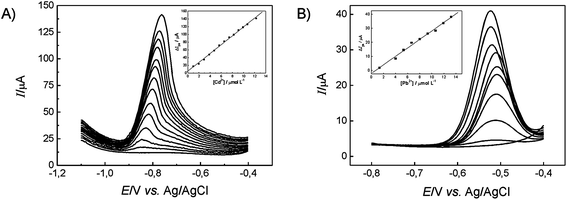 | ||
| Fig. 3 (A) Square-wave anodic stripping voltammograms and analytical curve for Cd determination under the optimum values (frequency 20 Hz, scan potential 10 mV and amplitude 30 mV). Voltammograms for (1) 0.99, (2) 1.96, (3) 2.91, (4) 3.85, (5) 4.76, (6) 5.66, (7) 6.54, (8) 7.41, (9) 8.26, (10) 9.09, (11) 9.91, (12) 10.7 and (13) 12.3 μmol L−1 are shown in sequence. (B) Square-wave anodic stripping voltammograms and analytical curve for Pb(II) determination for selected parameters (frequency 15 Hz, scan potential 3 mV and amplitude 28 mV). Voltammograms for (1) 1.33, (2) 3.99, (3) 5.32, (4) 6.64, (5) 7.97, (6) 9.29 (7) 10.6, (8) 11.9, (9) 13.2 μmol L−1 are shown in sequence. | ||
3.3. Repeatability, reproducibility and interference studies
Repeatability studies were carried out by successive measurements (N = 10) using the sensor in presence of 1.1 × 10⁻⁵ mol L−1 Pb(II) and 5.7 × 10⁻⁵ mol L−1 Cd(II). After each measurement, the working electrode was thoroughly rinsed with water, transferred into the blank electrolyte and scanned in the range of −1.2 to −0.2 V for five cycles to remove any adsorbed species. The continuous use of the electrode, without the surface renewal, yielded a Relative Standard Deviations (RSD) of 1.8% and 2.4% for Pb(II) and Cd(II), respectively. Additionally, the response of the multiple mini-sensors (N = 5) in presence of Pb(II) and Cd(II) ions, at the same above mentioned conditions, was also evaluated. For this case, a RSD smaller than 5% for both appraised metallic ions was obtained, indicating a good performance of the fabricated sensor.Substances with potential interference commonly present in natural waters (NO3−, CO32−, SO42−, Mg2+, Ca2+, Fe3+ and humic acid) were added in the concentration ratios of 10![[thin space (1/6-em)]](https://www.rsc.org/images/entities/char_2009.gif) :1, 1:1 and 1:10 (metallic ions/interferent) in presence of 4.0 × 10⁻⁵ mol L−1 Pb(II) or Cd(II) solutions in order to evaluate the selectivity of the mini-sensor. The voltammetric response for all species evaluated, even in a 10-fold excess, presented less than 5% of interference. Therefore, the commonly inorganic and organic species present in the evaluated samples, do not affect the Cd(II) and Pb(II) determination using the sensor.
:1, 1:1 and 1:10 (metallic ions/interferent) in presence of 4.0 × 10⁻⁵ mol L−1 Pb(II) or Cd(II) solutions in order to evaluate the selectivity of the mini-sensor. The voltammetric response for all species evaluated, even in a 10-fold excess, presented less than 5% of interference. Therefore, the commonly inorganic and organic species present in the evaluated samples, do not affect the Cd(II) and Pb(II) determination using the sensor.
3.4. Application for sensing of lead and cadmium in natural water samples and comparison with the literature
In order to establish the suitability of the proposed method, 1.0 × 10⁻³ mol L−1 of standard Pb(II) or Cd(II) solution was added into the analytical solution with same procedure applied to determine its recovery. The results of which are shown in Table 2 with the recoveries obtained ranging from 95.8 to 105%, suggesting that determining Pb(II) and Cd(II) ions using the proposed mini-sensor has good suitability.| Samples | Pb(II) concentration (μmol L−1) | Cd(II) concentration (μmol L−1) | ||||
|---|---|---|---|---|---|---|
| Added | Found | Recovered (%) | Added | Found | Recovered (%) | |
| A1 | 1.5 ± 0.0 | 1.6 ± 0.1 | 105 | 5.0 ± 0.3 | 5.2 ± 0.9 | 104 |
| A2 | 3.1 ± 0.2 | 3.0 ± 0.1 | 96.8 | 2.4 ± 0.2 | 2.3 ± 0.1 | 95.8 |
| A3 | 6.5 ± 0.2 | 6.6 ± 0.1 | 101 | 3.3 ± 0.2 | 3.4 ± 0.1 | 103 |
| A4 | 11.7 ± 0.2 | 12.1 ± 0.1 | 103 | 1.1 ± 0.2 | 1.1 ± 0.1 | 100 |
In order to evaluate the practical application of the proposed method, the sensor was used as work electrode to determine Cd(II) and Pb(II) ions in natural water samples, collected from river in São Carlos city (Brazil). The water samples were used directly without pre-treatment and the standard addition method was used for Pb(II) and Cd(II) determination. Table 3 shows the results for four samples using the proposed method and the results obtained by FAAS. Applying the t-test for paired data, it was found that all results are in agreement at the 95% confidence level and within acceptable range of errors, confirming the precision and accuracy of the proposed method.
| Samples | Pb(II) concentration (μmol L−1) | Cd(II) concentration (μmol L−1) | ||||
|---|---|---|---|---|---|---|
| Comparative methoda | Proposed method | Relative error % | Comparative methoda | Proposed method | Relative error % | |
| a Determined by FAAS and the RSD (±) was calculated from triplicate. | ||||||
| A1 | 10.0 ± 0.1 | 10.4 ± 0.1 | 4.0 | 5.9 ± 0.1 | 5.8 ± 0.3 | −1.7 |
| A2 | 9.7 ± 0.1 | 9.5 ± 0.0 | −2.1 | 5.8 ± 0.0 | 5.9 ± 0.0 | 1.7 |
| A3 | 11.4 ± 0.1 | 11.4 ± 0.1 | 0.0 | 5.8 ± 0.0 | 5.7 ± 0.2 | −1.7 |
| A4 | 5.4 ± 0.1 | 5.5 ± 0.0 | 1.8 | 3.0± 0.1 |
2.9 ± 0.1 | −3.3 |
The analytical characteristics, such as linear range of the analytical curve (mol L−1) and limit of detection (mol L−1) of the electrode reported in this study and other electrodes from the literature are compared in Table 4 which shows that the min-sensor and analytical protocol is analytically useful.
| Reference | Electrode | Cd LOD mol L−1 | Cd linear range mol L−1 | Pb LOD mol L−1 | Pb linear range mol L−1 |
|---|---|---|---|---|---|
| Slavec et al.40 | Antimony film | 1.7 × 10⁻⁸ | 1.8 × 10⁻⁷ to 8.9 × 10⁻⁷ | 1.5 × 10⁻⁸ | 9.6 × 10⁻⁸ to 4.8 × 10⁻⁷ |
| Sun and Sun41 | Carbon nanotube/nafion | — | — | 5 × 10⁻⁹ | 8 × 10⁻⁸ to 6 × 10⁻⁶ |
| El Mhammedi et al.42 | Platinum/kaolin | 5.4 × 10⁻⁹ | 9.0 × 10⁻⁸ to 8.3 × 10⁻⁶ | — | — |
| Janegitz et al.43 | Carbon nanotube/chitosan | 9.8 × 10⁻⁹ | 5.9 × 10⁻⁸ to 1.5 × 10⁻⁶ | — | — |
| Kadara et al.44 | Bismuth oxide SPE | 4.5 × 10⁻⁸ | 8.9 × 10⁻⁸ to 1.3 × 10⁻⁶ | 4.8 × 10⁻⁸ | 4.8 × 10⁻⁸ to 7.2 × 10⁻⁷ |
| Toghill et al.45 | Antimony nanoparticle/BDD | 3.4 × 10⁻⁷ | 8.9 × 10⁻⁷ to 4.4 × 10⁻⁶ | 1.2 × 10⁻⁷ | 2.4 × 10⁻⁷ to 2.4 × 10⁻⁶ |
| Sherigara et al.46 | Mercury film/carbon paste electrode | — | 5.0 × 10⁻⁹ to 1.0 × 10⁻⁵ | — | 5.0 × 10⁻⁹ to 1.0 × 10⁻⁵ |
| Tarley et al47 | Carbon nanotube | 7.5 × 10⁻⁸ | 5.2 × 10⁻⁷ to 5.7 × 10⁻⁶ | 3.2 × 10⁻⁸ | 2.8 × 10⁻⁷ to 3.1 × 10⁻⁶ |
| This work | BiFE SPE | 5.3 × 10⁻⁷ | 9.9 × 10⁻⁷ to 1.2 × 10⁻⁵ | 8.3 × 10⁻⁷ | 1.3 × 10⁻⁶ to 1.3 × 10⁻⁵ |
4. Conclusions
A copper ex situ plated bismuth film modified electrode has been presented which was found to exhibit a sensitive, precise and accurate response for the sensing of Pb(II) and Cd(II) and was validated with FAAS in natural water samples. The sensor can be economically and mass produced using a portable potentiostat which can be applied for Pb(II) and Cd(II) analysis in situ.Acknowledgements
The authors are gratefull to Fundação de Amparo à Pesquisa do Estado de São Paulo (FAPESP 2008/07529-9 and 2010/20754-1), Conselho Nacional de Desenvolvimento Científico e Tecnológico (CNPq) and Coordenação de Aperfeiçoamento de Pessoal de Nível Superior (CAPES) for financial support.References
- J. P. Metters, R. O. Kadara and C. E. Banks, Analyst, 2011, 136, 1067–1076 RSC.
- I. Palchetti, A. Cagnini, M. Mascini and A. P. F. Turner, Microchim. Acta, 1999, 131, 65–73 CrossRef CAS.
- N. A. Choudhry and C. E. Banks, Anal. Methods, 2011, 3, 74–77 RSC.
- A. Crew, D. Lonsdale, N. Byrd, R. Pittson and J. P. Hart, Biosens. Bioelectron., 2011, 26, 2847–2851 CrossRef CAS.
- E. Y. Z. Frag, G. G. Mohamed, F. A. N. El-Dien and M. E. Mohamed, Analyst, 2011, 136, 332–339 RSC.
- J. Barek, A. G. Fogg, A. Muck and J. Zima, Crit. Rev. Anal. Chem., 2001, 31, 291–309 CrossRef CAS.
- F. Ma, D. Jagner and L. Renman, Anal. Chem., 1997, 69, 1782–1784 CrossRef CAS.
- R. K. Mahajan and N. Kaur, Adsorptive Stripping Voltammetric and Atomic Absorption Spectrometric Evaluation of Nickel in Urine Samples, 1996 Search PubMed.
- P. Kajic, I. Milosev, B. Pihlar and V. Pisot, J. Trace Elem. Med. Biol., 2003, 17, 153–158 CAS.
- A. Economou and P. R. Fielden, Analyst, 2003, 128, 205–212 CAS.
- K. Vytras, I. Svancara and R. Metelka, Electroanalysis, 2002, 14, 1359–1364 CrossRef CAS.
- G. Martinez-Paredes, M. B. Gonzalez-Garcia and A. Costa-Garcia, Electroanalysis, 2009, 21, 925–930 CrossRef CAS.
- L. Lesven, S. M. Skogvold, O. Mikkelsen and G. Billon, Electroanalysis, 2009, 21, 274–279 CrossRef CAS.
- G. H. Hwang, W. K. Han, S. J. Hong, J. S. Park and S. G. Kang, Talanta, 2009, 77, 1432–1436 CrossRef CAS.
- B. C. Janegitz, L. H. Marcolino-Junior and O. Fatibello-Filho, Quim. Nova, 2007, 30, 1673–1676 CrossRef CAS.
- B. C. Janegitz, L. H. Marcolino-Junior, S. P. Campana, R. C. Faria and O. Fatibello-Filho, Sens. Actuators, B, 2009, 142, 260–266 CrossRef.
- O. El Tall, N. Jaffrezic-Renault, M. Sigaud and O. Vittori, Electroanalysis, 2007, 19, 1152–1159 CrossRef CAS.
- A. Charalambous and A. Economou, Anal. Chim. Acta, 2005, 547, 53–58 CrossRef CAS.
- R. Pauliukaite, R. Metelka, I. Svancara, A. Krolicka, A. Bobrowski, K. Vytras, E. Norkus and K. Kalcher, Anal. Bioanal. Chem., 2002, 374, 1155–1158 CrossRef CAS.
- J. Wang and J. M. Lu, Electrochem. Commun., 2000, 2, 390–393 CrossRef CAS.
- S. B. H. E. A. Hutton and B. Ogorevc, Anal. Chim. Acta, 2005, 537, 285–292 CrossRef.
- B. O. E. A. Hutton, F. Weldon, M. R. Smyth and J. Wang, Electrochem. Commun., 2001, 3, 707–711 CrossRef.
- K. N. A. Bobrowski and J. Zarebski, Anal. Chim. Acta, 2005, 543, 150–155 CrossRef.
- A. Economou, TrAC, Trends Anal. Chem., 2005, 24, 334–350 CrossRef CAS.
- K. S. S. Legeai, M. Cretinon, O. Vittori, A. H. D. Oliveira, F. Barbier and M. F. G. Loustalot, Anal. Bioanal. Chem., 2005, 383, 839–847 CrossRef.
- O. V. S. Legeai, Anal. Chim. Acta, 2006, 560, 184–190 CrossRef.
- A. B. A. Krolicka, K. Kalcher, J. Mocak, I. Svancara and K. Vytras, Electroanalysis, 2003, 15, 1859–1863 CrossRef CAS.
- R. P. A. Krolicka, I. Svancara, R. Metelka, A. Bobrowski, E. Norkus, K. Kualcher and K. Vytras, Electrochem. commun., 2002, 4, 193–196 CrossRef.
- E. B. A. S. Arribas, M. Chicharro and A. Zapardiel, Electroanalysis, 2006, 18, 2331–2336 CrossRef.
- L. C. S. de Figueiredo-Filho, V. B. dos Santos, B. C. Janegitz, T. B. Guerreiro, O. Fatibello-Filho, R. C. Faria and L. H. Marcolino-Junior, Electroanalysis, 2010, 22, 1260–1266 CrossRef CAS.
- R. O. Kadara and I. E. Tothill, Anal. Bioanal. Chem., 2004, 378, 770–775 CrossRef CAS.
- J. Wang, Electroanalysis, 2005, 17, 1341–1346 CrossRef CAS.
- Y. Wu, N. B. Li and H. Q. Luo, Sens. Actuators, B, 2008, 133, 677–681 CrossRef.
- S. B. Hocevar, J. Wang, R. P. Deo and B. Ogorevc, Electroanalysis, 2002, 14, 112–115 CrossRef CAS.
- S. Legeai, K. Soropogui, M. Cretinon, O. Vittori, A. H. De Oliveira, F. Barbier and M. F. Grenier-Loustalot, Anal. Bioanal. Chem., 2005, 383, 839–847 CrossRef CAS.
- S. Legeai and O. Vittori, Anal. Chim. Acta, 2006, 560, 184–190 CrossRef CAS.
- L. M. S. Nunes and R. C. Faria, Electroanalysis, 2008, 20, 2259–2263 CrossRef CAS.
- L. C. S. Figueiredo-Filho, D. C. Azzi, B. C. Janegitz and O. Fatibello-Filho, Electroanalysis, 2012, 24, 303–308 CrossRef CAS.
- L. C. S. Figueiredo-Filho, B. C. Janegitz, R. C. Faria, O. Fatibello-Filho, L. H. Marcolino, F. R. Caetano and I. L. de Mattos, Quim. Nova, 2012, 35, 1016–1019 CAS.
- M. Slavec, S. B. Hocevar, L. Baldrianova, E. Tesarova, I. Svancara, B. Ogorevc and K. Vytras, Electroanalysis, 2010, 22, 1617–1622 CrossRef CAS.
- D. Sun and Z. M. Sun, J. Appl. Electrochem., 2008, 38, 1223–1227 CrossRef CAS.
- M. A. El Mhammedi, M. Achak, M. Hbid, M. Bakasse, T. Hbid and A. Chtaini, J. Hazard. Mater., 2009, 170, 590–594 CrossRef CAS.
- B. C. Janegitz, L. C. S. Figueiredo-Filho, L. H. Marcolino-Junior, S. P. N. Souza, E. R. Pereira and O. Fatibello-Filho, J. Electroanal. Chem., 2011, 660, 209–216 CrossRef CAS.
- R. O. Kadara, N. Jenkinson and C. E. Banks, Electroanalysis, 2009, 21, 2410–2414 CAS.
- K. E. Toghill, L. Xiao, G. G. Wildgoose and R. G. Compton, Electroanalysis, 2009, 21, 1113–1118 CrossRef CAS.
- B. S. Sherigara, Y. Shivaraj, R. J. Mascarenhas and A. K. Satpati, Electrochim. Acta, 2007, 52, 3137–3142 CrossRef CAS.
- C. R. T. Tarley, V. S. Santos, B. E. L. Baeta, A. C. Pereira and L. T. Kubota, J. Hazard. Mater., 2009, 169, 256–262 CrossRef CAS.
| This journal is © The Royal Society of Chemistry 2013 |