Low band gap selenophene–diketopyrrolopyrrole polymers exhibiting high and balanced ambipolar performance in bottom-gate transistors†
Munazza
Shahid
a,
Thomas
McCarthy-Ward
a,
John
Labram
b,
Stephan
Rossbauer
b,
Ester Buchaca
Domingo
c,
Scott E.
Watkins
d,
Natalie
Stingelin
c,
Thomas D.
Anthopoulos
b and
Martin
Heeney
*a
aDept. Chemistry and Centre for Plastic Electronics, Imperial College London, London, UK SW7 2AZ. E-mail: m.heeney@imperial.ac.uk
bDept. Physics & Centre for Plastic Electronics, Imperial College London, London, UK SW7 2AZ
cDept. Materials & Centre for Plastic Electronics, Imperial College London, London, UK SW7 2AZ
dCSIRO, Molecular and Health Technologies, VIC 3169, Australia
First published on 1st September 2011
Abstract
We report the synthesis of a selenophene–diketopyrrolopyrrole monomer and its co-polymerisation with selenophene and thieno[3,2-b]thiophene monomers by Stille coupling. The resulting low band gap polymers exhibit ambipolar charge transport in organic field effect transistors. High and balanced electron and hole mobilities in excess of 0.1 cm2 V−1 s−1 were observed in bottom-gate, bottom-contact devices, suggesting that selenophene inclusion is a promising strategy for the development of ambipolar organic semiconductors.
Introduction
Organic semiconductors that are able to transport both holes and electrons efficiently are an attractive approach to the implementation of high-performance CMOS-like circuits.1 CMOS circuits have several advantages over those based upon unipolar logic, including lower power dissipation, greater speed and higher performance.2,3 An ideal ambipolar material should give balanced performance in both the negative and positive voltage regimes and exhibit balanced p- and n-type charge carrier mobility.4 In addition, to simplify circuit design it is desirable to have a common source drain electrode for operation in both the p and n-type regimes to minimize patterning and complex fabrication processes.5 Thus the energetics of the polymer should be tuned such that injection into both the HOMO (for hole injection) and LUMO (for electron injection) is facilitated from a common electrode material. Although high performing ambipolar devices can be prepared from blends of p- and n-type materials,6 such an approach can be complicated by the issue of reproducibly controlling device to device blend morphology and performance, in addition to stabilizing blend morphology to changes over time or operation. Therefore single-component low band gap polymers are of considerable interest for ambipolar applications and several examples have recently been reported with electron and hole mobilities in the range of 2 × 10⁻⁴ to 0.4 cm2 V−1 s−1.7–9One of the most successful strategies to low band gap polymers has been the donor–acceptor approach, whereby strong electron acceptors are co-polymerised with electron-rich donor monomers.10 The resulting polymers show hybridisation of the molecular orbitals, with the LUMO being dominated by the electron accepting unit and the HOMO by the donor material. Following this strategy, low band gap thiophene co-polymers based upon the strong electron acceptor diketopyrrolopyrrole (DPP) have shown recent promise as ambipolar materials.8,9,11–14 However since common electrode materials (for example Au or ITO), have workfunctions (ca. 4.8 eV) more aligned with the polymer HOMO than the LUMO, we were interested to develop approaches to further lower the polymer LUMO to facilitate electron injection, potentially improving electron transport, whilst leaving the HOMO relatively unperturbed.
Design and synthesis
Several groups have recently shown that the replacement of thiophene with selenophene in a polymer backbone results in a reduction in the polymer band gap,15 principally due to the stabilisation of the polymer LUMO, with the HOMO being largely unaffected i.e. the selenophene polymer has more quinoidal character.16 We were interested to explore this approach towards DPP containing co-polymers. We expected that the lower lying LUMO of the selenophene should result in an enhanced mixing of molecular orbitals with the DPP LUMO, and thus an overall lowering of polymer LUMO in comparison to the thiophene analogue. In this article, we report the synthesis of selenophene DPP co-polymers and describe their thin-film properties and ambipolar transistor characteristics.The DPP core is readily synthesised by the condensation reaction of aryl carbonitriles with dialkyl succinate in the presence of base.17 However existing routes to the required 2-cyanoselenophene were complex and involved multiple synthetic steps.18 We therefore adapted a one-pot cyanation procedure originally reported by Lohaus for the cyanation of electron-rich aromatics.19 Thus treatment of a solution of selenophene with chlorosulfonyl isocyanate at 0 °C, followed by work up with DMF afforded selenophene-2-carbonitrile in 76% yield (Scheme 1). Reaction with diisopropyl succinate in the presence of sodium tert-pentoxide afforded the selenophene-substituted DPP as a poorly soluble red solid. In order to ensure good solubility of the resultant polymers, long branched alkyl chains were introduced by alkylation with 1-iodo-2-octyldodecane. Bromination of the resulting monomer with NBS afforded the key intermediate 2,5-di(2-octyldodecyl)-3,6-bis-(5-bromoselenyl)-1,4-diketopyrrolo[3,4-c]pyrrole (1).
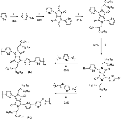 | ||
| Scheme 1 Synthesis of selenophene DPP polymers. Reagents and conditions: (a) (i) ClSO2NCO, (ii) DMF; (b) 0.5 eq. (CH3)2CHCO2(CH2)2CO2CH(CH3)2, 1.7 eq. NaOCH(CH3)2CH2CH3; (c) K2CO3, ICH2CH(C8H17)C10H21; (d) NBS (e) Pd2(dba)3, P(o-tol)3, μW. | ||
The all-selenophene co-polymer, poly(3-(2,2′-biselenophen-5,5′-yl)-2,5-di(2-octyldodecyl)-6-(selenophen-2,5-yl)-1,4-diketopyrrolo[3,4-c]pyrrole (pDPPS3, P1) was synthesised by a Stille polycondensation reaction between 1 and 2,5-bis(trimethylstannyl)selenophene under microwave accelerated conditions (Scheme 1).20Thieno[3,2-b]thiophene was also introduced as a co-monomer in order to enhance backbone co-planarity and promote improved crystallinity to afford poly(3-(2,2′-biselenophen-5,5′-yl)-2,5-di(2-octyldodecyl)-6-(thieno[3,2-b]thiophen-2,5-yl)-1,4-diketopyrrolo[3,4-c]pyrrole (pDPPS2TT, P2). For both P1 and P2 the analogous all-thiophene polymers have been recently reported, pDPPT39 and pDPPT2TT,21 and we make comparison between the properties of the selenophene and thiophene based systems.
Following polymerisation the polymers were purified by precipitation into acidic methanol to cleave any remaining stannyl end groups by protodestannylation, followed by successive Soxhlet extraction with methanol, acetone and hexane, to remove catalyst residues and low molecular weight oligomers. The remaining material was dissolved in chloroform and precipitated into methanol. P1 and P2 were obtained as dark green solids in high yield and high molecular weights (Table 1). Both polymers were soluble in chlorinated solvents like chloroform and chlorobenzene upon heating.
| Polymer | M n/Mwa (kDa) | λ max/nm | ||||
|---|---|---|---|---|---|---|
| CHCl3 | Film | E g b/eV | HOMOc/eV | LUMOd/eV | ||
| a Determined by SEC and reported as their polystyrene equivalents. b Determined by onset of optical absorption. c Determined as a thin film by UV-PESA. d Estimated by the subtraction of the optical band gap from the HOMO. | ||||||
| P1 | 70/210 | 827 | 882 | 1.18 | −5.2 | −4.02 |
| P2 | 100/250 | 823 | 864 | 1.21 | −5.1 | −3.92 |
Thermogravimetric analysis (TGA) was used to evaluate the thermal stability of purified polymers P1 and P2. Both materials demonstrate good thermal stability in air with the onset of decomposition at 385 °C for P1 and 333 °C for P2 (see ESI†).
Results and discussion
Optoelectronic properties
Both polymers exhibited broad optical absorptions in chloroform solution at room temperature, with λmax at 827 and 823 nm for P1 and P2, respectively (Fig. 1). Upon film formation, a bathochromic shift of 55 nm for P1 and 67 nm for P2 was observed, suggestive of backbone planarisation and improved intramolecular order in the solid state. No significant changes were observed upon thermal annealing up to 200 °C, with the absorption remaining broad and featureless (see ESI†). The solid-state optical band gaps, determined by the onset of absorption are 1.18 and 1.20 eV for P1 and P2, respectively. In comparison the respective thiophene analogues of P1 and P2 show solid-state absorption maxima and optical band gaps of 850 nm (1.30 eV) and 825 nm (1.23 eV).9,21 Despite the difficulty in reliably measuring the optical band edge for polymers, it is apparent that the replacement of thiophene with selenophene in the polymer backbone results in a red shift of maximum absorbance and a reduction in polymer band gap, in agreement with earlier theoretical and experimental studies.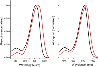 | ||
| Fig. 1 UV-vis absorption spectra of P1 (left) and P2 (right) in solution (chloroform) and in thin films (as-spun from chloroform). | ||
The thin-film ionisation potential of the polymers, as measured by ambient photoelectron spectroscopy (PESA), was 5.2 eV for P1 and 5.1 eV for P2. PESA uses a low power, tuneable UV source to generate photoelectrons that ionise oxygen molecules that are in turn detected by an open counter.22 It has previously been shown that ionisation potentials determined by PESA are comparable with those obtained by other techniques.23 Based upon the optical band gap, we estimate LUMO energy levels of approximately 4 eV for P1 and 3.9 eV for P2. Thus both hole and electron injection from a single common electrode such as Au, should be facilitated.
Electrical properties
The charge transport properties of the polymers were investigated in bottom-gate, bottom-contact (BG, BC) transistor devices, using gold source/drain electrodes and heavily doped silicon as the gate electrode with 200 nm of SiO2 as the gate dielectric. The SiO2 dielectric was treated with hexamethyldisilazane (HMDS) prior to semiconductor deposition, to both passivate the SiO2 surface and enhance the ordering of the semiconductor at the dielectric interface. Films of P1 and P2 were subsequently deposited by spin coating of chlorobenzene solutions. The performances are summarized in Table 2.As-spun films of P1 on HMDS treated substrates showed unipolar (hole only) operation after deposition, with a hole mobility around 10−2 cm2 V−1 s−1. Thermal annealing was found to have a dramatic effect on the charge transport characteristics of the devices converting them from unipolar hole-only to high mobility ambipolar transistors (Fig 2a and b). In particular, the hole mobility was found to saturate after annealing at 100 °C, whereas electron mobility saturated around 200 °C. The evolution of hole and electron mobilities as a function of annealing temperature is displayed in Fig. 2c. Optimized annealed devices demonstrated balanced hole and electron mobilities of 0.1 cm2 V−1 s−1. Although ambipolar polymers with higher mobilities have recently been reported in top gate devices,11 to our knowledge this is the best ambipolar performance reported to date in a BG, BC device, which is generally considered to be a more practical device structure than the top gate one for many micro/opto-electronic applications. The good BG performance is possibly a result of the low lying LUMO levels, which renders the radical anion sufficiently stable that it is not prone to electron trapping at the dielectric interface by reaction with surface silanol groups which are present as a result of incomplete surface passivation.2 The low hydrophilic content of many top-gate insulators is thought to be one reason that many electron transport materials show better performance in top gate devices than bottom gate.
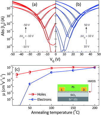 | ||
| Fig. 2 Transfer characteristics of bottom-gate, bottom-contact (BG, BC) organic field-effect transistors (OFETs) with channel length = 10 μm and channel width = 10 mm based on polymer P1. Transfer characteristics measured at VD = −10 V and −50 V (a), and VD = 10 and 50 V (b) at room temperature under N2. (c) Average saturation-regime field-effect mobility of holes and electrons measured in 5 BG, BC OFETs at room temperature after annealing for 30 min at temperatures between 50 and 200 °C. The error bars represent the standard deviation of the measured mobilities. Inset: schematic representation of BG, BC transistor structure used in this study. | ||
Both as-spun and annealed P2 devices also show clear ambipolar characteristics, with as-spun hole and electron mobility of 0.06 and 2 × 10⁻³ cm2 V−1 s−1, respectively. Thermal annealing again resulted in improved performance with peak mobilities around 0.3 and 5 × 10⁻² cm2 V−1 s−1 for holes and electrons after annealing at 250 °C. Similar to P1, hole transport saturated at a lower temperature than electron transport, although the effect was less pronounced (see ESI†).
The origin of the differences in annealing behaviour for holes and electrons in both P1 and P2 may be related to the electronic delocalisation of the HOMO and LUMO, with the LUMO being more localised on the electron-accepting DPP unit than the HOMO. Electron transport relies on efficient interchain overlap of the LUMOs, and is therefore more sensitive to the relative registration of the DPP units between adjacent polymer chains than the HOMO. This relative registration may change on thermal annealing, as has been seen in other electron transporting polymers such as F8BT.24 The differences may also be related to the removal of volatile electron traps from the polymer thin film, with hole transport being less sensitive to the presence of such traps than electron transport.
Further improvements in performance for P2 were observed upon using a top-contact (TC) device configuration, in which Au electrodes were deposited by shadow masking under high vacuum. In combination with an OTS passivation layer, this led to peak mobilities of 1.1 and 0.15 cm2 V−1 s−1 for holes and electrons after annealing at 250 °C. This improvement may be due to reduced contact resistance from the top-contact electrode, in combination with improved polymer ordering at the OTS/polymer dielectric interface. These values are amongst the highest hole mobilities observed for polymeric semiconductors. We were unfortunately unable to form films of P1 on OTS due to dewetting issues. This may be due to the slightly lower molecular weight of P1 relative to P2, or due to the increased alkyl chain density of P1.
We also investigated the air stability of the polymer transistors, since recent results have demonstrated that electron transport can occur under ambient conditions if the polymer LUMO level is below approximately 4 eV.25 However, upon removing BG, BC devices of P2 from the glovebox and measuring in ambient air, a rapid (within 15 min) deterioration in electron transport and mobility was observed, although hole transport was maintained. Electron transport was restored by purging the device under vacuum and measuring in nitrogen.
The transistor performance of the thiophene analogues of P1 and P2 have also been reported. The P1 analogue has a reported hole and electron mobility of 0.04 and 0.01 cm2 V−1 s−1, in BG, BC devices similar to those used here.9,14 The thiophene analogue of P2 has a peak hole mobility of 0.94 cm2 V−1 s−1 after annealing at 200 °C in a bottom-gate, top-contact architecture.21 In this device configuration the electron mobility was described as ‘weak’ and not quantified. Very recently furan analogues of P1 have also been described, with ambipolar transistor behaviour being observed in BG, BC geometry. Mobilities of the order of 10−3 and 10−4 cm2 V−1 s−1 for holes and electrons were observed.13,26 Although exact comparisons are complicated by differences in measurement conditions and device configurations, it is apparent that the inclusion of the larger, more polarisable selenium atom results in significant improvements in electron mobility over both thiophene and furan, whilst the hole mobility is broadly similar. We speculate that these improvements may be related to the delocalisation of the frontier molecular orbitals over the polymer backbone. The HOMO, which is associated with hole transport, is mainly localised over the carbon framework of five-membered heterocycles such as furan, thiophene and selenophene and has no significant density on the heteroatom, whereas the LUMO, which is associated with electron transport, does has signifcant density on the heterocyclic heteroatom.
Thin-film morphology
In order to gain a better understanding of the affects of thermal annealing, the crystallinity of thin films of P1 and P2 was investigated by a combination of WAXS and AFM, both before and after annealing at 200 °C (Fig. 3). For P1 the as-cast film exhibited a diffraction peak at 2θ = 4.5°, which corresponds to a d spacing of 19.6 Å. We assign this to the interchain spacing between polymer main-chains, similar to other conjugated polymers.27 The broad peak around 2θ = 23.5° (d = 3.8 Å) is probably related to π–π stacking of the polymer backbones, and suggests that not all of the polymer backbones are aligned normal to the substrate. Upon annealing at 200 °C, second- and third-order peaks become apparent and the main diffraction peak sharpens and intensifies, consistent with an increase in crystallinity of the film. The layer spacing also increases to 20.5 Å, which may reflect more ordered side-chains with less guache defects. Surprisingly AFM of the films both before and after annealing show little change, with both films exhibiting fine nodule like features on a 20–30 nm scale (Fig. 3).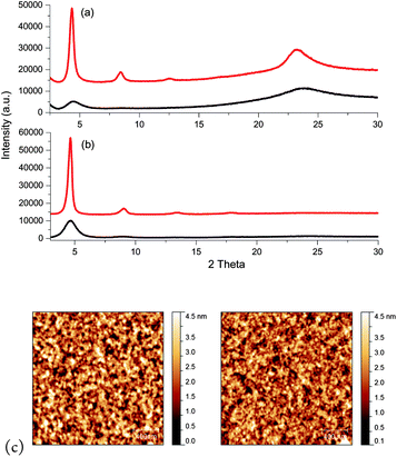 | ||
| Fig. 3 XRD profiles of P1 (a) and P2 (b) thin films spun from chloroform both before (black) and after annealing (red) at 200 °C. (c) Tapping mode AFM height images of P1 (left) and P2 (right) after annealing at 200 °C. | ||
For P2 the diffraction pattern indicates the as-cast polymer has some degree of order, with a main diffraction peak at 2θ = 4.65° corresponding to a d spacing of 19 Å. Unlike P1 there was no peak observable in the π–π region suggesting that the polymer backbone may be well aligned with respect to the substrate, with little misorientation. This is consistent with the high as-spun FET mobilities observed. Upon annealing the peaks sharpen and intensify, with up to four orders of diffraction observable, but the layer spacing does not alter. Similar to P1, the films of P2 exhibit a nodule like morphology by AFM and do not show any significant changes upon annealing.
Conclusions
In conclusion we report the synthesis and characterization of two donor–acceptor selenophene–DPP copolymers and compare their properties to the previously reported thiophene analogues. We find that the incorporation of selenophene results in a reduction in the optical band gap as compared to the thiophene co-polymers, and attribute this to the stabilizing influence of selenophene on the polymer LUMO. XRD results suggest that both polymers form semicrystalline thin films, with increased crystallinity after thermal annealing. Both selenophene co-polymers exhibit excellent ambipolar OFET performance, demonstrating balanced hole and electron mobilities from common Au source–drain electrodes. Importantly high mobilities were observed in readily fabricated bottom-gate, bottom-contact device geometries. These results suggest that the inclusion of the larger and more polarisable Se atom into the polymer backbone has a beneficial effect on electron transport and may be a promising direction for the development of polymers for ambipolar OFETs and integrated circuits.Acknowledgements
This work was carried out in part under the EPSRC grant EP/G060738/1.Notes and references
- J. Zaumseil and H. Sirringhaus, Chem. Rev., 2007, 107, 1296 CrossRef CAS.
- L.-L. Chua, J. Zaumseil, J. F. Chang, E. C.-W. Ou, P. K.-H. Ho, H. Sirringhaus and R. H. Friend, Nature, 2005, 434, 194 CrossRef CAS.
- E. J. Meijer, D. M. De Leeuw, S. Setayesh, E. Van Veenendaal, B. H. Huisman, P. W. M. Blom, J. C. Hummelen, U. Scherf and T. M. Klapwijk, Nat. Mater., 2003, 2, 678 CrossRef CAS.
- Y.-Y. Liu, C.-L. Song, W.-J. Zeng, K.-G. Zhou, Z.-F. Shi, C.-B. Ma, F. Yang, H.-L. Zhang and X. Gong, J. Am. Chem. Soc., 2010, 132, 16349 CrossRef CAS.
- H. Jiang, Macromol. Rapid Commun., 2010, 31, 2007 CrossRef CAS.
- K. Szendrei, D. Jarzab, Z. H. Chen, A. Facchetti and M. A. Loi, J. Mater. Chem., 2010, 20, 1317 RSC; A. Babel, Y. Zhu, K. F. Cheng, W. C. Chen and S. A. Jenekhe, Adv. Funct. Mater, 2007, 17, 2542 CrossRef CAS.
- Y. Zhu, R. D. Champion and S. A. Jenekhe, Macromolecules, 2006, 39, 8712 CrossRef CAS; F. S. Kim, X. G. Guo, M. D. Watson and S. A. Jenekhe, Adv. Mater., 2010, 22, 478 CrossRef; X. G. Guo, R. P. Ortiz, Y. Zheng, Y. Hu, Y. Y. Noh, K. J. Baeg, A. Facchetti and T. J. Marks, J. Am. Chem. Soc., 2011, 133, 1405 CrossRef; Z. Y. Chen, H. Lemke, S. Albert-Seifried, M. Caironi, M. M. Nielsen, M. Heeney, W. M. Zhang, I. McCulloch and H. Sirringhaus, Adv. Mater., 2010, 22, 2371 CrossRef; H. Usta, C. Risko, Z. M. Wang, H. Huang, M. K. Deliomeroglu, A. Zhukhovitskiy, A. Facchetti and T. J. Marks, J. Am. Chem. Soc., 2009, 131, 5586 CrossRef; X. Zhang, T. T. Steckler, R. R. Dasari, S. Ohira, W. J. Potscavage, S. P. Tiwari, S. Coppee, S. Ellinger, S. Barlow, J. L. Bredas, B. Kippelen, J. R. Reynolds and S. R. Marder, J. Mater. Chem., 2010, 20, 123 RSC; T. T. Steckler, X. Zhang, J. Hwang, R. Honeyager, S. Ohira, X. H. Zhang, A. Grant, S. Ellinger, S. A. Odom, D. Sweat, D. B. Tanner, A. G. Rinzler, S. Barlow, J. L. Bredas, B. Kippelen, S. R. Marder and J. R. Reynolds, J. Am. Chem. Soc., 2009, 131, 2824 CrossRef; Z. Y. Chen, J. F. Fang, F. Gao, T. J. K. Brenner, K. K. Banger, X. Z. Wang, W. T. S. Huck and H. Sirringhaus, Org. Electron., 2011, 12, 461 CrossRef; R. Mondal, N. Miyaki, H. A. Becerril, J. E. Norton, J. Parmer, A. C. Mayer, M. L. Tang, J. L. Bredas, M. D. McGehee and Z. A. Bao, Chem. Mater., 2009, 21, 3618 CrossRef.
- L. Burgi, M. Turbiez, R. Pfeiffer, F. Bienewald, H. J. Kirner and C. Winnewisser, Adv. Mater., 2008, 20, 2217 CrossRef CAS.
- J. C. Bijleveld, A. P. Zoombelt, S. G. J. Mathijssen, M. M. Wienk, M. Turbiez, D. M. de Leeuw and R. A. J. Janssen, J. Am. Chem. Soc., 2009, 131, 16616 CrossRef CAS.
- Y. J. Cheng, S. H. Yang and C. S. Hsu, Chem. Rev., 2009, 109, 5868 CrossRef CAS.
- P. Sonar, S. P. Singh, Y. Li, M. S. Soh and A. Dodabalapur, Adv. Mater., 2010, 22, 5409 CrossRef CAS; R. S. Ashraf, Z. Y. Chen, D. S. Leem, H. Bronstein, W. M. Zhang, B. Schroeder, Y. Geerts, J. Smith, S. Watkins, T. D. Anthopoulos, H. Sirringhaus, J. C. de Mello, M. Heeney and I. McCulloch, Chem. Mater., 2011, 23, 768 CrossRef.
- A. P. Zoombelt, S. G. J. Mathijssen, M. G. R. Turbiez, M. M. Wienk and R. A. J. Janssen, J. Mater. Chem., 2010, 20, 2240 RSC; H. Bronstein, Z. Y. Chen, R. S. Ashraf, W. M. Zhang, J. P. Du, J. R. Durrant, P. S. Tuladhar, K. Song, S. E. Watkins, Y. Geerts, M. M. Wienk, R. A. J. Janssen, T. Anthopoulos, H. Sirringhaus, M. Heeney and I. McCulloch, J. Am. Chem. Soc., 2011, 133, 3272 CrossRef CAS.
- J. C. Biljlevled, B. P. Karsten, S. G. J. Mathijssen, M. M. Wienk, D. M. de Leeuw and R. A. J. Janssen, J. Mater. Chem., 2011, 21, 1600 RSC.
- W. S. C. Roelofs, S. G. J. Mathijssen, J. C. Bijleveld, D. Raiteri, T. C. T. Geuns, M. Kemerink, E. Cantatore, R. A. J. Janssen and D. M. de Leeuw, Appl. Phys. Lett., 2011, 98, 203301 CrossRef.
- D. J. Crouch, P. J. Skabara, J. E. Lohr, J. J. W. McDouall, M. Heeney, I. McCulloch, D. Sparrowe, M. Shkunov, S. J. Coles, P. N. Horton and M. B. Hursthouse, Chem. Mater., 2005, 17, 6567 CrossRef CAS; M. Heeney, W. Zhang, D. J. Crouch, M. L. Chabinyc, S. Gordeyev, R. Hamilton, S. J. Higgins, I. McCulloch, P. J. Skabara, D. Sparrowe and S. Tierney, Chem. Commun., 2007, 5061 RSC; A. Patra and M. Bendikov, J. Mater. Chem., 2010, 20, 422 RSC; Y. H. Wijsboom, A. Patra, S. S. Zade, Y. Sheynin, M. Li, L. L. W. Shimon and M. Bendikov, Angew. Chem., Int. Ed., 2009, 48, 5443 CrossRef; A. Patra, Y. H. Wijsboom, S. S. Zade, M. Li, Y. Sheynin, G. Leitus and M. Bendikov, J. Am. Chem. Soc., 2008, 130, 6734 CrossRef.
- S. S. Zade, N. Zamoshchik and M. Bendikov, Chem.–Eur. J., 2009, 15, 8613 CrossRef CAS.
- Z. Hao and A. Iqbal, Chem. Soc. Rev., 1997, 26, 203 RSC.
- Y. K. Yur'ev and N. N. Mezentsova, Zh. Obshch. Khim., 1958, 28 Search PubMed.
- G. Lohaus, Chem. Ber., 1967, 100, 2719 CrossRef CAS.
- S. Tierney, M. Heeney and I. McCulloch, Synth. Met., 2005, 148, 195 CrossRef CAS.
- Y. N. Li, S. P. Singh and P. Sonar, Adv. Mater., 2010, 22, 4862 CrossRef CAS.
- H. Kirihata and M. Uda, Rev. Sci. Instrum., 1980, 52, 68 CrossRef.
- R. J. Davis, M. T. Lloyd, S. R. Ferreira, M. J. Bruzek, S. E. Watkins, M. Fahlman, J. E. Anthony and J. W. P. Hsu, J. Mater. Chem, 2011, 21, 1721 RSC.
- C. L. Donley, J. Zaumseil, J. W. Andreasen, M. M. Nielsen, H. Sirringhaus, R. H. Friend and J.-S. Kim, J. Am. Chem. Soc., 2005, 127, 12890 CrossRef CAS.
- H. Usta, A. Facchetti and T. J. Marks, J. Am. Chem. Soc., 2008, 130, 8580 CrossRef CAS.
- C. H. Woo, P. M. Beaujuge, T. W. Holcombe, O. P. Lee and J. M. J. Frechet, J. Am. Chem. Soc., 2010, 132, 15547 CrossRef CAS.
- A. Salleo, R. J. Kline, D. M. DeLongchamp and M. L. Chanbinyc, Adv. Mater., 2010, 22, 3812 CrossRef CAS.
Footnote |
| † Electronic supplementary information (ESI) available. See DOI: 10.1039/c1sc00477h |
| This journal is © The Royal Society of Chemistry 2012 |