TiO2-decorated graphenes as efficient photoswitches with high oxygen sensitivity†
Qing
Wang
a,
Xuefeng
Guo
*bc,
Lichao
Cai
b,
Yang
Cao
b,
Lin
Gan
b,
Song
Liu
b,
Zhenxing
Wang
b,
Hongtao
Zhang
b and
Lidong
Li
*a
aSchool of Materials Science and Engineering, University of Science and Technology Beijing, Beijing, 100083, P. R. China. E-mail: lidong@mater.ustb.edu.cn
bCenter for Nanochemistry, Beijing National Laboratory for Molecular Sciences, State Key Laboratory for Structural Chemistry of Unstable and Stable Species, College of Chemistry and Molecular Engineering, Peking University, Beijing, 100871, P. R. China. E-mail: guoxf@pku.edu.cn; Tel: (+86) 10-62757789
cDepartment of Advanced Materials and Nanotechnology, College of Engineering, Peking University, Beijing, 100871, P. R. China
First published on 21st July 2011
Abstract
We detail a facile fabrication and testing method of functionalizing single-layer graphenes (SLGs) by photoactive TiO2 thin films as test-beds for building efficient multifunctional optoelectronic devices. Interestingly, tuning the photoactivity of TiO2 enables us to realize fast and significant photoswitching effects in TiO2-graphene devices. More importantly, using the hybrid devices as solid-state gas sensors, we have demonstrated a reversible and linear electrical sensitivity towards oxygen gas in the full concentration range (5–100%) at room temperature and ambient pressure, with a calculated minimum detection limit (MDL) of 0.01% oxygen. The unique oxygen sensitivity of the devices is attributed to the synergetic effect of the photoactivity of TiO2 and the environmental ultrasensitivity of SLGs. These results form the basis for new types of future ultrasensitive multifunctional integrated devices for a variety of possible detection and/or sensing applications.
Introduction
Integrating nanoscale materials, such as nanotubes and nanowires, into functional optoelectronic devices capable of converting external stimuli to easily detectable electrical signals is becoming one of the hottest areas in the fields of micro/nanoelectronics due to their potential applications in switching, detecting and sensing systems.1 In particular, considerable interest has been very recently attracted to the incorporation of the emergent nanomaterial graphene as sensing elements.2,3 This is because single-layer graphene (SLG) has the simplest chemical composition and atomic bonding configuration in a two-dimensional (2D) manner that maximizes its surface-to-volume ratio. Each carbon atom on the surface of SLG is exposed to the environment and any tiny changes from the environment could cause drastic changes in its electrical properties. In conjunction with its high conductivity, high chemical stability, and ease of micro/nanofabrication, the environmental ultrasensitivity places graphene as a promising platform for creating new types of sensors and optoelectronic devices.4Molecular oxygen is a ubiquitous requirement for human life so monitoring the ambient oxygen level is of crucial importance for a wide variety of civilian and military applications. Numerous technologies have been developed for oxygen detection, including electrochemistry, optical spectroscopy and solid-state chemically sensitive semiconductors.5 Among the detection approaches developed so far, some require high operating temperatures or high vacuum conditions; some suffer from the complicated fabrication techniques; and others lack high sensitivity. As a result, researchers have worked to develop robust low-cost device platforms to detect oxygen at room temperature and ambient pressure. To this end, we describe in this study a simple method to fabricate efficient stimuli-responsive optoelectronic devices with unique high oxygen sensitivity. These functional devices are formed from SLGs that are decorated with photoactive TiO2 thin films (Fig. 1a). The well-known feature of unique TiO2 thin films that we utilize here is that UV irradiation generates free electrons (e−) and holes (h+) as the active centers on the nanocrystal surface.6 We and others have previously investigated whether these carriers are able to improve and/or fine-tune the electrical properties of organic or nanotube-based transistors.7 Interestingly, the TiO2-decorated SLG transistors show fast and large conductance decrease upon exposure to UV light, the decrease reverses when the UV irradiation is switched off. Importantly, after a preliminary illumination of UV light to populate carrier traps at the interface between graphene and TiO2 thin film, the activated devices show a reversible and linear electrical sensitivity towards oxygen gas in a full concentration range (5–100%) when they operate at room temperature and ambient pressure, which represents a significant step in the development of practical low-cost detection platforms for oxygen.
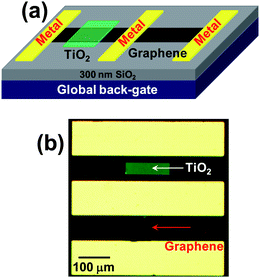 | ||
| Fig. 1 (a) Schematic representation of a SLG transistor decorated by TiO2 thin films and a pristine SLG transistor as control. (b) An optical image of a representative SLG device coated by a 5-nm TiO2 thin film and a control SLG device. | ||
Results and discussion
CVD-grown SLG-based transistors were fabricated using a nondestructive method through a polymer-mediated transfer technique and selective oxygen plasma etching developed elsewhere.8 This method allows to mass-produce SLG transistor arrays with high quality and high yield (Fig. S1, ESI†). The statistical device resistance is in the range of 0.2–1.0 kΩ (Fig. S2, ESI†). After the initial electrical characterization, we deposited a 5 nm-thick TiO2 thin film (150 μm long and 60 μm wide) on graphene surfaces by electron beam (e-beam) lithography followed by e-beam thermal evaporation. High-resolution transmission electron microscopic (TEM) investigations reveal that these thin films consist of numerous TiO2 nanoparticles with the diameter of less than 5 nm in either anatase or rutile crystalline form (approximately 2![[thin space (1/6-em)]](https://www.rsc.org/images/entities/char_2009.gif) :1) (Fig. 2 and S3, ESI†).9 In the two crystalline forms of TiO2, rutile is the most stable phase, whereas anatase has the superior optoelectronic and photochemical properties,6 implying the useful optoelectronic properties described below. To rule out potential artifacts from Schottky barrier modification, we narrowed TiO2 thin films to disconnect them with metal electrodes as demonstrated in Fig. 1b. To aid in the subsequent analysis of the devices, we kept the neighboring device pristine as control (Fig. 1b). In this case, we are able to simultaneously characterize and compare the stimuli-responsive properties of both functional and control devices at the same operation conditions, thus ensuring the measurement reliability. To carry out the measurements efficiently, we designed and made a novel sealed blackbox, which has a quartz window used for light stimulation, two channels for gas flow, and multiple connectors for electrical characterization (Fig. 3). By using this home-made testing platform, we are able to simultaneously generate two or more external stimuli, such as light and gas, to the devices under test. Through a simple wire-bonding method, the newly-made devices were then incorporated into the testing system. Before sensing measurements, we purged the system by a stream of N2 gas to completely remove any trace of air or oxygen in the chamber.
:1) (Fig. 2 and S3, ESI†).9 In the two crystalline forms of TiO2, rutile is the most stable phase, whereas anatase has the superior optoelectronic and photochemical properties,6 implying the useful optoelectronic properties described below. To rule out potential artifacts from Schottky barrier modification, we narrowed TiO2 thin films to disconnect them with metal electrodes as demonstrated in Fig. 1b. To aid in the subsequent analysis of the devices, we kept the neighboring device pristine as control (Fig. 1b). In this case, we are able to simultaneously characterize and compare the stimuli-responsive properties of both functional and control devices at the same operation conditions, thus ensuring the measurement reliability. To carry out the measurements efficiently, we designed and made a novel sealed blackbox, which has a quartz window used for light stimulation, two channels for gas flow, and multiple connectors for electrical characterization (Fig. 3). By using this home-made testing platform, we are able to simultaneously generate two or more external stimuli, such as light and gas, to the devices under test. Through a simple wire-bonding method, the newly-made devices were then incorporated into the testing system. Before sensing measurements, we purged the system by a stream of N2 gas to completely remove any trace of air or oxygen in the chamber.
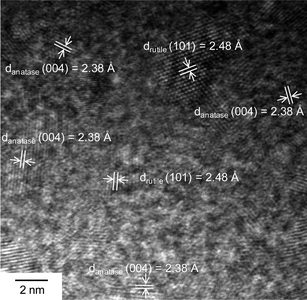 | ||
| Fig. 2 A high-resolution TEM image of a 5 nm-thick TiO2 thin film formed through e-beam thermal evaporation. | ||
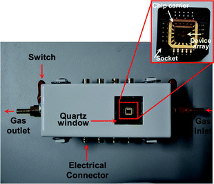 | ||
| Fig. 3 Schematic illustration of our home-made blackbox designed for the purpose of sensing measurements. Inset shows how the devices under test are connected to the testing system through a wire-bonding method. | ||
Fig. 4a shows the source–drain current (ID) as a function of the gate voltage (VG) at a fixed source–drain bias voltage (VD) for a representative device in each step of the operations. To eliminate possible artifacts from gate hysteresis, all of the current–voltage curves (I–V) were acquired on the same measurement cycle while scanning from positive to negative bias. We observed very stable I–V curves for these devices in fixed experimental conditions, thus they can be used to detect photoswitching and sensing functions. We note that, due to chemical doping and/or charge transfer induced by etching agents and polymer resists (iron nitrate and polymethyl methracrylate),8 the resulting graphenes only behave as p-type semiconductors (Fig. 4a). After TiO2 thin film deposition, the devices showed slight conductance decrease (red curve in Fig. 4a), most likely due to the scattering effect for carriers created by TiO2 thin films that are intimately covered on graphene surfaces. Once SLG transistors were decorated by TiO2 thin films, the device characteristics became very sensitive to UV light. We observed the reversible, fast, and significant changes in ID when the devices were measured under UV irradiation and in the dark. Fig. 4 shows such a photoswitching effect in a device when a handheld UV lamp (254 nm, a low intensity of ca. 50 μW cm−2) was switched on and off. Noticeably, upon UV irradiation, dramatic decrease in ID occurred regardless of the gate bias (blue curve in Fig. 4a). The incident UV light generated free electron–hole pairs at the graphene/TiO2 thin film interface.6 It is unlikely that the significant changes in ID result from Schottky barrier height modification caused by photoinduced electron–hole pairs or oxygen desorption at metal-graphene junctions1b,10 because all the measurements mentioned above were performed under the protection of inert N2 gas using the device structure where TiO2 thin films are not connected with metal electrodes. Simultaneous control experiments using pristine graphene transistors did not show obvious current changes when UV light was switched on and off at the same condition (black curve in Fig. 4b), thus precluding the possibility of intrinsic photoresponses of graphenes, that could be detected by using high-intensity laser lights for building ultrafast photodetectors.11 Note that we failed to perform control experiments using only 5 nm-thick TiO2 thin films because they are insulating due to the uncontinuity. On the basis of earlier work on photoinduced charge transfer at the semiconductor/dielectric interface by Calhoun and ours,7 therefore, we conclude that the photogenerated electrons at the interface behave like a Coulomb trap and quench p-type carriers, thus lowering the carrier mobility in graphene transistors.
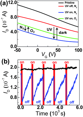 | ||
| Fig. 4 (a) Device characteristics of a representative device in each step of sequential operations. Black: pristine graphene; Red: TiO2-decorated graphene; Blue: after UV exposure; Green: after further oxygen exposure (high-purity, 99.99%). VD = 400 μV. (b) Simultaneously recorded ID for a TiO2-decorated graphene (blue) and pristine graphene (black) while UV light was toggled on and off; VD = 100 μV, VG = 0 V. | ||
Remarkably, when kept in the dark after UV irradiation, its drain current of the same device was essentially restored to its original value. We found that the back-and-forth photoswitching effect is rather gradual in time. The blue curve in Fig. 4b shows five representative switching cycles of the same device when UV light is toggled on and off. The drain current sharply decreased at the beginning of UV irradiation and was saturated after ∼100 s of exposure when TiO2 thin films reached the maximum of photogenerated charge separation. On the contrary, after the low-conductance state was established and the device was kept in the dark, the device presented a slow current relaxation, completing the increase after ∼15 min. This can be explained by the progressive detrapping of holes on the surface of TiO2 thin films by electrons that originate from the conductive channel where the p-type transistors have a very low density of electrons. These photoswitching phenomena are quite reproducible as the yield of working devices is very high (almost 30 out of ∼31 devices). The reliability and mechanistic understanding of the photoswitching phenomena discussed above set the foundation for following cyclable gas detection.
Oxygen has been proven to behave as electron traps after adsorption on many semiconductor surfaces, such as In2O3 nanocrystals and Ga2O3 nanowires,5d,12 by forming the negatively charged ion state. In the current case, TiO2 photoexcitation produces excited-state electron–hole pairs, which can then react with analytes adsorbed onto the surface. Consequently, we suggest that further exposure of UV-activated devices to oxygen results in the reaction [O2(g) + e− → O2−(ad)] and the formation of oxygen anions on the surface. The formation of oxygen anions removes TiO2 hole traps, increases the density of hole carriers in graphene and thus leads to the partial restoration of the device conductance (green curve in Fig. 4a). From the data before and after oxygen exposure (high-purity, 99.99%) in Fig. 4a, we calculated the ratio of the current change (ΔI) to the initial value (IO). On the basis of the gate-dependent spectrum of ΔI/IO in Fig. S4 (ESI†), we estimated the optimized operational gate voltage to be in the range of 50–80 V. To avoid the possible damage and/or heating effect at high voltages, we then fixed gate bias at 50 V for the following measurements. We found that the sensing behavior is fully reversible under the optimized condition. Fig. 5a shows five representative sensing cycles for a TiO2-decorated graphene when sequentially exposed to high-purity oxygen (99.99%) and nitrogen under continuous UV irradiation. The response time, τres, and recovery time, τrec, defined as the time necessary to reach 95% of the final current value,5d are ∼130 and 260 s, respectively, which is quite fast considering the low operating temperature.1a,5d–f The fast sensibility and good reversibility only with a slight increase of the recovery time over cycles indicate that TiO2-decorated graphenes experienced only negligible photodegradation or chemical damage during operations. Simultaneous control experiment using pristine graphene devices did not show any response to oxygen at the same operation conditions (black curve in Fig. 5a). Further control experiments using either TiO2-decorated or pristine graphenes but without UV irradiation also showed the negligible changes in ID of devices upon exposure to oxygen (Fig. S5, ESI†). These results prove that UV illumination is a prerequisite for oxygen sensing application.
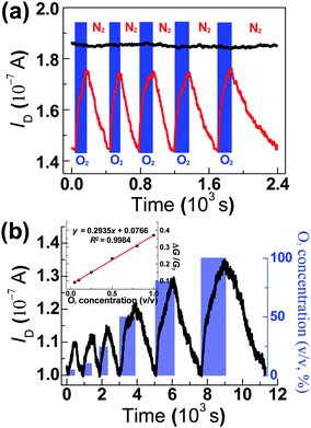 | ||
| Fig. 5 (a) Representative sensing cycles of a TiO2-decorated graphene (red) and pristine graphene (black) devices upon sequential exposure to high-purity oxygen (99.99%) and nitrogen under continuous UV irradiation; VD = 200 μV, VG = 50 V. (b) A concentration-dependent spectrum of a TiO2-decorated graphene device under UV irradiation. Inset shows the linear response of the device to oxygen during exposure cycles; VD = 100 μV, VG = 50 V. | ||
To summarize the proposed response mechanism (Fig. 6), we suggest that the photoexcitation of TiO2 thin films activates TiO2 ground-state electrons into an excited state, which subsequently produce scattering sites for hole carriers that flow through graphenes. These active scattering sites can quench hole carriers and therefore lower the mobility in p-type semiconductor devices. However, the introduction of oxygen gas leads to the formation of negatively charged oxygen anions by the reaction between the activated electron and oxygen. This decreases the scattering sites, releases hole carriers back into the conducting channel and therefore reverses the high conductance state of graphenes.
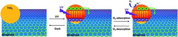 | ||
| Fig. 6 Mechanistic illustration of the hybrid devices when exposed to UV light and oxygen gas. | ||
Using these stable TiO2-decorated graphenes, we are able to explore their oxygen sensitivity. We found a linear electrical response to oxygen gas in the nearly full concentration range (5–100%) (Fig. 5b). To establish the consistent baseline before measurement, we performed preliminary UV illumination for 8 min to stabilize the devices at the arbitrary low conductance state (GO). Then, sequential introduction of oxygen gas (diluted in nitrogen) while keeping UV irradiation during measurement produced a concentration-dependent increase in the TiO2-decorated graphene devices (Fig. 5b). Each oxygen exposure was extended to fully reach its maximum equilibrium and followed by nitrogen purging to recover its arbitrarily defined low conductance state. On the basis of the standard deviation in the low conductance state before the oxygen exposure, we estimated a signal-to-noise ratio of 3.65 for the device response to 5% oxygen. From the changes in current after oxygen exposure, the ratio of conductance changes (ΔG/GO) as a function of oxygen concentration can be calculated as shown in Fig. 5b, inset. We found that the ratio of conductance changes scaled up with the concentration of oxygen. Again, the linear response and repeated recovery to the low conductance state indicate the long-term operation ability of our devices without any degradation. Using a value three times the standard deviation of the low conductance state as the minimum detection limit (MDL), we achieved the MDL of approximately 0.01% oxygen for our unoptimized devices, suggesting that this system hold promise as a robust low-temperature platform for monitoring trace amounts of oxygen under the specific conditions.1b,2a,12
Conclusion
In summary, we have established a reliable fabrication and testing method of functionalizing SLGs by a photoactive TiO2 thin film as test-beds for building efficient multifunctional optoelectronic devices. It is remarkable that tuning the photoactivity of TiO2 realizes fast and significant photoswitching effects in TiO2-graphene devices. Using the hybrid devices as solid-state gas sensors, we have demonstrated a reversible and linear electrical sensitivity towards oxygen gas in the full concentration range (5–100%) at room temperature and ambient pressure, with a calculated MDL of 0.01% oxygen. The unique oxygen sensitivity of the devices is attributed to the synergetic effect of the photoactivity of TiO2 and the inherent ultrasensitivity of SLGs. The ease of device fabrication, the reproducibility, and the achievement of fast photoswitching and high oxygen sensitivity results imply that graphene-based hybrid materials could serve as a promising platform for developing low-cost, portable and sensitive device arrays for detecting light, oxygen and many other molecules.4 In addition, the sensing mechanistic understanding and the concept of incorporating molecular functionalities into optoelectronic circuits in this study should provide new insights into designing new types of future ultrasensitive multifunctional integrated devices for potential applications in both industrial and scientific communities, for example, environmental monitoring, national defense, remote control, optical telecommunication, day- and night-time surveillance, and health protection.Experimental
We synthesized high-quality SLGs through a chemical vapor deposition (CVD) process on copper foils. Through a polymer-mediated transfer technique and selective oxygen plasma etching, we are able to mass-produce SLG transistor arrays with high yield. Experimental details can be found in the literature.8 After the initial electrical characterization, 5 nm-thick TiO2 thin films (150 μm long and 60 μm wide) were deposited on graphene surfaces patterned by electron beam (e-beam) lithography followed by e-beam thermal evaporation. To rule out potential artifacts from Schottky barrier modification, we narrowed TiO2 thin films to disconnect them with metal electrodes. To aid in the subsequent analysis of the devices, we kept the neighboring device pristine as control. To carry out the measurements efficiently, we designed and made a novel sealed blackbox (Fig. 3), which has a quartz window used for light stimulation, two channels for gas flow, and multiple connectors for electrical characterization. Through a simple wire-bonding method, the fresh devices were then incorporated into the testing system. The device characterization was carried out at room temperature and atmospheric pressure using an Agilent 4155C semiconductor characterization system and a Karl Suss (PM5) manual probe station. For photoswitching experiments, light irradiations were performed with a handheld UV lamp (∼50 μW cm−2, λ = 254 nm). For sensing measurements, high-purity oxygen (99.99%) was used. Before sensing measurements, we purged the system by a stream of pure N2 gas to completely remove any trace of air or oxygen in the chamber.Acknowledgements
We acknowledge primary financial support from MOST (2009CB623703), MOE (NCET-08-0725, FRF-TP-09-011B), NSFC (Grant No. 50821061, 20833001, 2112016, and 90923015), 111 Project (B08001) and BSTSP (2009A01).Notes and references
- (a) J. Kong, N. R. Franklin, C. W. Zhou, M. G. Chapline, S. Peng, K. J. Cho and H. J. Dai, Science, 2000, 287, 622–625 CrossRef CAS; (b) P. G. Collins, K. Bradley, M. Ishigami and A. Zettl, Science, 2000, 287, 1801–1804 CrossRef CAS; (c) Y. L. Zhao and J. F. Stoddart, Acc. Chem. Res., 2009, 42, 1161–1171 CrossRef CAS; (d) A. K. Feldman, M. L. Steigerwald, X. Guo and C. Nuckolls, Acc. Chem. Res., 2008, 41, 1731–1741 CrossRef CAS; (e) F. Patolsky, B. P. Timko, G. Yu, Y. Fang, A. B. Greytak, G. Zheng and C. M. Lieber, Science, 2006, 313, 1100–1104 CrossRef CAS; (f) K. J. Choi and H. W. Jang, Sensors, 2010, 10, 4083–4099 CrossRef CAS; (g) D. R. Kauffman and A. Star, Angew. Chem., Int. Ed., 2008, 47, 6550–6570 CrossRef CAS; (h) S. Liu, Q. Shen, Y. Cao, L. Gan, Z. X. Wang, M. L. Steigerwald and X. F. Guo, Coord. Chem. Rev., 2010, 254, 1101–1116 CrossRef CAS.
- (a) F. Schedin, A. K. Geim, S. V. Morozov, E. W. Hill, P. Blake, M. I. Katsnelson and K. S. Novoselov, Nat. Mater., 2007, 6, 652–655 CrossRef CAS; (b) Y. P. Dan, Y. Lu, N. J. Kybert, Z. T. Luo and A. T. C. Johnson, Nano Lett., 2009, 9, 1472–1475 CrossRef CAS; (c) J. D. Fowler, M. J. Allen, V. C. Tung, Y. Yang, R. B. Kaner and B. H. Weiller, ACS Nano, 2009, 3, 301–306 CrossRef CAS; (d) Q. Y. He, H. G. Sudibya, Z. Y. Yin, S. X. Wu, H. Li, F. Boey, W. Huang, P. Chen and H. Zhang, ACS Nano, 2010, 4, 3201–3208 CrossRef CAS; (e) Y. Ohno, K. Maehashi, Y. Yamashiro and K. Matsumoto, Nano Lett., 2009, 9, 3318–3322 CrossRef CAS; (f) V. Dua, S. P. Surwade, S. Ammu, S. R. Agnihotra, S. Jain, K. E. Roberts, S. Park, R. S. Ruoff and S. K. Manohar, Angew. Chem., Int. Ed., 2010, 49, 2154–2157 CrossRef CAS; (g) X. C. Dong, Y. M. Shi, W. Huang, P. Chen and L. J. Li, Adv. Mater., 2010, 22, 1649–1653 CrossRef CAS; (h) N. Mohanty and V. Berry, Nano Lett., 2008, 8, 4469–4476 CrossRef CAS; (i) T. Cohen-Karni, Q. Qing, Q. Li, Y. Fang and C. M. Lieber, Nano Lett., 2010, 10, 1098–1102 CrossRef CAS; (j) D. Wei, Y. Liu, H. Zhang, L. Huang, B. Wu, J. Chen and G. Yu, J. Am. Chem. Soc., 2009, 131, 11147–11154 CrossRef CAS; (k) Y. Shao, J. Wang, H. Wu, J. Liu, I. A. Aksay and Y. Lin, Electroanalysis, 2010, 22, 1027–1036 CAS; (l) J. Dai and J. Yuan, Phys. Rev. B: Condens. Matter Mater. Phys., 2010, 81, 165414 CrossRef; (m) R. K. Joshi, H. Gomez, F. Alvi and A. Kumar, J. Phys. Chem. C, 2010, 114, 6610–6613 CrossRef CAS.
- (a) P. K. Ang, W. Chen, A. T. S. Wee and K. P. Loh, J. Am. Chem. Soc., 2008, 130, 14392–14393 CrossRef CAS; (b) C. H. Lu, H. H. Yang, C. L. Zhu, X. Chen and G. N. Chen, Angew. Chem., Int. Ed., 2009, 48, 4785–4787 CrossRef CAS; (c) X. C. Dong, D. L. Fu, W. J. Fang, Y. M. Shi, P. Chen and L. J. Li, Small, 2009, 5, 1422–1426 CrossRef CAS; (d) G. H. Lu, L. E. Ocola and J. H. Chen, Appl. Phys. Lett., 2009, 94, 083111 CrossRef; (e) J. T. Robinson, F. K. Perkins, E. S. Snow, Z. Q. Wei and P. E. Sheehan, Nano Lett., 2008, 8, 3137–3140 CrossRef CAS; (f) M. Qazi, T. Vogt and G. Koley, Appl. Phys. Lett., 2007, 91, 233101 CrossRef; (g) R. Arsat, M. Breedon, M. Shafiei, P. G. Spizziri, S. Gilje, R. B. Kaner, K. Kalantar-Zadeh and W. Wlodarski, Chem. Phys. Lett., 2009, 467, 344–347 CrossRef CAS; (h) A. N. Cao, Z. Liu, S. S. Chu, M. H. Wu, Z. M. Ye, Z. W. Cai, Y. L. Chang, S. F. Wang, Q. H. Gong and Y. F. Liu, Adv. Mater., 2010, 22, 103–106 CrossRef CAS; (i) X. M. Geng, L. Niu, Z. Y. Xing, R. S. Song, G. T. Liu, M. T. Sun, G. S. Cheng, H. J. Zhong, Z. H. Liu, Z. J. Zhang, L. F. Sun, H. X. Xu, L. Lu and L. W. Liu, Adv. Mater., 2010, 22, 638–642 CrossRef CAS; (j) Y. Lin, K. Zhang, W. F. Chen, Y. D. Liu, Z. G. Geng, J. Zeng, N. Pan, L. F. Yan, X. P. Wang and J. G. Hou, ACS Nano, 2010, 4, 3033–3038 CrossRef CAS.
- (a) A. K. Geim, Science, 2009, 324, 1530–1534 CrossRef CAS; (b) W. R. Yang, K. R. Ratinac, S. P. Ringer, P. Thordarson, J. J. Gooding and F. Braet, Angew. Chem., Int. Ed., 2010, 49, 2114–2138 CrossRef CAS; (c) C. N. R. Rao, A. K. Sood, K. S. Subrahmanyam and A. Govindaraj, Angew. Chem., Int. Ed., 2009, 48, 7752–7777 CrossRef CAS; (d) K. P. Loh, Q. L. Bao, P. K. Ang and J. X. Yang, J. Mater. Chem., 2010, 20, 2277–2289 RSC; (e) D. Wei and Y. Liu, Adv. Mater., 2010, 22, 3225–3241 CrossRef CAS.
- For representative articles, see: (a) O. S. Wolfbeis, Anal. Chem., 2008, 80, 4269–4283 CrossRef CAS; (b) M. J. Madou and S. R. Morrison, Chemical Sensing with Solid State Devices, Academic Press, 1989 Search PubMed; (c) R. Ramamoorthy, P. K. Dutta and S. A. Akbar, J. Mater. Sci., 2003, 38, 4271–4282 CrossRef CAS; (d) G. Neri, A. Bonavita, G. Micali, G. Rizzo, S. Galvagno, M. Niederberger and N. Pinna, Chem. Commun., 2005, 6032–6034 RSC; (e) D. S. Wang, C. H. Hao, W. Zheng, Q. Peng, T. H. Wang, Z. M. Liao, D. P. Yu and Y. D. Li, Adv. Mater., 2008, 20, 2628–2632 CrossRef CAS; (f) D. R. Kauffman, C. M. Shade, H. Uh, S. Petoud and A. Star, Nat. Chem., 2009, 1, 500–506 CrossRef CAS; (g) J. W. Fergus, J. Mater. Sci., 2003, 38, 4259–4270 CrossRef CAS; (h) X. Wang, R. J. Meier, M. Link and O. S. Wolfbeis, Angew. Chem., Int. Ed., 2010, 49, 4907–4909 CrossRef CAS.
- (a) A. Fujishima, X. T. Zhang and D. A. Tryk, Surf. Sci. Rep., 2008, 63, 515–582 CrossRef CAS; (b) M. R. Hoffmann, S. T. Martin, W. Choi and D. W. Bahnemann, Chem. Rev., 1995, 95, 69–96 CrossRef CAS.
- (a) M. F. Calhoun, C. Hsieh and V. Podzorov, Phys. Rev. Lett., 2007, 98, 096402 CrossRef CAS; (b) Q. Shen, Y. Cao, S. Liu, L. Gan, J. M. Li, Z. X. Wang, J. S. Hui, X. F. Guo, D. S. Xu and Z. F. Liu, J. Phys. Chem. Lett., 2010, 1, 1269–1276 CrossRef CAS; (c) S. Cho, J. H. Seo, K. Lee and A. J. Heeger, Adv. Funct. Mater., 2009, 19, 1459–1464 CrossRef CAS; (d) S. Liu, J. M. Li, Q. Shen, Y. Cao, X. F. Guo, G. M. Zhang, C. Q. Teng, J. Zhang, Z. F. Liu, M. L. Steigerwald, D. S. Xu and C. Nuckolls, Angew. Chem., Int. Ed., 2009, 48, 4759–4762 CrossRef CAS.
- L. Gan, S. Liu, D. N. Li, H. Gu, Y. Cao, Q. Shen, Z. X. Wang, Q. Wang and X. F. Guo, Acta Phys. Chim. Sin., 2010, 26, 1151–1156 CAS.
- (a) T. M. Sabine and C. J. Howard, Acta Crystallogr., Sect. B: Struct. Crystallogr. Cryst. Chem., 1982, 38, 701–702 CrossRef; (b) J. K. Burdett, T. Hughbanks, G. J. Miller, J. W. Richardson and J. V. Smith, J. Am. Chem. Soc., 1987, 109, 3639–3646 CrossRef CAS.
- (a) R. J. Chen, N. R. Franklin, J. Kong, J. Cao, T. W. Tombler, Y. Zhang and H. Dai, Appl. Phys. Lett., 2001, 79, 2258–2260 CrossRef CAS; (b) M. Shim, J. H. Back, T. Ozel and K.-W. Kwon, Phys. Rev. B: Condens. Matter Mater. Phys., 2005, 71, 205411 CrossRef.
- F. N. Xia, T. Mueller, Y. M. Lin, A. Valdes-Garcia and P. Avouris, Nat. Nanotechnol., 2009, 4, 839–843 CrossRef CAS.
- P. Feng, X. Y. Xue, Y. G. Liu, Q. Wan and T. H. Wang, Appl. Phys. Lett., 2006, 89, 112114 CrossRef.
Footnote |
| † Electronic supplementary information (ESI) available: Figs. S1–S5. See DOI: 10.1039/c1sc00344e |
| This journal is © The Royal Society of Chemistry 2011 |