Surface enhanced Raman scattering of Ag or Au nanoparticle-decorated reduced graphene oxide for detection of aromatic molecules†
Gang
Lu
a,
Hai
Li
a,
Cipto
Liusman
a,
Zongyou
Yin
a,
Shixin
Wu
a and
Hua
Zhang
*ab
aSchool of Materials Science and Engineering, Nanyang Technological University, 50 Nanyang Avenue, Singapore, 639798, Singapore. E-mail: hzhang@ntu.edu.sg; hzhang166@yahoo.com; Web: http://www.ntu.edu.sg/home/hzhang Fax: (+65) 67909081
bCenter for Biomimetic Sensor Science, Nanyang Technological University, 50 Nanyang Drive, Singapore, 637553, Singapore
First published on 27th June 2011
Abstract
We report a method for fabrication of an efficient surface enhanced Raman scattering (SERS) substrate by combination of metallic nanostructures and graphene, which shows dramatic Raman enhancement and efficient adsorption of aromatic molecules. As an example, the fabricated Ag or Au nanoparticle (NP)-decorated reduced graphene oxide (rGO) on Si substrate is used as an efficient SERS substrate to detect the adsorbed aromatic molecules with a low detection limit at nM level. Systematic studies on the effects of NP size and substrate morphology on Raman enhancement are presented. This method might be useful for the future application in detection of biomolecules, such as DNA and proteins.
Introduction
In the past decades, surface enhanced Raman scattering (SERS) has received much attention in the fields of physics, chemistry, biology, and biomedicine.1–5 Till now, many metallic nanostructures, such as dimers, triangles, nanorods, nanogaps, nanoshells, nanorings, nanocrescents, nanostars and nanoflowers,6–11 have been proven to be SERS active due to the introduction of Raman hot spots. Various SERS substrates have been fabricated by using e-beam lithography, colloidal lithography, nanoimprint lithography, and templated assembly of nanoparticles (NPs).5,12,13 However, due to the less efficient adsorption of some molecules, e.g. non-thiolated aromatic organic molecules, onto the plasmonic metals,14 it is still a challenge to fabricate a SERS substrate for detection of these non-thiolated molecules.13Graphene, an atomic single-layer of graphite, has been intensively studied in the past years because of its unique electronic, optical, thermal and mechanical properties15–21 and potential applications in the fields of sensing, electric devices, and biology.18,22–34 Among these applications, it has been reported that the mechanically cleaved graphene can serve as a SERS substrate for detection of aromatic molecules with an enhancement factor (EF) of 2–17,35 since graphene shows efficient adsorption towards many molecules, especially the aromatic molecules. A chemical enhancement mechanism was proposed since the surface plasma of graphene is in the terahertz range35 rather than in the visible range. Although the mechanically cleaved graphene can enhance the Raman signals of adsorbed molecules, the EF is too small and the yield of graphene is very low, limiting such method for practical applications.
Compared to the mechanically cleaved graphene, the reduced graphene oxide (rGO), obtained by reduction of graphene oxide (GO),28,36,37 can be produced in high yield, giving a better chance in practical applications. Although graphene with much fewer defects can be obtained using chemical vapour deposition (CVD) method,38–40 it is normally formed on the metal substrate and has to be transferred onto another substrate with complicated processes.
Recently, the Raman property of NP-coated graphene or rGO was investigated.41–45 However, those reports mainly focused on synthesis of the composite of NP-graphene or rGO, and the enhanced Raman signal of graphene or rGO. Till now, seldom work has been carried out to study the Raman signal of adsorbed molecules on NP-decorated rGO.
Herein, we develop a simple and convenient method to fabricate Ag or Au NP-decorated single-layer rGO film on Si surface. The as-fabricated SERS substrates show dramatic Raman enhancement and efficient adsorption of rhodamine 6G (R6G), methyl violet (MV), rhodamine B (RB) and methylene blue (MB) owing to Ag or Au NPs and rGO, respectively. Subsequently, the SERS substrates are used to detect R6G, MV, RB and MB. It was found that the detection limit could be as low as nM.
Results and discussion
GO sheets were firstly assembled onto a freshly cleaned Si substrate using a Langmuir–Blodgett (LB) method46,47 to form single-layer GO film. Note that a few double layers might be also obtained, which arose from the irreversible stacking of the size mismatched GO sheets due to face-to-face interactions during the LB process.46 After GO was reduced by hydrazine,28,36,37 the formed rGO-covered Si was decorated with a layer of Ag NPs by simply immersing the wafer into a mixed solution of HF and AgNO3.48–50 At the reaction time of 10 s, Ag NPs can be easily deposited onto both rGO sheets and exposed Si region (Fig. 1A). The size and density of Ag NPs formed on rGO sheets are smaller and lower than those on the exposed Si region, respectively (Fig. 1B, C). It indicates that Ag+ was reduced and Ag NPs formed on Si surface, which is consistent with the previous report,49 while rGO impeded the reduction of Ag+, resulting in the smaller size and lower density of the formed Ag NPs. As the reaction time increases, the Ag NPs on both single-layer rGO and exposed Si regions continue growing and the size difference of the Ag NPs becomes smaller (Fig. 1D–F). These results demonstrate that the size and density of the deposited Ag NPs can be controlled by the rGO sheets and reaction time. In the following experiments, the fabricated substrate in Fig. 1E was used unless mentioned otherwise.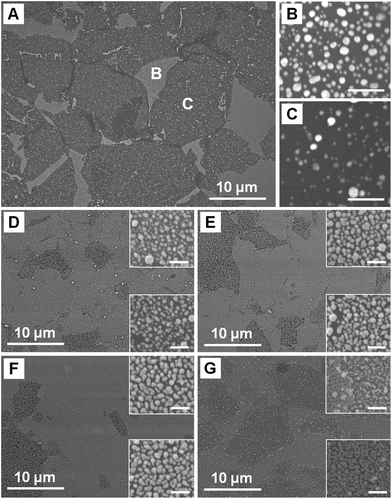 | ||
| Fig. 1 (A) SEM image of Ag NPs formed on rGO films on Si surface at reaction time of 10 s. Magnified SEM images of (B) the exposed Si area and (C) single-layer rGO in (A), scale bars = 200 nm. (D–F) SEM images of Ag NPs formed on rGO films on Si surface at reaction time of 30, 60 and 120 s, respectively. (G) SEM image of Au NPs formed on rGO films on Si surface at reaction time of 30 s. Insets in (D–G) show the magnified images of the NPs formed on exposed Si area (top) and rGO (bottom), scale bars = 200 nm. | ||
The adsorption abilities of different kinds of aromatic molecules on rGO were investigated. The rGO-covered Si wafers can be coated with R6G, MV, RB or MB by immersing the wafers into the respective aqueous solutions (400 μM) for 1 h. The AFM images show that the height of rGO increased from 1.1 to 1.8 nm (Fig. S1 in Electronic supplementary information, ESI†), confirming that R6G was successively adsorbed onto rGO sheets, due to the π–π interaction between R6G and rGO.35 Similarly, MV, RB and MB can also be efficiently adsorbed on rGO sheets (data not shown here).
The as-fabricated Ag NP-decorated rGO film on Si, referred to as Ag NPs-rGO/Si, was used as a SERS substrate for the aforementioned aromatic molecules. The Raman intensities of R6G, MV and RB on bare rGO adsorbed on Si surface, referred to as rGO/Si, are hardly observed, in contrast to the strong Raman signals on the Ag NPs-rGO/Si surface (Fig. 2A–C), indicating the significant role of Ag NPs on the dramatic Raman enhancement. In addition, the strong fluorescence of R6G, MV and RB on Si was observed (Fig. 2A–C). Therefore, the exact enhancement is difficult to be determined. However, the Raman signal of MB on rGO/Si was identified (Fig. 2D), allowing us to determine the enhancement of the fabricated SERS substrate.
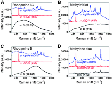 | ||
| Fig. 2 Raman spectra of (A) R6G, (B) MV, (C) RB and (D) MB on Si, rGO/Si and Ag NPs-rGO/Si substrates. | ||
The MB molecules were adsorbed on the exposed rGO region and Ag NPs on Ag NPs-rGO/Si, due to the π–π interaction and covalent bonding,51 respectively. Based on the Raman band of MB at 1625 cm−1, the Raman intensity increases 350 times on the Ag NPs-rGO/Si substrate compared to that on rGO/Si (Fig. 2D), confirming the significant role of Ag NPs on the Raman enhancement of the fabricated SERS substrate. Similarly, the Raman signals of the three other molecules (R6G, MV and RB), which do not adsorb efficiently on Ag,14 are also dramatically enhanced on the Ag NPs-rGO/Si substrates (Fig. 2A–C). These results proved the ability of Ag NPs-rGO/Si to enhance the Raman signal of aromatic molecules, which in general is not adsorbed efficiently on the plasmonic metals.
Furthermore, Raman intensity of the adsorbed molecules varies with the Ag NP size, which is easily controlled by the reaction time when rGO/Si is immersed into a mixed solution of HF and AgNO348–50 (Fig. 3). As the size of Ag NPs increases with the reaction time, the gaps between Ag NPs become smaller, leading to stronger coupling between NPs.52 At the beginning, Raman intensity of R6G increases with the size increase of Ag NPs, due to the stronger coupling between the NPs. The Raman intensity of R6G on Ag NPs-rGO/Si obtained after 30 s reaction is 6.3 times larger than that on Ag NPs-rGO/Si obtained after 10 s reaction. At 30 s-reaction time, although the area of exposed rGO decreases, the stronger coupling between Ag NPs52 outdoes this drawback and hence the substrate gives larger Raman enhancement. As the reaction time is prolonged, the Raman intensity becomes stable due to the combination effects, i.e. the stronger coupling between Ag NPs and the smaller area of exposed rGO for adsorption of R6G. These results demonstrate the significant role of rGO sheets and Ag NPs, used for the adsorption of aromatic molecules and Raman enhancement, respectively. Besides Ag NPs, Au NPs can also be coated onto single-layer rGO sheets (Fig. 1G) in a similar way, simply by replacement of AgNO3 with HAuCl4 in the electroless deposition procedure. These Au NP-decorated rGO sheets can also be used for highly sensitive Raman detection (data not shown here).
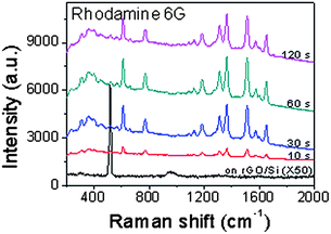 | ||
| Fig. 3 Raman spectra of R6G on rGO/Si and Ag NPs-rGO/Si with Ag NPs formed at reaction time of 10, 30, 60 and 120 s. | ||
Importantly, quantitative detection of R6G, MV, RB and MB can be carried out by using the as-fabricated SERS substrates. The SERS substrates were immersed into aqueous solutions of the aforementioned molecules with different concentrations for 1 h, and subsequently washed with Milli-Q water and dried by N2. Fig. 4 shows that R6G, MV, RB and MB can be detected on Ag NPs-rGO/Si SERS substrates even at a low concentration. For example, the Raman signal of R6G could be detected at a concentration of 10 nM, but no signal of R6G was observed on rGO/Si even at a concentration of 1 mM. The Raman signals for MV, RB and MB can be detected at concentrations of 10, 1 and 1 nM, respectively, indicating that the as-fabricated SERS substrate can be used to detect molecules with high sensitivity.
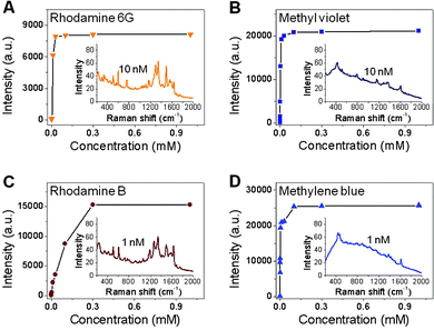 | ||
| Fig. 4 The plots of Raman intensity vs. concentration of (A) R6G, (B) MV, (C) RB and (D) MB, which were adsorbed on Ag NPs-rGO/Si in Fig. 1E. Inset images show Raman spectra of the respective molecules at concentration of 10 nM, 10 nM, 1 nM and 1 nM, respectively. | ||
The Raman enhancement can be further increased by replacing the flat Si substrate with Si nanostructure, e.g.Si nanowells. The Si nanowells were fabricated based on modification of the previous method.48,53 GO sheets were then assembled onto Si nanowells using LB method,46,47 and subsequently reduced to rGO with hydrazine vapour.28,36 The rGO sheets covered the top of Si nanowells (Fig. 5A, B). Based on the band at 1625 cm−1, Raman intensity of adsorbed MB on rGO sheets on Si nanowells increases about 6 times compared to that on rGO/Si (Fig. 5C), demonstrating that Si nanowells can increase the Raman signal of adsorbed molecules, due to the enhanced light absorption, which is consistent with the previous report.54
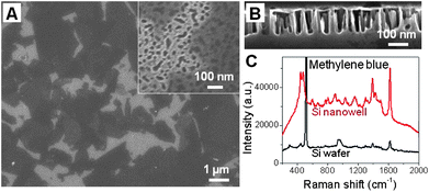 | ||
| Fig. 5 SEM images of (A) top and (B) side view of rGO sheets assembled on Si nanowell substrates. Inset in (A): A magnified top-view image. (C) Raman spectra of adsorbed MB on rGO sheets coated on Si and Si nanowells. | ||
After the rGO-coated Si nanowells were decorated with Ag NPs using the aforementioned method, the Raman signal was further enhanced. The Raman intensities of R6G, MV and RB on Ag NPs-rGO on Si nanowells increased by about 5 times compared to that on Ag NPs-rGO/Si (Fig. 6A–C). As for MB, the Raman enhancement is even higher, ca. 15.9 times (Fig. 6D), since more MB was adsorbed onto Ag NPs via the covalent bonding.51 These results demonstrate that the Ag NP-coated Si nanowells can significantly enhance the Raman signal of adsorbed molecules, due to the enhanced light absorption, which is similar to that on bare Si nanowells, but a much stronger Raman signal was obtained on the Ag NP-rGO on Si nanowells. Therefore, the Ag NPs-rGO on Si nanowells can serve as a more efficient SERS substrate for the detection of molecules, especially for aromatic molecules. Since previous reports demonstrated that DNA and protein can be efficiently adsorbed onto graphene surface,23,55,56 we believe our Ag NPs-rGO on Si or Si nanostructures will have great potential for detection of DNA or protein.
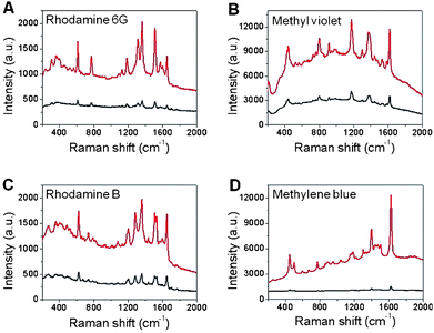 | ||
| Fig. 6 Raman spectra of (A) R6G, (B) MV, (C) RB and (D) MB on Ag NPs-rGO on Si nanowells (upper curves) and Ag NPs-rGO/Si (bottom curves). The reaction time for formation of Ag NPs is 60 s. | ||
Conclusions
A simple, convenient and efficient method is developed to fabricate Ag or Au NP-decorated rGO sheets on Si substrates by electroless deposition, which exhibit strong adsorption of aromatic molecules and dramatic Raman enhancement, owing to the nature of rGO and the deposited Ag or Au NPs, respectively. The adsorbed aromatic molecules are easily detected with high sensitivity. Importantly, the enhancement can be further increased if Si nanostructures are used to replace flat Si substrates. Moreover, our developed SERS substrates might have great potential to detect biomolecules, such as DNA and protein.Experimental section
Materials
Nature graphite (SP-1) was purchased from Bay Carbon (Bay City, MI, USA) and used for synthesizing graphene oxide (GO). 3-Aminopropyltriethoxysilane (APTES), 98% sulfuric acid (H2SO4), 30% hydrogen peroxide (H2O2), potassium permanganate (KMnO4), hydrogen fluoride (40%), silver nitrate (AgNO3, 99.9%), gold(III) chloride trihydate (HAuCl4·3H2O), rhodamine 6G (R6G), rhodamine B (RB), methyl violet (MV) and methylene blue (MB) were purchased from Sigma-Aldrich Pte Ltd (Singapore). Silicon wafers were purchased from Bonda Technology Pte Ltd (Singapore). All chemicals were used as received without further purification. Milli-Q water (Milli-Q System, Millipore, Billerica, MA, USA) was used in all experiments.Preparation of SERS substrates
GO was synthesized from the natural graphite by using the modified Hummers method.36,57 The synthesized GO was re-dispersed in a mixed solution of water and methanol (1![[thin space (1/6-em)]](https://www.rsc.org/images/entities/char_2009.gif) :5), and then assembled on flat Si substrates or Si nanowell substrates using Langmuir–Blodgett (LB) method.46,47 Briefly, a 8–12 mL GO solution was spread onto a water surface in the LB trough at a drop rate of 100 μL min−1. After compression of the GO film on the water surface, a freshly Piranha solution-cleaned Si (or Si nanowell) substrate was vertically dipped into the solution and then slowly pulled up (2 mm min−1) to get a single-layer GO film on the Si. The GO sheets on the Si surface were reduced to obtain reduced graphene oxide (rGO) sheets by hydrazine vapor.28,36,37
:5), and then assembled on flat Si substrates or Si nanowell substrates using Langmuir–Blodgett (LB) method.46,47 Briefly, a 8–12 mL GO solution was spread onto a water surface in the LB trough at a drop rate of 100 μL min−1. After compression of the GO film on the water surface, a freshly Piranha solution-cleaned Si (or Si nanowell) substrate was vertically dipped into the solution and then slowly pulled up (2 mm min−1) to get a single-layer GO film on the Si. The GO sheets on the Si surface were reduced to obtain reduced graphene oxide (rGO) sheets by hydrazine vapor.28,36,37
The rGO-covered Si substrate was immersed in a mixed aqueous solution of HF (2%) and AgNO3 (4 mM) for 15 s–5 min to synthesize a layer of Ag nanoparticles (NPs) onto the rGO and exposed Si surface.49 The size and distance of Ag NPs could be easily tuned by varying the reaction time. The Ag NPs can be replaced with Au NPs by simply replacing AgNO3 with HAuCl4 in the reaction mentioned above.
The Si nanowells were fabricated based on modification of previously reported method.48,53 Briefly, Ag NPs, deposited by immersing a Si substrate in a mixed aqueous solution of HF (1%) and AgNO3 (2 mM) for 60 s, were used as catalyst for the subsequent etching of Si in a mixed solution of H2O2 (0.6%) and HF (5%) to generate Si nanowells. After the single-layer rGO film was assembled onto the Si nanowell substrate using the LB method,46,47 it was decorated with Ag NPs using the aforementioned electroless deposition method.
The R6G, MV, RB and MB were adsorbed onto the as-fabricated SERS substrates by immersing the 10 mm × 6 mm SERS substrates in 1 mL of the respective aqueous solutions (400 μM) for 1 h. The substrates were then thoroughly washed with Milli-Q water and subsequently dried with N2. The bulky samples of R6G, MV, RB and MB powder on Si were measured by Raman spectroscopy and used for control experiments.
Characterization of SERS substrates
Scanning electron microscopy (SEM) was performed using a JEOL JSM-6340F field-emission scanning electron microanalyzer at an accelerating voltage of 5 kV. AFM images were obtained by using Dimension 3100 (Veeco, Santa Barbara, CA, USA) in tapping mode with a Si tip (Tap300-Al, Budget Sensor, spring constant: 42 N m−1, resonant frequency: 320 kHz) under ambient conditions. The Raman detection was carried out on a WITec CRM200 confocal Raman microscopy system with excitation of 633 nm and an air-cooled charge coupled device (CCD) as the detector (WITec Instruments Corp, Germany). The Raman band of a silicon wafer at 520 cm−1 was used as a reference to calibrate the spectrometer.Acknowledgements
This work was supported by AcRF Tier 2 (ARC 10/10, No. MOE2010-T2-1-060) from MOE, CREATE program (Nano-materials for Energy and Water Management) from NRF, and New Initiative Fund FY 2010 (M58120031) from NTU in Singapore.Notes and references
- A. Campion and P. Kambhampati, Chem. Soc. Rev., 1998, 27, 241–250 RSC
.
- G. A. Baker and D. S. Moore, Anal. Bioanal. Chem., 2005, 382, 1751–1770 CrossRef CAS
- C. L. Haynes, C. R. Yonzon, X. Y. Zhang and R. P. Van Duyne, J. Raman Spectrosc., 2005, 36, 471–484 CrossRef CAS
- M. Moskovits, J. Raman Spectrosc., 2005, 36, 485–496 CrossRef CAS
- P. L. Stiles, J. A. Dieringer, N. C. Shah and R. R. Van Duyne, Annu. Rev. Anal. Chem., 2008, 1, 601–626 CrossRef CAS
- L. D. Qin, S. L. Zou, C. Xue, A. Atkinson, G. C. Schatz and C. A. Mirkin, Proc. Natl. Acad. Sci. U. S. A., 2006, 103, 13300–13303 CrossRef CAS
- M. J. Banholzer, J. E. Millstone, L. D. Qin and C. A. Mirkin, Chem. Soc. Rev., 2008, 37, 885–897 RSC
- H. Ko, S. Singamaneni and V. V. Tsukruk, Small, 2008, 4, 1576–1599 CrossRef CAS
- S. Lal, N. K. Grady, J. Kundu, C. S. Levin, J. B. Lassiter and N. J. Halas, Chem. Soc. Rev., 2008, 37, 898–911 RSC
- F. Le, D. W. Brandl, Y. A. Urzhumov, H. Wang, J. Kundu, N. J. Halas, J. Aizpurua and P. Nordlander, ACS Nano, 2008, 2, 707–718 CrossRef CAS
- C. Liusman, S. Z. Li, X. D. Chen, W. Wei, H. Zhang, G. C. Schatz, F. Boey and C. A. Mirkin, ACS Nano, 2010, 4, 7676–7682 CrossRef CAS
- S. J. Lee, Z. Q. Guan, H. X. Xu and M. Moskovits, J. Phys. Chem. C, 2007, 111, 17985–17988 CAS
- K. Hering, D. Cialla, K. Ackermann, T. Dorfer, R. Moller, H. Schneidewind, R. Mattheis, W. Fritzsche, P. Rosch and J. Popp, Anal. Bioanal. Chem., 2008, 390, 113–124 CrossRef CAS
- J. W. Zheng, X. W. Li, R. N. Gu and T. H. Lu, J. Phys. Chem. B, 2002, 106, 1019–1023 CrossRef CAS
- K. S. Novoselov, A. K. Geim, S. V. Morozov, D. Jiang, Y. Zhang, S. V. Dubonos, I. V. Grigorieva and A. A. Firsov, Science, 2004, 306, 666–669 CrossRef CAS
- Y. B. Zhang, Y. W. Tan, H. L. Stormer and P. Kim, Nature, 2005, 438, 201–204 CrossRef CAS
- P. Avouris, Z. H. Chen and V. Perebeinos, Nat. Nanotechnol., 2007, 2, 605–615 CrossRef CAS
- A. K. Geim and K. S. Novoselov, Nat. Mater., 2007, 6, 183–191 CrossRef CAS
- F. Bonaccorso, Z. Sun, T. Hasan and A. C. Ferrari, Nat. Photonics, 2010, 4, 611–622 CrossRef CAS
- F. Schwierz, Nat. Nanotechnol., 2010, 5, 487–496 CrossRef CAS
- X. Huang, Z. Y. Yin, S. X. Wu, X. Y. Qi, Q. Y. He, Q. C. Zhang, Q. Y. Yan, F. Boey and H. Zhang, Small, 2011 DOI:10.1002/smll.201002009
- A. K. Geim, Science, 2009, 324, 1530–1534 CrossRef CAS
- N. Varghese, U. Mogera, A. Govindaraj, A. Das, P. K. Maiti, A. K. Sood and C. N. R. Rao, ChemPhysChem, 2009, 10, 206–210 CrossRef CAS
- K. P. Loh, Q. L. Bao, G. Eda and M. Chhowalla, Nat. Chem., 2010, 2, 1015–1024 CrossRef CAS
-
(a) Z. J. Wang, X. Z. Zhou, J. Zhang, F. Boey and H. Zhang, J. Phys. Chem. C, 2009, 113, 14071–14075 CrossRef CAS
-
(a) Q. Y. He, H. G. Sudibya, Z. Y. Yin, S. X. Wu, H. Li, F. Boey, W. Huang, P. Chen and H. Zhang, ACS Nano, 2010, 4, 3201–3208 CrossRef CAS
- B. Li, X. H. Cao, H. G. Ong, J. W. Cheah, X. Z. Zhou, Z. Y. Yin, H. Li, J. L. Wang, F. Boey, W. Huang and H. Zhang, Adv. Mater., 2010, 22, 3058–3061 CrossRef CAS
- X. Z. Zhou, Y. Y. Wei, Q. Y. He, F. Boey, Q. C. Zhang and H. Zhang, Chem. Commun., 2010, 46, 6974–6976 RSC
- X. H. Cao, Q. Y. He, W. H. Shi, B. Li, Z. Y. Zeng, Y. M. Shi, Q. Y. Yan and H. Zhang, Small, 2011, 7, 1199–1202 CrossRef CAS
- H. G. Sudibya, Q. Y. He, H. Zhang and P. Chen, ACS Nano, 2011, 5, 1990–1994 CrossRef CAS
-
(a) J. Q. Liu, Z. Y. Yin, X. H. Cao, F. Zhao, A. P. Lin, L. H. Xie, Q. L. Fan, F. Boey, H. Zhang and W. Huang, ACS Nano, 2010, 4, 3987–3992 CrossRef CAS
- Z. Y. Yin, S. X. Wu, X. Z. Zhou, X. Huang, Q. C. Zhang, F. Boey and H. Zhang, Small, 2010, 6, 307–312 CrossRef CAS
-
(a) Z. Y. Yin, S. Y. Sun, T. Salim, S. X. Wu, X. A. Huang, Q. Y. He, Y. M. Lam and H. Zhang, ACS Nano, 2010, 4, 5263–5268 CrossRef CAS
- S. Agarwal, X. Zhou, F. Ye, Q. He, G. C. K. Chen, F. Boey, H. Zhang and P. Chen, Langmuir, 2010, 26, 2244–2247 CrossRef CAS
- X. Ling, L. M. Xie, Y. Fang, H. Xu, H. L. Zhang, J. Kong, M. S. Dresselhaus, J. Zhang and Z. F. Liu, Nano Lett., 2010, 10, 553–561 CrossRef CAS
- X. Z. Zhou, X. Huang, X. Y. Qi, S. X. Wu, C. Xue, F. Y. C. Boey, Q. Y. Yan, P. Chen and H. Zhang, J. Phys. Chem. C, 2009, 113, 10842–10846 CAS
- D. Li, M. B. Muller, S. Gilje, R. B. Kaner and G. G. Wallace, Nat. Nanotechnol., 2008, 3, 101–105 CrossRef CAS
- A. N. Obraztsov, E. A. Obraztsova, A. V. Tyurnina and A. A. Zolotukhin, Carbon, 2007, 45, 2017–2021 CrossRef CAS
- A. Reina, X. T. Jia, J. Ho, D. Nezich, H. B. Son, V. Bulovic, M. S. Dresselhaus and J. Kong, Nano Lett., 2009, 9, 30–35 CrossRef CAS
- D. C. Wei, Y. Q. Liu, Y. Wang, H. L. Zhang, L. P. Huang and G. Yu, Nano Lett., 2009, 9, 1752–1758 CrossRef CAS
- R. Pasricha, S. Gupta and A. K. Srivastava, Small, 2009, 5, 2253–2259 CrossRef CAS
- X. Q. Fu, F. L. Bei, X. Wang, S. O'Brien and J. R. Lombardi, Nanoscale, 2010, 2, 1461–1466 RSC
- K. Jasuja, J. Linn, S. Melton and V. Berry, J. Phys. Chem. Lett., 2010, 1, 1853–1860 CrossRef CAS
- Y. K. Kim, H. K. Na, Y. W. Lee, H. Jang, S. W. Han and D. H. Min, Chem. Commun., 2010, 46, 3185–3187 RSC
- J. Li and C. Y. Liu, Eur. J. Inorg. Chem., 2010, 1244–1248 CrossRef CAS
- L. J. Cote, F. Kim and J. X. Huang, J. Am. Chem. Soc., 2009, 131, 1043–1049 CrossRef CAS
- G. Lu, X. Z. Zhou, H. Li, Z. Y. Yin, B. Li, L. Huang, F. Boey and H. Zhang, Langmuir, 2010, 26, 6164–6166 CrossRef CAS
-
(a) K. Q. Peng, J. J. Hu, Y. J. Yan, Y. Wu, H. Fang, Y. Xu, S. T. Lee and J. Zhu, Adv. Funct. Mater., 2006, 16, 387–394 CrossRef CAS
- K. Q. Peng, A. J. Lu, R. Q. Zhang and S. T. Lee, Adv. Funct. Mater., 2008, 18, 3026–3035 CrossRef CAS
- B. H. Zhang, H. S. Wang, L. H. Lu, K. L. Ai, G. Zhang and X. L. Cheng, Adv. Funct. Mater., 2008, 18, 2348–2355 CrossRef CAS
- G. N. Xiao and S. Q. Man, Chem. Phys. Lett., 2007, 447, 305–309 CrossRef CAS
- Z. H. Zhu, T. Zhu and Z. F. Liu, Nanotechnology, 2004, 15, 357–364 CrossRef CAS
- T. Qiu and P. K. Chu, Mater. Sci. Eng., R, 2008, 61, 59–77 CrossRef
- G. Fan, H. Zhu, K. Wang, J. Wei, X. Li, Q. Shu, N. Guo and D. Wu, ACS Appl. Mater. Interfaces, 2011, 3, 721–725 CAS
- S. Mao, G. H. Lu, K. H. Yu, Z. Bo and J. H. Chen, Adv. Mater., 2010, 22, 3521–3526 CrossRef CAS
- J. F. Shen, M. Shi, B. Yan, H. W. Ma, N. Li, Y. Z. Hu and M. X. Ye, Colloids Surf., B, 2010, 81, 434–438 CrossRef CAS
- X. Z. Zhou, G. Lu, X. Y. Qi, S. X. Wu, H. Li, F. Boey and H. Zhang, J. Phys. Chem. C, 2009, 113, 19119–19122 CAS
Footnote |
| † Electronic supplementary information (ESI) available: AFM images of rGO sheets on Si substrate before (A) and after (B) adsorption of R6G. See DOI: 10.1039/c1sc00254f |
| This journal is © The Royal Society of Chemistry 2011 |