Nanoparticle SERS substrates with 3D Raman-active volumes
Kelsey A.
Stoerzinger
a,
Julia Y.
Lin
b and
Teri W.
Odom
*ab
aDepartment of Material Science and Engineering, Northwestern University, Evanston, IL 60208-3113, USA. E-mail: todom@northwestern.edu
bDepartment of Chemistry, Northwestern University, Evanston, IL 60208-3113, USA
First published on 6th May 2011
Abstract
This Perspective reviews a new class of surface-enhanced Raman scattering (SERS) nanoparticle substrates defined by their three-dimensional (3D) confinement of localized electromagnetic fields. First, we describe the critical design parameters and recent advances in nanofabrication to create reproducible nanoparticle assemblies for SERS. Next, we highlight a promising platform—gold nanopyramids—for testing how the local arrangement of particles in an assembly affects the overall SERS response. The dimensions and optical properties of the nanopyramids can be tuned easily, and their unique anisotropic shape allows them to be organized into different particle configurations with 3D Raman-active volumes. Because of their large hot-spot volumes, this unique class of nanoparticle substrates offers an attractive alternative for ultra-sensitive sensors and trace chemical analysis.
Introduction
Surface enhanced Raman scattering (SERS) is a surface-sensitive, vibrational phenomena characterized by increased Raman scattering from molecules that are situated on or near roughened metal surfaces and metal nanostructures.1–3 Enhanced Raman scattering was first observed on uneven metal films with regions of high curvature and gaps between metal grains.4 The confined electromagnetic fields, commonly referred to as “hot spots,”5 were believed to originate from localized surface plasmons (LSPs) excited in these areas.1–3,6 Metal nanoparticles (NPs) have generated interest as SERS substrates because they exhibit both tunable LSPs and high radii of curvature that can generate reproducible hot spots.7 Raman enhancement scales with the square of the electromagnetic field intensity8 and is maximized when the LSP resonances of metal nanostructures occur between the excitation and Stokes-shifted wavelength.9For NPs with anisotropic shapes, the electromagnetic fields are most concentrated at asperities (Fig. 1),10–12 such as the apexes of triangles7,13 or the corners of cubes.14 When NPs of the same size and shape are assembled into small clusters, well-defined hot spots form in the nanoscale junctions between them, which increases the SERS response compared to that of a single NP.15,16 The main challenge of using anisotropic or assembled NPs as reproducible SERS substrates is their preparation. Typically, chemically synthesized particles require stabilizing ligands to control their shape and size and to avoid undesired aggregation; however, regulating critical factors, such as the concentration of ligands, purity of precursors and solvents, and uniform reaction temperature, is not trivial. The generation of identical NPs from batch-to-batch remains a challenge. Also, the ligands on solution-synthesized NP surfaces can inhibit the adsorption of Raman reporter molecules.
 | ||
| Fig. 1 Calculated electric field intensities for different metal NP shapes and dimers at LSP resonance wavelengths of (a) nanoprism with hot spots at sharp asperities (top-down), (b) nanoprism dimer (top-down), (c) nanosphere dimer, and (d) two stacked nanopyramids (side-view). Red color corresponds to highest intensity. Adapted with permission from ref. 21 and 32. Copyrights 2004 American Institute of Physics and 2010 American Chemical Society. | ||
Recent advances in NP fabrication and assembly have offered new possibilities to tailor hot spot volumes with reproducible SERS signals.17 Top-down fabrication provides a controlled method to form highly anisotropic structures of relatively large sizes (> 100 nm) with ligand-free surfaces.17,18Assembly and templating techniques can create structures that confine electric fields within the entire region between two parallel metal faces, which we define here as a 3D Raman-active volume.8,19–21 These NP architectures with large-volume hot spots support the greatest average field enhancement rather than the greatest absolute field enhancement (the latter is most important for single molecule detection).22 Hence, NP substrates with 3D Raman-active volumes provide a new mechanism (1) to improve the sensitive detection of trace analytes and (2) to tailor the particle placement in designing hierarchical structures with large hot spot volumes. In the following sections, we will discuss intrinsic factors (particle shape, interparticle separation, and orientation) and extrinsic factors (polarization of light) that are important to optimize SERS and will focus specifically on ordered assemblies of nanocubes, nanodisks, and pyramidal nanoshells.
SERS and nanoparticle dimers: Dependence on shape and gap size
SERS signals can increase when NPs aggregate or are directed into assembled structures because of strong electromagnetic fields confined between particles.16,23–26 NP dimers27,28 are of particular interest for SERS because the electric field intensities within the gap exceed those from hot spots on the surface of an isolated particle.8,16,29–31Fig. 1 shows the calculated electric field distributions of a single particle and various dimers at their respective LSP resonance wavelengths. There are three important parameters in designing NP dimers with localized hot spots: (1) the shape of the constituent particles, (2) the polarization of incident light, and (3) the size of the gap between particles.Dimers composed of anisotropic particles can increase Raman scattering because the sharp features used to define the gap support high electromagnetic field intensities. For example, the field intensity between two triangular prisms oriented tip-to-tip (Fig. 1b) was greater than that between spheres (Fig. 1c) because of the concentration of electromagnetic fields within regions of higher curvature.32 In addition, comparison between dimers of nanocubes and spheres revealed that dimers comprised of cubes were more SERS-active because of the field localization at their corners.15 Besides pairs of smaller (< 100 nm) constituent NPs, dimers of large anisotropic structures, such as nanopyramidal shells (Fig. 1d), also exhibit fields confined at asperities—the tip and the narrow edge at the base of the pyramid—that contribute to a strong SERS response.21
SERS has been shown to depend on the angle θ between the polarization and the dipole moment associated with the excited LSP mode in a cos2θ manner.33 The strongest electromagnetic fields will occur when incident light is polarized parallel to the dimer axis, which promotes coupling between the NPs15,19 and leads to electromagnetic field localization within the gap. Dimers of silver nanocubes demonstrate that this polarization effect did not depend on particle orientation within the assembled structure (Fig. 2).8,19,32,34–37 When two nanocube faces were parallel (face-to-face), the measured Raman signal was over 10 times greater than the case where two nanocubes were oriented edge-to-edge. When the edge of one nanocube was located at the center of a face (edge-to-face), the Raman signal was reduced by ∼ 25% compared to the face-to-face configuration.19 Although the electric field intensity is expected to be highest between two corners,38 the hot spot volume is very small. Hence, the greater enhancement from dimers with parallel faces is a result of a greater number of molecules contained in the large hot spot.19
 | ||
| Fig. 2 Nanocube dimers oriented face-to-face generate SERS intensity higher than other dimer configurations. The polarization is along the dimer axis of 100-nm silver particles, and the Raman reporter molecule was 4-methylbenzenethiol. Reprinted with permission from ref. 19. Copyright 2010 Elsevier B.V. | ||
Most previous work has suggested that nanoscale (1–2 nm) gaps were required for optimized Raman enhancement28,29,35,39–42 because the dimension of the gap within a NP dimer strongly influences the intensity and distribution of the electromagnetic fields. Unexpectedly, however, higher SERS responses have been observed from large (10–30 nm) gap distances defined by large (>150 nm) nanostructures. The systematic investigation of large particle dimers has been enabled by novel fabrication routes that offer control over the material, shape, and thickness of the constituent particles8,20,21,43,44 so that specific geometric parameters can be correlated with the resulting Raman signal. For example, NP dimers can be formed by depositing alternating layers of gold and a sacrificial material within a template and then etching the spacer metal to produce well-defined gaps.8,20
Dimers of gold disks (d = 360 nm) that were relatively thick (120 nm) and separated by large (up to 30 nm) distances produced SERS signals and field intensities (Fig. 3a)8 comparable to NP substrates with gaps on the order of several nanometres. We also found a similar result for dimers comprised of two pyramidal nanoshells (d = 300 nm and 20-nm gold shell thickness).20 In the latter case, the size of the gap between the nested shells was varied by the amount of spacer layer that was etched away. Chromium was chosen as the sacrificial material because we could judiciously control the etch rates. A shorter etch time led to a large gap (30 nm) between pyramidal shells, which supported a SERS signal 60 times higher than when the sacrificial layer was etched away completely, and where the inner and outer pyramidal shells collapsed to form a very small gap (5 nm) (Fig. 3b, c).20
 | ||
| Fig. 3 Fabricated dimers with large hot-spot volumes. (a) SEM image of Au disk (120-nm thick) dimers separated by (bottom left to top right) 160, 80, 30, 15, and 5 nm gaps, and corresponding Raman image. (b) SEM image of two nested Au nanopyramids with a 5-nm gap and no appreciable Raman signal. (c) SEM of nested Au nanopyramids with a 30-nm gap and a strong Raman signal. All Raman images were acquired at the 1624 cm−1 band of methylene blue with a 633-nm HeNe laser. Adapted with permission from ref. 8 and 20. Copyrights 2006 National Academy of Sciences, USA and 2010 American Chemical Society. | ||
Tailoring 3D Raman-active volumes using pyramidal nanoshell dimers
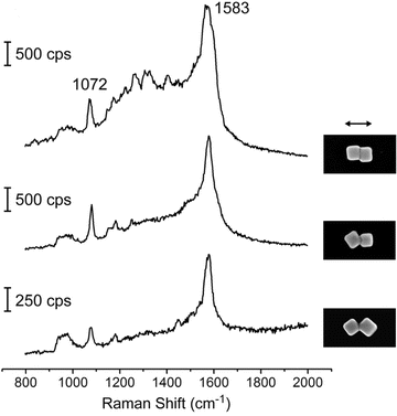
Nanofabricated pyramidal nanoshells are ideal SERS substrates because (1) the dimensions and plasmon resonances of these particles can be easily tuned;45,46 and (2) their anisotropic shape allows them to be assembled into different particle configurations with large Raman-active volumes. Fig. 4 compares the SERS response of the pyramidal nanoshell dimers with two different arrangements: side-to-side and stacked. Side-to-side assemblies were characterized by an outer face of one pyramid being nearly parallel with that of a neighboring pyramid (Fig. 4a). In contrast, stacked assemblies consisted of four parallel faces since one pyramidal shell was embedded within the other. Both the stacked and side-to-side dimers of pyramidal nanoshells produced greater SERS signals compared to the response from a single particle (or two single particles). | ||
| Fig. 4 Stacked nanopyramid dimers produce a SERS response larger than side-to-side dimers. (a) 3D illustration and SEM of a single particle, a side-to-side dimer, and a stacked dimer. All images are 1.5 μm × 1.5 μm; the Au shell thickness was 20 nm. (b) Corresponding Raman spectra for nanopyramid dimers in (a) coated with a monolayer of methylene blue molecules excited by 633-nm laser light. Adapted with permission from ref. 21. Copyright 2010 American Chemical Society. | ||
Although FDTD modeling showed high field intensities at the tips and edges of the pyramidal shells, a large region of comparable field strength was located within the gap between the particles (Fig. 1d).21 Comparison of stacked and side-to-side pyramids revealed that the stacked structure generated a SERS signal over four times greater than the side-to-side dimer. This increase in signal most likely corresponds to the 4-fold increase in the number of parallel faces within the assembly. The effective increase in the size of the hot spot volume allowed a higher concentration of molecules to contribute to the SERS response. Thus, by tailoring the geometry of the Raman-active volume, the hot spot can be manipulated to optimize SERS.19,47
Enhancing SERS with pyramidal nanoshell trimers
The 3D geometry of the nanopyramids enables the formation of higher-order, 3D assemblies. By taking advantage of this unique structural parameter, we expanded the investigation of Raman-active volumes from dimers to trimers in order to achieve additional insight into the design of optimal NP SERS substrates. A pyramidal nanoshell stacked within another particle in a side-to-side pair, a “mixed” trimer, produced a signal ∼ 2.5 times greater than that of three side-to-side pyramids (Fig. 5). This increase in signal can be attributed to the “mixed” trimer having a larger (2.5 times) SERS-active volume than the side-to-side trimer. Similar results were observed in stacked trimers, where the signal was ten times larger than that of a side-to-side trimer; the hot spot volume available in stacked pyramids was four times larger than that of the side-to-side assemblies. Therefore, the local arrangement of NPs within a cluster can now be considered a new and critical parameter in the design of optimal SERS NP substrates.21 Combined with polarization, gap spacing, and shape of constituent particles, the relative orientation of anisotropic NPs provides an additional means to increase SERS signals.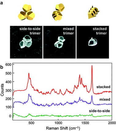 | ||
| Fig. 5 Stacked nanopyramid trimers produce a SERS response larger than other nanopyramid trimers. (a) 3D illustrations and SEM images of different trimer configurations. All images are 1.5 μm × 1.5 μm; the Au shell thickness was 20 nm. (b) Corresponding Raman spectra for nanopyramid trimers in (a) coated with a monolayer of methylene blue molecules excited by 633-nm laser light. Adapted with permission from ref. 21. Copyright 2010 American Chemical Society. | ||
Conclusions and future outlook
This Perspective highlighted NP SERS substrates that supported 3D Raman-active volumes. We identified several critical design parameters, such as particle size, particle shape, and interparticle separation, needed to create reproducible SERS substrates. We discussed how signal was maximized for dimers of large anisotropic NPs with hot spots defined by parallel metallic faces separated by large gap distances (>10 nm). Access to these types of structures is now possible because of new fabrication and assembly methods. Because NPs such as nanopyramids support high electric field intensities over a large (50,000 nm3) volume, they mitigate the challenge of directing molecular adsorption to a nanoscale hot spot (e.g. one defined between adjacent tips). Hence, hot spot volumes defined by parallel NP faces offer an alternative approach to increase SERS signals on NP substrates in sensing applications, especially for trace analytes.Acknowledgements
This work was supported, in part, by the MRSEC program of the National Science Foundation (DMR-0520513) at the Materials Research Center of Northwestern University, the NSF NSEC program at Northwestern University (EEC-0647560), the David and Lucile Packard Foundation, and the NIH Director's Pioneer Award (DP1OD003899). This work used the NUANCE Center facilities, which are supported by NSF-MRSEC, NSF-NSEC, and the Keck Foundation.References
- G. Albrecht and A. Creighton, J. Am. Chem. Soc., 1977, 99, 5215–5217 CrossRef CAS.
- D. L. Jeanmaire and R. P. Van Duyne, J. Electroanal. Chem., 1977, 84, 1–20 CrossRef CAS.
- M. Moskovits, J. Chem. Phys., 1978, 69, 4159–4161 CrossRef CAS.
- M. Fleischmann, P. J. Hendra and A. J. McQuillan, Chem. Phys. Lett., 1974, 26, 163–166 CrossRef CAS.
- T. Jensen, L. Kelly, A. Lazarides and G. C. Schatz, J. Cluster Sci., 1999, 10, 295–317 CrossRef CAS.
- J. Gersten and A. Nitzan, J. Chem. Phys., 1980, 73, 3023–3037 CrossRef CAS.
- K. L. Kelly, E. Coronado, L. L. Zhao and G. C. Schatz, J. Phys. Chem. B, 2002, 107, 668–677.
- L. Qin, S. Zou, C. Xue, A. Atkinson, G. C. Schatz and C. A. Mirkin, Proc. Natl. Acad. Sci. U. S. A., 2006, 103, 13300–13303 CrossRef CAS.
- A. D. McFarland, M. A. Young, J. A. Dieringer and R. P. Van Duyne, J. Phys. Chem. B, 2005, 109, 11279–11285 CrossRef CAS.
- N. Pazos-Pérez, S. Barbosa, L. Rodríguez-Lorenzo, P. Aldeanueva-Potel, J. Pérez-Juste, I. Pastoriza-Santos, R. A. Alvarez-Puebla and L. M. Liz-Marzán, J. Phys. Chem. Lett., 2009, 1, 24–27 Search PubMed.
- G. Duan, W. Cai, Y. Luo, Z. Li and Y. Li, Appl. Phys. Lett., 2006, 89, 211905 CrossRef.
- M. J. Mulvihill, X. Y. Ling, J. Henzie and P. Yang, J. Am. Chem. Soc., 2009, 132, 268–274 Search PubMed.
- L. J. Sherry, R. Jin, C. A. Mirkin, G. C. Schatz and R. P. Van Duyne, Nano Lett., 2006, 6, 2060–2065 CrossRef CAS.
- L. J. Sherry, S.-H. Chang, G. C. Schatz, R. P. Van Duyne, B. J. Wiley and Y. Xia, Nano Lett., 2005, 5, 2034–2038 CrossRef CAS.
- M. Rycenga, P. H. C. Camargo, W. Li, C. H. Moran and Y. Xia, J. Phys. Chem. Lett., 2010, 1, 696–703 Search PubMed.
- R. Alvarez-Puebla, L. M. Liz-Marzán and F. J. García de Abajo, J. Phys. Chem. Lett., 2010, 1, 2428–2434 Search PubMed.
- M. J. Banholzer, J. E. Millstone, L. Qin and C. A. Mirkin, Chem. Soc. Rev., 2008, 37, 885–897 RSC.
- J. Henzie, J. Lee, M. H. Lee, W. Hasan and T. W. Odom, Annu. Rev. Phys. Chem., 2009, 60, 147–165 CrossRef CAS.
- P. H. C. Camargo, L. Au, M. Rycenga, W. Li and Y. Xia, Chem. Phys. Lett., 2010, 484, 304–308 Search PubMed.
- J. Y. Lin, W. Hasan, J.-C. Yang and T. W. Odom, J. Phys. Chem. C, 2010, 114, 7432–7435 Search PubMed.
- K. A. Stoerzinger, W. Hasan, J. Y. Lin, A. Robles and T. W. Odom, J. Phys. Chem. Lett., 2010, 1, 1046–1050 Search PubMed.
- H. Xu, J. Aizpurua, M. Käll and P. Apell, Phys. Rev. E: Stat. Phys., Plasmas, Fluids, Relat. Interdiscip. Top., 2000, 62, 4318–4324 CrossRef CAS.
- M. Moskovits, Rev. Mod. Phys., 1985, 57, 783–826 CrossRef CAS.
- J. P. Camden, J. A. Dieringer, Y. Wang, D. J. Masiello, L. D. Marks, G. C. Schatz and R. P. Van Duyne, J. Am. Chem. Soc., 2008, 130, 12616–12617 CrossRef CAS.
- W. Li, P. H. C. Camargo, L. Au, Q. Zhang, M. Rycenga and Y. Xia, Angew. Chem., Int. Ed., 2010, 49, 164–168 CAS.
- W. Li, P. H. C. Camargo, X. Lu and Y. Xia, Nano Lett., 2008, 9, 485–490.
- J. Aizpurua, G. W. Bryant, L. J. Richter, F. J. García de Abajo, B. K. Kelley and T. Mallouk, Phys. Rev. B: Condens. Matter Mater. Phys., 2005, 71, 235420 CrossRef.
- I. Romero, J. Aizpurua, G. W. Bryant and F. J. García De Abajo, Opt. Express, 2006, 14, 9988–9999 CrossRef.
- J. McMahon, A.-I. Henry, K. Wustholz, M. Natan, R. Freeman, R. Van Duyne and G. Schatz, Anal. Bioanal. Chem., 2009, 394, 1819–1825 CrossRef CAS.
- R. G. Freeman, K. C. Grabar, K. J. Allison, R. M. Bright, J. A. Davis, A. P. Guthrie, M. B. Hommer, M. A. Jackson, P. C. Smith, D. G. Walter and M. J. Natan, Science, 1995, 267, 1629–1632 CrossRef CAS.
- P. K. Aravind, A. Nitzan and H. Metiu, Surf. Sci., 1981, 110, 189–204 CrossRef CAS.
- E. Hao and G. C. Schatz, J. Chem. Phys., 2004, 120, 357–366 CrossRef CAS.
- P. G. Etchegoin, C. Galloway and E. C. Le Ru, Phys. Chem. Chem. Phys., 2006, 8, 2624–2628 RSC.
- S. Y. Lee, L. Hung, G. S. Lang, J. E. Cornett, I. D. Mayergoyz and O. Rabin, ACS Nano, 2010, 4, 5763–5772 Search PubMed.
- C. E. Talley, J. B. Jackson, C. Oubre, N. K. Grady, C. W. Hollars, S. M. Lane, T. R. Huser, P. Nordlander and N. J. Halas, Nano Lett., 2005, 5, 1569–1574 CrossRef CAS.
- D.-S. Kim, J. Heo, S.-H. Ahn, S. W. Han, W. S. Yun and Z. H. Kim, Nano Lett., 2009, 9, 3619–3625 CrossRef CAS.
- P. H. C. Camargo, M. Rycenga, L. Au and Y. Xia, Angew. Chem., Int. Ed., 2009, 48, 2180–2184 CrossRef CAS.
- J. M. McLellan, Z.-Y. Li, A. R. Siekkinen and Y. Xia, Nano Lett., 2007, 7, 1013–1017 CrossRef CAS.
- H. Wang, C. S. Levin and N. J. Halas, J. Am. Chem. Soc., 2005, 127, 14992–14993 CrossRef CAS.
- Y. Sawai, B. Takimoto, H. Nabika, K. Ajito and K. Murakoshi, J. Am. Chem. Soc., 2007, 129, 1658–1662 CrossRef CAS.
- T. Atay, J.-H. Song and A. V. Nurmikko, Nano Lett., 2004, 4, 1627–1631 CrossRef CAS.
- H. Xu and M. Käll, Phys. Rev. Lett., 2002, 89, 246802 CrossRef.
- M. J. Banholzer, S. Li, J. B. Ketter, D. I. Rozkiewicz, G. C. Schatz and C. A. Mirkin, J. Phys. Chem. C, 2008, 112, 15729–15734 CrossRef CAS.
- S. Li, M. L. Pedano, S.-H. Chang, C. A. Mirkin and G. C. Schatz, Nano Lett., 2010, 10, 1722–1727 CrossRef CAS.
- J. Henzie, E.-S. Kwak and T. W. Odom, Nano Lett., 2005, 5, 1199–1202 Search PubMed.
- J. Lee, W. Hasan, C. L. Stender and T. W. Odom, Acc. Chem. Res., 2008, 41, 1762–1771 CrossRef CAS.
- P. H. C. Camargo, C. M. Cobley, M. Rycenga and Y. Xia, Nanotechnology, 2009, 20, 434020 CrossRef.
| This journal is © The Royal Society of Chemistry 2011 |