Electrodeposition as a superior route to a thin film molecular semiconductor†
Simon
Dalgleish
a,
Hirofumi
Yoshikawa
b,
Michio M.
Matsushita
b,
Kunio
Awaga
b and
Neil
Robertson
*a
aSchool of Chemistry and EaSTCHEM Research School, University of Edinburgh, West Mains Road, Edinburgh, UK EH9 3JJ. E-mail: neil.robertson@ed.ac.uk
bResearch Center of Materials Science, Nagoya University, Chikusa-ku, Nagoya, 464-8602, Japan
First published on 29th October 2010
Abstract
Electrooxidation to form neutral films of a homoleptic nickel dithiolene [Ni(b-3ted)2] (1) from an air-stable TBA salt is described [b-3ted = bis(3-thienyl)-1,2-ethylenedithiolene; TBA = tetrabutylammonium]. Films grown by potentiostatic electrodeposition directly onto interdigitated electrode arrays show improved conductivity compared to those formed by solution methods. The grown films are free from residual electrolyte doping, and this technique is shown to yield robust films of reproducible electronic performance. The conductivity of films formed by electrodeposition show gate dependence when grown directly onto field effect transistor substrates. Thin-film X-ray diffraction confirms the electrodeposited films to be of the same polymorph as films and single crystals formed by solution methods. Scanning electron microscopy shows the electrodeposited films to have larger, more connected polycrystalline regions, as well as improved contact with the electrodes.
1 Introduction
Film formation by solution methods, such as drop and spin coating, have been used very successfully to develop high quality films.1–3 However, the suitability of such techniques is reliant on the solubility of the material in question. One major obstacle to the development of molecular electronics is often the poor solubility of the materials. Whilst it is a goal for synthetic chemists to develop materials with a large degree of molecular interaction, such as π-stacking, this inevitably leads to their reduced solubility. As a result, assessing the performance of the material in practical devices, such as field effect transistors (FETs), becomes difficult. For particularly insoluble systems, vapour techniques, such as physical vapour deposition (PVD) and chemical vapour deposition (CVD), can form high quality films.4,5 However, such techniques are performed under high vacuum conditions, and as such are unsuitable for large-scale device fabrication, due to the huge costs of evacuating large volumes.Square-planar metal bis-dithiolenes are attractive materials for electronic application, due to their multiple stable redox states, and their highly planar molecular geometry, allowing for extensive intermolecular interaction.6 However they present an interesting problem for device incorporation: their boiling point is often too high, or thermal stability too low for sublimation,4 and without deliberate structural modification, their solubility is often too low for effective solution processing.7 As a result, other alternative methods for processing neutral metal dithiolene films, in a cheap and reproducible manner, are of great interest in materials chemistry.
Electrodeposition is a technique whereby a material can be deposited on a conducting electrode from solution by the change of its redox state, and may be a potential solution to this problem.8 In the case of dithiolenes, their multiple stable redox states mean that salts, often with greatly improved solubility, can be isolated easily. Under electro-oxidative conditions, these salts may be oxidised to the less soluble neutral species, and thus deposit on a conducting electrode. This technique is not limited to dithiolenes, as salts of many common semiconductors can be formed, often with much higher solubility than the neutral species.
Electrodeposition of dithiolenes has previously been investigated by some groups as a route to thin films.9–11 However, in all reported examples of dithiolene electrodeposition, at least some level of residual ionic species was observed in the film following electrodeposition. Indeed, it was this residual ion doping that in some cases led to their investigation as gas sensors.11
During the course of a previous investigation into the electropolymerisation of [Ni(b-3ted)2] (1),12 we observed that, on cycling [1][TBA] to potentials sufficient to oxidise [1]−1 to 1 (+0.29 V vs.SCE), a film formed on the working electrode that was thought to be molecular, due to its complete solubility in DCM, and identical UV/Vis/NIR absorption spectra in solution, compared to 1. From this study, it seemed that the insolubility of 1 in MeCN, compared to the monoanion, resulted in it being controllably deposited on the working electrode.
In this study we compare the properties of such films of 1, formed by electrodeposition (1a), to those formed by a more conventional pseudo-drop casting method (1b), and demonstrate electrodeposition as an alternative means for the formation of semiconductive molecular films.
2 Results and discussion
One significant drawback to the application of molecular semiconductors in organic electronics is often their poor solubility. Solution casting techniques are perhaps the easiest and quickest way of screening the performance of a potential semiconductor. This problem is particularly apparent for [Ni(b-3ted)2] (1), which has only very low solubility in most common organic solvents, and fails to form structurally continuous films by either drop or spin coating from saturated solutions (Fig. S1, ESI†). As a result, assessing the performance of this material in a practical device, such as an FET, becomes difficult. Continuous films of 1 could be formed by dropping a partially dissolved suspension onto a substrate, and allowing the suspending solvent to evaporate. This pseudo-drop casting technique is commonly used as way around such a solubility problem.13 Using this technique to form continuous films on an interdigitated array of platinum electrodes (electrode gap 2 μm), the conductivity of the material could be shown to be 5 × 10⁻¹¹ S cm−1, well below the conductivity measured for the pressed pellet or single crystal (1.5 × 10⁻⁵ and 2.5 × 10⁻⁵ S cm−1 respectively). This difference may be due to many factors, such as poorer electrode contacts, lower sample density, and is based on the assumption that charge is passed through the thickness of the whole film, and highlights how poorly the optimised properties of a material are often reproduced in a device. The low conductivity of the single crystal and pressed pellet samples is accounted for by the large inter-planar distance of the dithiolene cores in the crystal lattice (4.320 Å), with the shortest S–S contact (3.608 Å) being between the pendent thienyl groups, themselves shown to be electronically disconnected from the dithiolene core (Fig. 1).12,14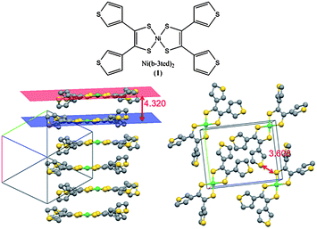 | ||
| Fig. 1 Molecular and packing structure of 1,12 showing a large interplanar distance, and large S–S shortest contacts. Structures redrawn from data available through the CCDC.15 | ||
In order to investigate the films grown by electrooxidation of [1][TBA], a three-electrode cell was set up using either an indium tin oxide (ITO) coated glass electrode, or an interdigitated platinum electrode array (electrode gap 2 μm) as a working electrode. By maintaining a potential sufficient to oxidise the monoanionic TBA salt (0.5 V vs.Ag/AgCl), films of neutral 1 could be deposited on the working electrodes.‡ The films were grown potentiostatically to ensure the complete oxidation to the neutral species upon deposition, but also to ensure that the potential did not become sufficient to effect polymerisation of the pendent thienyl groups during film growth.12 After an initial drop in current, due to the local depletion of the dithiolene salt, a stable current was maintained throughout film growth, beyond total electrode coverage, suggesting the deposition of a conducting film on the working electrode (Fig. 2). The grown films were then washed by immersing in a fresh acetonitrile solution for 1 min before drying in a vacuum desiccator overnight. Sufficient quantities of 1a could be harvested from the electrode for elemental analysis, and the purity compared to chemically synthesised 1 (Table 1). Excellent agreement was observed for both C and N, however the hydrogen content of 1a was rather high. Whilst this could be attributed to impurities present in the film, the excellent agreement of the C and N values with the theoretical levels, suggest that it is rather a result of the small quantity of material provided for analysis, than the presence of residual organic doping.
![Potentiostatic growth of a thin film of 1 from different electrolyte solutions onto interdigitated platinum electrode arrays at [1][TBA] concentrations of 5 and 10 mM; (inset) resistance measurements of deposited films with errors given in the ESI.](/image/article/2011/SC/c0sc00446d/c0sc00446d-f2.gif) | ||
| Fig. 2 Potentiostatic growth of a thin film of 1 from different electrolyte solutions onto interdigitated platinum electrode arrays at [1][TBA] concentrations of 5 and 10 mM; (inset) resistance measurements of deposited films with errors given in the ESI†. | ||
| Theoretical | Electrodeposited (1a) | Pseudo-drop cast (1b) | |
|---|---|---|---|
| C | 42.33 | 42.31 | 42.41 |
| H | 2.13 | 2.85 | 2.18 |
| N | 0 | 0 | 0 |
Since the presence of even small amounts of dopant would affect the electronic properties of a material,11 and because the nature of the dopant will affect the measured conductivity of the doped film, electrodeposition was performed from several background electrolyte solutions (TBABF4, TEABF4 and TEAPF6), at dithiolene concentrations of 5 and 10 mM. Such a test is a very sensitive measure of the extent of residual ion doping in the grown films, and could detect trace ion dopants at a level well below the detection limits of elemental analysis. The resistance of the deposited films was measured by depositing films over a working electrode consisting of an interdigitated array of platinum electrodes (electrode gap 2 μm). The extent of film growth was controlled by fixing the charge passed (5 mC) for each sample so that, by measuring the resistance of the films, the resistivities (and, hence, the conductivities) of the grown films could be directly compared. All conditions were run in duplicate (Test 1 and Test 2) to assess the reproducibility of the deposition process. The resistances of the films from each electrolyte, and at each dithiolene concentration, were broadly similar, varying by just one order of magnitude, suggesting minimal residual doping in the films. However, the resistances of the samples grown at higher dithiolene concentrations (10 mM) showed slightly greater variation between the films formed from different electrolytes, than at lower concentrations (5 mM) (Fig. 2 (inset)), suggesting that the slower growth rate of the dilute solutions resulted in films of higher purity.
For the films grown onto ITO, the morphologies were shown by SEM to be crystalline in nature, with crystallites seeming to grow from point defects over the ITO surface. These crystallites branched and, upon collision, continued to grow in new directions. By stirring the solution during film growth, and therefore removing the diffusion control of the growth rate, the morphology of the films could be modified, showing an increase in the branching of the crystallites. This effect was also observed for films grown from more concentrated dithiolene solutions (10 mM). Films formed from concentrated dithiolene solutions, or with stirring, showed a predominance of a criss-crossed network of crystallites, whilst those formed from dilute solutions without stirring showed a more lamellar arrangement of crystallites (Fig. 3). Due to the more continuous crystalline regions, and the increased purity of the films grown under diffusion control, further studies were performed without stirring on dilute dithiolene solutions (5 mM).
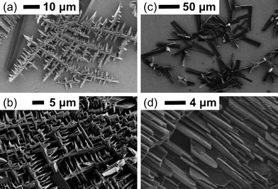 | ||
| Fig. 3 SEM images of electrodeposited films of 1 on ITO: (a) initial crystallite formation in concentrated (10 mM) monomer solution with stirring; (b) film morphology from concentrated (10 mM) monomer solution with stirring; (c) initial crystallite formation in dilute (5 mM) monomer solution without stirring; (d) film morphology from dilute (5 mM) monomer solution without stirring. | ||
Electrodeposited films could be grown over the whole interdigitated electrode region to a similar thickness to those formed by pseudo-drop casting (∼20 μm) by a trial-and-error method. Film thickness was measured after the conductivity and morphology studies were complete by snapping the substrate electrode through the film, and observing the film profile by SEM. The conductivities of the electrodeposited films could therefore be directly compared to the solution processed films, and was shown to be 2 × 10⁻⁹ S cm−1, ∼40 time greater than that of the pseudo-drop cast film (5 × 10⁻¹¹ S cm−1).
Organic semiconductors have been shown to have very different electronic properties, depending on the polymorph that the material crystallises in, reflecting the different intermolecular interactions in the crystal lattice.17–19 It is conceivable that the process of electrodeposition may, in some instances, have an effect on the polymorph that forms on the electrode, since only conducting crystallites will grow. This effect is commonly observed in conventional galvanostatic electrocrystallisation.20Thin-film XRD was carried out on films of 1a and 1b grown onto ITO substrates to investigate the structure of the crystallites present in the film. The results showed that, although some preferred orientation may exist in 1a, shown by the difference in relative peak heights compared to 1b, the unit cell dimensions are essentially the same for both films, thus the crystal structure is the same as that of the only polymorph observed by single crystal XRD (Fig. 4). It should be noted that, although several distinct shapes of single crystal have been isolated by the slow evaporation of DCM (needles and blocks), in all cases the unit cell dimensions are same.
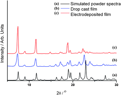 | ||
| Fig. 4 Thin film XRD data for 1a and 1b deposited on an ITO coated glass electrode, compared to a generated powder pattern from single crystal data of 1 using the powder XRD pattern generation software of Mercury 2.3 (CCDC).16 | ||
By comparing the surface morphology of 1a and 1b by SEM, the increased conductivity of the electrodeposited film can be better understood. Both films are of the same thickness, and cover the whole interdigitated region, however, for 1a the crystallites are larger, and have a smaller size distribution (Fig. 5). Crystallites, commonly of widths >10 μm, could easily bridge the 2 μm electrode gap, giving a conductivity measurement closer to the single-crystal value. However, larger crystallites are perhaps not the complete answer, as is shown by the relatively small increase in conductivity of the single crystal over the pressed pellet. What is more likely to result in an increase in the conductivity is the improved electronic contact of the crystallites with the electrode, and with each other. Crystal growth will only propagate if a good electronic contact with the electrode is made, thus the film is dominated by crystallites that have a good electronic connection with the electrode (Fig. S2, ESI†), as those that do not will stop growing. This Darwinian model of film formation in 1a contrasts with the random arrangement of crystallites deposited over the electrodes in 1b. Also, for 1a, crystallites connect at branch points or collisions sites, in both cases providing intimate contact between the crystallites, whereas for 1b, inter-crystalline links are formed by the crystallisation of the small amount of 1 dissolved in the solvent upon drop casting.
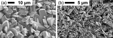 | ||
| Fig. 5 (a) SEM image of a thin film of 1a formed by potentiostatic electrodeposition; (b) SEM image of thin film of 1b formed by pseudo-drop casting. | ||
As continuous films could be deposited over an interdigitated electrode array, the field effect characteristics of a bottom-contact FET device could be investigated. The devices showed only minimal gate dependence, and low mobility values for both the electron and hole channel (μ ∼ 1 × 10⁻⁸ cm2 V−1 S−1) (Fig. S3 ESI†). The poor FET performance of electrodeposited 1 was perhaps not surprising, given the poor intermolecular overlap, as observed in the single crystal, prohibiting efficient transfer of charge in the device. However, it seems that, even for a poor semiconductor, electrodeposition can yield films with a superior morphology for electronic applications, than by solution methods. This is especially apparent for 1, as its solubility in common organic solvents is far too low for effective solution processing, thus in order to form continuous films by solution methods, a pseudo-drop casting method was required, which resulted in a wide range of crystallite sizes, with poor electronic contact with the electrodes, and with each other.
3 Conclusions
Potentiostatic electrodeposition has been shown as a novel technique for the formation of neutral films of [Ni(b-3ted)2], by the electrooxidation of its TBA salt. This technique offers the possibility of forming high-quality polycrystalline films of organic semiconductors that have distinct properties over other deposition methods. The nature of film growth is such that the crystallites form a good electrical contact with the electrode, and with other crystallites, resulting in films with particularly favorable electronic properties. This technique would be appropriate for existing organic semiconductors, that display much higher conductivities, currently deposited by solution or vapour methods. However, it is particularly suited to the systems that are unprocessable by conventional techniques, due to their high boiling point, or poor solubility, and may lead to the formation of high quality films that would otherwise be unobtainable by conventional methods.1 shows poor conductivity as a single crystal, due to the poor overlap of the molecules in the solid state and, as such, is of little practical use for electronic application. However, it serves to demonstrate that, if film growth can propagate, even for a poor molecular conductor, and result in high quality polycrystalline films, then such a technique would be suitable for a large range of systems, with a large range of conductive properties. The technique was demonstrated for a nickel dithiolene, due to its multiple air-stable oxidation states, allowing for a more simple experimental design, and the technique could also be extended to other ditholenes, which have shown much better electronic properties, and a large gate dependence in FET devices.21–25 However, the scope of this technique is not limited to dithiolenes, and would be applicable to systems such as the highly studied polycyclic aromatics.26 For example, pentacene has shown some of the highest reported mobilities (μ > 5 cm2 V−1s−1) as thin films,27 however, due to its insolubility in all common organic solvents, films must be fabricated by more expensive vapour methods, that are unsuitable for large-scale fabrication. Pentacene can form a sodium salt in THF,28 whereupon it readily dissolves, and therefore may be suitable for electrodeposition. This technique has an additional advantage insofar as, for film growth to propagate, the film itself must be conductive thus, for systems with more than one crystalline phase, it is conceivable that the more conducting phase may be deposited by such a process. Future work should focus on expanding this technique to look at the deposition of other organic molecular semiconductors.
Acknowledgements
The authors would like to thank the EPSRC and the Japanese Science and Technology Agency (JST) for financial support.Notes and references
- C. R. Kagan, D. B. Mitzi and C. D. Dimitrakopoulos, Science, 1999, 286, 945–947 CrossRef CAS.
- H. Isotalo, J. Paloheimo, Y. F. Miura, R. Azumi, M. Matsumoto and T. Nakamura, Phys. Rev. B: Condens. Matter, 1995, 51, 1809–1816 CrossRef CAS.
- T. Takahashi, K.-I. Sakai, T. Yumoto, T. Akutagawa, T. Hasegawa and T. Nakamura, Thin Solid Films, 2001, 393, 7–11 CrossRef CAS.
- M. Mas-Torrent and C. Rovira, J. Mater. Chem., 2006, 16, 433–436 RSC.
- B. Noda, M. Katsuhara, I. Aoyagi, T. Mori, T. Taguchi, T. Kambayashi, K. Ishikawa and H. Takezoe, Chem. Lett., 2005, 34, 392–393 CrossRef CAS.
- R. Kato, Chem. Rev., 2004, 104, 5319–5346 CrossRef CAS.
- K. L. Marshall, B. Schudel and I. A. Lippa, LLE Rev., 2006, 106, 112–128 Search PubMed.
- W. E. Buschmann, S. C. Paulson, C. M. Wynn, M. A. Girtu, A. J. Epstein, H. S. White and J. S. Miller, Chem. Mater., 1998, 10, 1386–1395 CrossRef CAS.
- D. de Caro, M. Basso-Bert, H. Casellas, M. Elgaddari, J. P. Savy, J. F. Lamére, A. Bachelier, C. Faulmann, I. Malfant, M. Étienne and L. Valade, C. R. Chim., 2005, 8, 1156–1173 CrossRef CAS.
- G. Cui, W. Xu, C. Guo, X. Xiao, H. Xu, D. Zhang, L. Jiang and D. Zhu, J. Phys. Chem. B, 2004, 108, 13638–13542 CrossRef CAS.
- J. R. Bates, R. W. Miles and P. Kathirgamanathan, Synth. Met., 1996, 76, 313–315 CrossRef CAS.
- T. Anjos, S. Roberts-Bleming, A. Charlton, N. Robertson, A. R. Mount, S. J. Coles, M. B. Hursthouse, M. Kalaji and P. J. Murphy, J. Mater. Chem., 2008, 18, 475–483 RSC.
- M. M. Matsushita, H. Kawakami, E. Okabe, H. Kouka, Y. Kawada and T. Sugawara, Polyhedron, 2005, 24, 2870–2875 CrossRef CAS.
- S. Dalgleish and N. Robertson, Coord. Chem. Rev., 2010, 254, 1549–1558 CrossRef CAS.
- F. H. Allen, Acta Crystallogr., Sect. B: Struct. Sci., 2002, 58, 380–388 CrossRef.
- C. F. Macrae, P. R. Edgington, P. McCabe, E. Pidcock, G. P. Shields, R. Taylor, M. Towler and J. van de Streek, J. Appl. Crystallogr., 2006, 39, 453–457 CrossRef CAS.
- J. Fraxedas, J. Phys.: Condens. Matter, 2008, 20, 180301 CrossRef.
- J. Cornil, J. P. Calbert and J. L. Brédas, J. Am. Chem. Soc., 2001, 123, 1250–1251 CrossRef CAS.
- S. Schiefer, M. Huth, A. Dobrinevski and B. Nickel, J. Am. Chem. Soc., 2007, 129, 10316–10317 CrossRef CAS.
- M. R. Bryce, Chem. Soc. Rev., 1991, 20, 355–390 RSC.
- T. D. Anthopoulos, S. Setayesh, E. Smits, M. Cölle, E. Cantatore, B. de Boer, P. W. M. Blom and D. M. de Leeuw, Adv. Mater., 2006, 18, 1900–1904 CrossRef CAS.
- E. C. P. Smits, T. D. Anthopoulos, S. Setayesh, E. van Veenendaal, R. Coehoorn, P. W. M. Blom, B. de Boer and D. M. de Leeuw, Phys. Rev. B: Condens. Matter Mater. Phys., 2006, 73, 205316 CrossRef.
- T. D. Anthopoulos, G. C. Anyfantis, G. C. Papavassiliou and D. M. de Leeuw, Appl. Phys. Lett., 2007, 90, 122105 CrossRef.
- H. Wada, T. Taguchi, B. Noda, T. Kambayashi, T. Mori, K. Ishikawa and H. Takezoe, Org. Electron., 2007, 8, 759–766 CrossRef CAS.
- J. Y. Cho, B. Domercq, S. C. Jones, J. Yu, X. Zhang, Z. An, M. Bishop, S. Barlow, S. R. Marder and B. Kippelen, J. Mater. Chem., 2007, 17, 2642–2647 RSC.
- M. Bendikov, F. Wudl and D. F. Perepichka, Chem. Rev., 2004, 104, 4891–4945 CrossRef CAS.
- T. W. Kelley, P. F. Baude, C. Gerlach, D. E. Ender, D. Muyres, M. A. Haase, D. E. Vogel and S. D. Theiss, Chem. Mater., 2004, 16, 4413–4422 CrossRef CAS.
- K. H. J. Buschow, J. Dieleman and G. J. Hoijtink, J. Chem. Phys., 1965, 42, 1993–1999 CAS.
Footnotes |
| † Electronic supplementary information (ESI) available: Full details of conditions given for all experimental techniques used in this study. Fig. S1: SEM images of films of 1 on ITO formed by; (a) drop coating; (b) spin coating; (c) pseudo-drop coating. Fig. S2: SEM image of initial crystallite growth by electrodeposition over an interdigitated electrode array. Fig: S3: FET characteristics of 1a. Table S1: Resistance measurements of deposited films of 1a with errors given. See DOI: 10.1039/c0sc00446d |
| ‡ Electrodeposition was performed at room temperature on a ∼5 or ∼10 mM [1][TBA] solution in dry MeCN, using 0.1 M TBABF4, TEABF4 or TEAPF6, as supporting electrolyte in a three-electrode cell. The working electrode was either an indium tin oxide (ITO) coated glass electrode or an FET substrate. The FET architecture comprised an n-doped silicon wafer as gate electrode, with a 300 nm thermally grown SiO2 (with a capacitance (Ci) of 17 nF cm−2) layer as dielectric. The platinum source and drain electrodes were arranged as an interdigitated electrode array deposited by photolithography (for which the channel dimensions correspond to W = 100 cm width and L = 2 μm length). During the electrodeposition, the gate contact was masked with chemically resistant Capton tape. The reference electrode was Ag/AgCl (0.1 M KCl), calibrated for ferrocene–ferrocenium (+0.55 V), and the counter-electrode was a Pt gauze. |
| This journal is © The Royal Society of Chemistry 2011 |