Fluorescent bracelet-like Cu@cross-linked poly(vinyl alcohol) (PVA) microrings by a hydrothermal process†
Feng-Jia
Fan
,
Yong-Jie
Zhan
,
Jian-Hua
Zhu
,
Ji-Ming
Song
and
Shu-Hong
Yu
*
Division of Nanomaterials and Chemistry, Hefei National Laboratory for Physical Sciences at Microscale, Department of Chemistry, University of Science and Technology of China, Hefei 230026, P. R. China. E-mail: shyu@ustc.edu.cn; Fax: 0086 551 3603040
First published on 26th July 2011
Abstract
Novel bracelet-like Cu@cross-linked poly(vinyl alcohol) (PVA) microrings have been prepared through a PVA-assisted hydrothermal process. Bracelet-like microrings are composed of inner copper nanorings and outer cross-linked PVA beads. The formation of bracelet-like microrings consists of two steps, i.e. the growth and self-coiling of PVA-wrapped copper nanowires and corresponding adhering of cross-linked PVA to form bracelet-like structures. Copper nanowires are formed by reduction from a mixed copper source consisting of CuCl2 and CuBr in the presence of NaBr by PVA. When an appropriate amount of NaBr was added, a product with a high yield of microrings can be obtained. A further investigation on ultra-thin section TEM images indicates that addition of the appropriate amount of NaBr leads to thinner copper nanowires within the crosss-linked PVA coatings. We proposed that thinner copper nanowires have less elastic resistance during bending processes, so PVA wrapped copper nanowires are more easily bent arbitrarily during vigorous Brownian motion at 210 °C. When two ends of one single nanowire join, the formation of van der Waals bonds and diminishing of the interfacial area through overlapping compensate the elastic resistance to get stable ring-like structures.
Introduction
Nanoring and nanospring structures have drawn much attention during the last few years due to their shape dependent novel magnetic, electron transport, enhanced localized electromagnetic properties and their potential applications in energy storage and release at nanoscale.1–3 Up to now, various methods have been developed to fabricate nanoring structures. Au,4Ag5 and TiO26 nanorings have been synthesized respectively by using silver nanoplates, folded DNA molecules and macroporous polymers as templates. Magnetic dipoles have been utilized to synthesize flux-closure nanorings, such as Co7 and Ni–Co alloy nanorings.8 CdS nanorings9 have been prepared based on morphology control of nanocrystals that hold intrinsic hexagonal symmetry. Most nanorings fabricated by the above methods are either polycrystalline or assembled from individual nanoparticles. Nanoring structures formed through self-coiling of nanowires or nanobelts are interesting as they have more complex formation mechanisms.ZnO nanorings10 have been prepared through a vapor–solid process and a spontaneous polarized surface induced self-coiling mechanism has been applied to interpret the formation process. In the solution phase, Ag2VO4,11CuO,12VO213 and Na2Ti6O1314 nanorings can also be prepared by hydrothermal approaches with the help of electrostatic interactions between polarized surfaces. For carbon nanotubes, there are many studies based on spontaneous coiling of carbon nanotubes to form nanoring structures,15–19 and several models have been built to capture the competition of bending force and self attraction of carbon nanotubes. Formation of self-coiled nanorings always accompanies the reduction in the potential energy of nanobelts or nanowires by minimizing elastic forces, forming chemical bonds, creating van der Waals bonds and vanishing interface areas under certain circumstance, but have to overcome the elastic resistance of nanowires. The complex formation processes give insights into the electrostatic force, van der Waals force and interface tensions at nanoscale and novel shape dependent properties could be found.
Up to now, there are several reports on self-coiling of metal nanowires to form nanoring structures. Silver nanorings were discovered in a reductive reaction solution by using the polyol method.20,21Au nanosprings were prepared through the polymer shell induced coiling of Au nanowires.22 However, to the best of our knowledge, there is no report on the formation of nanoring structures through self-coiling of copper nanowires, although copper is a metal with good flexibility like silver and gold.
In this article, we demonstrate the formation of bracelet-like Cu@cross-linked poly(vinyl alcohol) PVA microrings which are composed of inner copper nanorings and outer cross-linked PVA beads through a PVA-assisted hydrothermal process. The formation process of Cu@cross-linked PVA microrings includes two steps: self coiling of PVA wrapped copper nanowires reduced from a mixed copper source and adhering of cross-linked PVA aggregates to form microbeads. An appropriate concentration of Cu+ was controlled through adding a certain amount of NaBr, as a lower concentration of Cu+ yields thinner copper nanowires which makes them more easily bent in PVA solution at a high temperature of 210 °C. Further increasing the amount of NaBr makes Cu+ difficult to reduce. Formation of van der Waals interactions and diminishing the interface area compensate the elastic resistance of copper nanowires and copper nanorings were stabilized by adhered cross-linked PVA to form novel Cu@cross-linked bracelet-like microring structures.
Experimental
Materials
All the reagents (analytical-grade purity) were purchased from Shanghai Chemical Reagents Co. and used without any further purification.Synthesis procedure of Cu@cross-linked PVA microrings
In a typical hydrothermal process, 0.058 g CuBr, 0.028 g CuCl2, and 0.02 g NaBr were added into a Teflon-lined stainless steel autoclave with a capacity of 50 ml, then the autoclave was filled with 40 ml PVA solution (1.5 wt%, pH 9.5, modulated by NaOH solution). After stirring the solution for 5 min, the autoclave was sealed, heated in an oven at 210 °C for 48 h, and then naturally cooled to room temperature, and a brownish red floccule formed, which was then collected, washed with diluted ammonia twice to remove excess CuBr, then washed with distilled water and ethanol several times to remove ions and possible remnants, and vacuum-dried for further characterization.Characterization
The final products were characterized by various techniques. X-Ray powder diffraction (XRD) was carried out on a Rigaku D/max-rA X-ray diffractometer with Cu-Kα radiation (λ = 1.54178 Å). A scan rate of 0.05° s−1 was applied to record the pattern in the 2θ range of 10–90°. The morphologies of the samples were further characterized using a field emission scanning electron microscope (FESEM, JEOL JSM-6700F, operated at 5 kV), and an Olympus optical microscope with a digital CCD camera. Fluorescent image was recorded under a Zeiss Axiovert 200 fluorescence microscope and Axiocam-HS digital camera. High resolution TEM images (HRTEM) and the corresponding selected-area electron diffraction (SAED) patterns were recorded on a JEOL-2010 high-resolution transmission electron microscope at an acceleration voltage of 200 kV. Room temperature IR and PL spectra were measured on a Bruker Vector-22 FT-IR spectrometer and Hitachi F7000 PL spectrometer respectively.Results and discussion
A mixture of CuCl2 and CuBr was reduced by PVA solution in the presence of an appropriate amount of NaBr at a temperature of 210 °C for 48 h. When the reaction was completed, there was a large amount of un-reacted CuBr coexisting with the Cu@cross-linked PVA nanocomposite (Fig. 1b), but un-reacted CuBr can be easily washed out with diluted ammonia, also we can remove CuBr from the Cu@cross-linked PVA nanocomposite by utilizing the difference in densities, as CuBr with much larger density than water will deposit while the Cu@cross-linked PVA nanocomposite will float or be suspended in water. The X-ray diffraction pattern of purified sample can be indexed to the fcc Cu phase in agreement with literature data (JCPDS 4-836). The FTIR spectrum of sample (ESI, Fig. S1†) show similar features to those reported previously that there are some –OH bonds remaining and some C![[double bond, length as m-dash]](https://www.rsc.org/images/entities/char_e001.gif) O bonds formed due to the cross-linking reaction.23X-Ray photoelectron spectrum can provide the surface composition information of a material. With the help of XPS, we can conform that Cu nanowires are well wrapped within the cross-linked PVA, as the copper signal in XPS is hardly detectable while the carbon signal is very strong (ESI, Fig. S2†).
O bonds formed due to the cross-linking reaction.23X-Ray photoelectron spectrum can provide the surface composition information of a material. With the help of XPS, we can conform that Cu nanowires are well wrapped within the cross-linked PVA, as the copper signal in XPS is hardly detectable while the carbon signal is very strong (ESI, Fig. S2†).
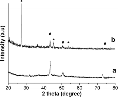 | ||
| Fig. 1 XRD pattern of purified product (a) and product with CuBr retained (b). # Cu phase, * CuBr phase. | ||
The morphologies of bracelet-like microrings were characterized by FESEM and photo-microscopy to facilitate the observation. A general overview FESEM image in Fig. 2a shows that the product is mainly composed of Cu@cross-linked PVA microrings with diameters in the range from 20 to 70 μm and there are some coexisting microcables. The SEM image in Fig. 2b shows a single bracelet-like microring composed of several tens of cross-linked PVA beads, and some beads coalesced during the growth process. The diameters of the beads range from 2 to 4 μm. A Cu nanowire within transparent cross-linked PVA beads is demonstrated in a typical optical image (Fig. 2c). Due to the large diameters of microrings and the fluctuating diameters of cross-linked PVA beads, only part of the Cu nanowire in the focal plane is clearly visible. The two ends of the Cu nanowire joined with some mismatch. The fluorescent microscopy image of two neighboring microrings in Fig. 2d indicates that the bracelet-like microrings display strong green emission (ESI, Fig. S3†), which is consistent with what was found for the necklace-like microcables.24
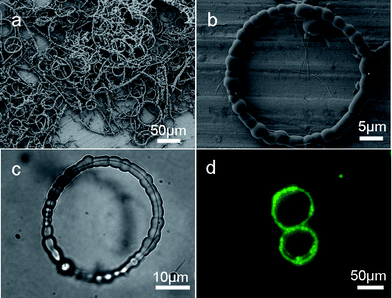 | ||
| Fig. 2 (a) SEM image of the bracelet-like microrings. (b) SEM image of a single microring composed of several tens of cross-linked PVA beads. (c) Optical image of a single microring indicates the thin nanowire within the cross-linked PVA coating. (d) Fluorescent microscopy image of two adjacent microrings. | ||
TEM and HRTEM observation on the ultra-thin section of the samples was performed to further investigate the inner Cu nanowires within the cross-linked PVA coating. It is interesting to find that besides a single nanowire, there are also two or three Cu nanowire sections within cross-linked PVA coatings (Fig. 3). Two parallel aligned inner copper nanowires in Cu@cross-linked PVA nanocables and raft-like bundle structures of Ag@cross-linked PVA nanocables have been discovered in our previous reports.23,25 The possible formation mechanism of dual and triple Cu nanowire sections within cross-linked PVA will be discussed below.
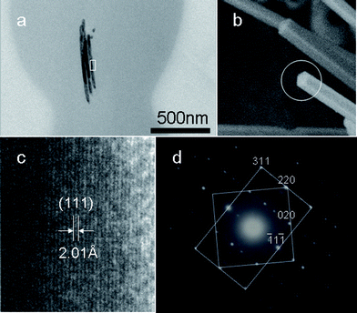 | ||
| Fig. 3 (a) TEM image of an ultra-thin section of the sample. (b) SEM image of Cu nanocables wrapped with little cross-linked PVA obtained after reaction for 3 h. (c) HRTEM image taken on the area marked in (a), and (d) SAED pattern indicating that five-fold twinning exists in the inner Cu nanowires. | ||
As the HRTEM image in Fig. 3c taken from marked area in Fig. 3a shows, the lattice fringes with a measured d spacing of 2.01 Å would correspond to the (111) lattice planes. The corresponding SAED pattern is consistent with that previously reported for the penta-twinned Cu and Au26,27nanorods. The superposition of square [001] and rectangular [1![[1 with combining macron]](https://www.rsc.org/images/entities/char_0031_0304.gif) 2] zone patterns of the fcc structure indicates the formation of the five-fold twinning. The SEM image in Fig. 3b taken on Cu nanowires wrapped with little PVA was obtained after reaction for 3 h. The result is different from those obtained previously for Cu@cross-linked PVA nanocables with single crystalline Cu nanowires within nanocables.23 The nanowires within cross-linked PVA grow preferentially along the [110] direction, which is in agreement with the results reported for Cu and Au26,27nanorods, as well as Cu@cross-linked PVA nanocables.23
2] zone patterns of the fcc structure indicates the formation of the five-fold twinning. The SEM image in Fig. 3b taken on Cu nanowires wrapped with little PVA was obtained after reaction for 3 h. The result is different from those obtained previously for Cu@cross-linked PVA nanocables with single crystalline Cu nanowires within nanocables.23 The nanowires within cross-linked PVA grow preferentially along the [110] direction, which is in agreement with the results reported for Cu and Au26,27nanorods, as well as Cu@cross-linked PVA nanocables.23
The key parameter for the formation of the ring structure was discussed. In our previous report on the synthesis of Cu@cross-linked PVA nanocables, we found that the reducing reactions of the CuCl2 precursor to Cu nanowires included two distinct steps: from CuCl2 to CuCl and then to Cu.23 We also prepared necklace-like Cu@cross-linked PVA microcables by using CuCl as a co-precursor.25 In the present experiment, we find if CuBr with a lower value of solubility constant is chosen as a co-precursor and an appropriate amount of NaBr is added, many Cu@cross-linked PVA microrings are formed after hydrothermal reaction.
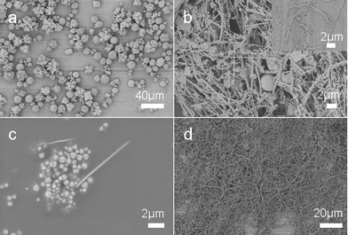
The SEM image in Fig. 4a shows that the product is mainly composed of necklace-like microcables and only a small fraction of the product coils into microring structures when CuBr is used as the only co-precursor. The yield of microrings can increase from about 5% to about 50% by adding a certain amount of NaBr (0.02 g) as shown in Fig. 4b. A further increase in the amount of NaBr added does not lead to a higher yield of microrings. When 0.04 g NaBr is added into the reaction system, less cross-linked PVA can be obtained and the product is mainly composed of irregular cross-linked PVA (Fig. 4c). This trend is more obvious with adding 0.06 g NaBr (Fig. 4d).
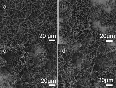 | ||
| Fig. 4 SEM images of the samples obtained through keeping CuCl2 and CuBr constant and varying the amount of NaBr from 0 g (a), 0.02 g (b), 0.04 g (c) to 0.06 g (d). | ||
To illuminate the influence of NaBr on the growth process of Cu nanowires, ultra-thin section TEM was applied to obtain detailed information on nanowires within the cross-linked PVA coating. TEM images in Fig. 5 taken on the ultra-thin crossed section of the sample show that the diameters of inner Cu nanowires ranging from 30 to 90 nm prepared by adding 0.02 g NaBr are thinner than that of the obtained sample without adding any NaBr, of which the diameters range from 90 to 100 nm (Figs. 5 and 6). As we mentioned above, copper nanowires form by reducing reaction from Cu+. According to the solubility equilibrium eqn (1), the NaBr added here can reduce the concentration of Cu+ according to eqn (2), so we can conclude that a lower concentration of Cu+ in the reaction solution yields Cu nanowires with thinner diameters, but Cu+ is difficult to reduce by PVA if more than 0.04 g NaBr is added. We also tried to add NaI into the reaction solution, but no cross-linked PVA could be obtained, as CuI has a much lower solubility constant than CuBr.
 | (1) |
 | (2) |
 | ||
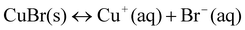
| Fig. 5 Ultra-thin section TEM images of product mainly composed of microrings. The product was obtained after reaction for 48 h at 210 °C, the Cu sources (0.028 g CuCl2 and 0.058 g CuBr) were reduced by PVA solution (1.5 wt%, pH 9.5) in the presence of 0.02 g NaBr. White arrows in TEM images indicate the cross-sections of copper nanowires and black arrows point to the cross-sections of cross-linked PVA coating. | ||
 | ||
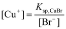
| Fig. 6 Ultra-thin section TEM images of the product mainly composed of necklace-like microcables. The product was obtained after reaction for 48h at 210 °C, the Cu sources (0.028 g CuCl2 and 0.058 g CuBr) were reduced by PVA solution (1.5 wt%, pH 9.5) in the absence of NaBr. White arrows in TEM images pointed to the cross-sections of copper nanowires and black arrows pointed to the cross-sections of cross-linked PVA coating. | ||
Time dependent experiments were performed to investigate the shape evolution process (Fig. 7). The SEM images show products obtained after reaction for different times. When the reaction is prolonged for two hours, the product is CuBr microspheres which are confirmed by PXRD analysis (ESI, Fig. S4†) and there are almost no cross-linked PVA or copper nanowires formed. Copper nanowires protected by PVA appeared after reaction for 3 h, and nanospirals formed through a self-coiling process of Cu nanowires could be observed. As the reaction time was prolonged, soft and sticky aggregates of cross-linked PVA appeared. When the reaction time reached 6 h, bracelet-like microrings appeared and the morphology of the product did not change much after that.
 | ||
| Fig. 7 SEM images of product obtained after reaction for different times: (a) 2 h, (b) 3 h, (c) 4 h, and (d) 6 h. The product was prepared at 210 °C. | ||
Up to now, two typical nanoring structures have been widely investigated, crystalline plane polarized semiconductors and carbon nanotube nanorings. Several crystalline plane polarized semiconductor nanorings, such as SnO228 and ZnO nanorings,10 have been prepared through the solid–vapor process, the formation mechanism of which was attributed to the minimization of electrostatic energy between polarized crystal planes. In the hydrothermal process, Ag2VO4,11CuO,12VO213 and Na2Ti6O1314 nanorings can also be obtained with the help of electrostatic interaction of polarized crystal planes. Apparently, the polarized surface induced bending mechanism can not be applied to interpret the self-coiling process of Cu nanowires, because there is no polarized crystal plane in Cu.
Formation of nanorings coiled from carbon nanotubes, which has been widely studied,15–19 shows some similarities with the formation of Cu@cross-linked PVA microrings. The coiling of carbon nanotubes can be activated by different kinds of energy, such as ultrasonic15,18 and microwave19 irradiation, and the coiled configurations are stabilized by van der Waal binding, chemical bonding and interfacial tension. In our experiment, vigorous Brownian motion of PVA-wrapped copper nanowires under thermal activation makes them bend and remove in PVA solution arbitrarily, and we propose that the van der Waals force between PVA molecules wrapped around copper nanowires and the interfacial tension between PVA wrapped around copper nanowires and PVA solution are two major forces to stabilize coiled copper nanorings and parallel aligned nanowires before being thickly wrapped by cross-linked PVA,
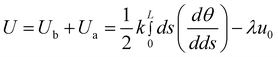
Herein, we use the simplest model which has been applied to study the bending process of carbon nanotubes19 to qualitatively describe the competition of bending and self-attraction of copper nanowires before being thickly coated by PVA. As eqn (3) shows, the total energy U of copper nanowires is composed of a bending energy Ub and a self-attractive energy Ua.19k is the bending stiffness of copper nanowires, u0 is the energy per unit length of overlapping which is induced by the formation of van der Waals bonding and the vanishing of interface area, L is the length of nanowires, s is the arc length along the nanowire contour, θ is the angular position, r is the ring radius and λ is the overlapping length.19
 | (3) |
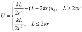
For nanorings, S = θr and λ = L − 2πr. L > 2πr is necessary to form coiled structures, and a longer overlapping length leads to more stable nanorings.
 | (4) |
Before the two ends of nanowires connect with each other, certain activation energy is needed to overcome the energy peak of Umax = 2π2k/L for L = 2πr during the bending process. Thermal activation was reasonably proposed to be the activation energy in the case of carbon nanotube ring synthesis.19 As we know, copper is a metal with very good ductility especially at elevated temperature. In our experiment, CuBr combined with NaBr were applied to prepare Cu nanowires with thinner diameters which decreased the bending stiffness k. A relatively high temperature of 210 °C also can provide the thermal activation to overpass the energy peak, as Brownian motion of PVA wrapped copper nanowires in PVA solution is vigorous at such high temperature.
Based on the observation of shape evolution and the above analysis, a possible formation mechanism is proposed. As Scheme 1 shows, the Cu nanowires wrapped with PVA formed at the initiate stage. Due to the high reaction temperature of 210 °C, PVA-wrapped copper nanowires undergo vigorous Brownian motion in PVA solution. They are bent and removed arbitrarily, when two nanowires contact with each other, van der Waals force and interface tensions can stabilize them to form parallel-aligned bundle structures. If the two ends of one single nanowire join, two ends tend to get more overlap length to form van der Waals bonding and diminish the interfacial area to decrease the potential energy. Succeeding cross-linked PVA will aggregate and be absorbed onto PVA wrapped copper nanowires to form bracelet-like microrings. The cross-linked PVA also acts as a good binder to stabilize the ring structures of Cu nanowires so the yield of microrings is relatively high.
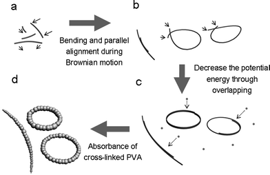 | ||
| Scheme 1 Illustration of the formation mechanism of Cu@PVA microrings. (a) PVA-wrapped Cu nanowires form at the initial stage, they are bent and removed during Brownian motion arbitrarily. (b) Formation of two parallel-aligned nanowires and joining of two ends of one single nanowire under thermal activation. (c) PVA wrapped copper nanowires tend to overlap to decrease the potential energy. (d) Absorption of cross-linked PVA to form bracelet-like microrings. | ||
Conclusions
In summary, unique fluorescent bracelet-like Cu@ cross-linked PVA microrings can be synthesized by a simple one-pot hydrothermal process. The CuBr and an appropriate amount of NaBr played critical roles in the synthesis of bracelet-like microrings. The vigorous Brownian motion of PVA wrapped copper nanowires in PVA solution makes PVA-wrapped copper nanowires bend and move. When the two ends of one single nanowires join, they tend to overlap with the help of van der Waals force and interfacial tension, they are also two major forces to stabilize copper nanorings before being coated with thick cross-linked PVA. The succeeding aggregation of cross-linked PVA can stabilize the ring-like structures to form bracelet-like microrings. The present study provides a first study on nanoring formation coiled from copper nanowires.Acknowledgements
S. H. Yu acknowledges the funding support from the National Basic Research Program of China (2010CB934700), the National Natural Science Foundation of China (NSFC, Nos. 91022032, 50732006), and International Science & Technology Cooperation Program of China (2010DFA41170).References
- S. L. Tripp, R. E. Dunin-Borkowski and A. Wei, Angew. Chem., Int. Ed., 2003, 42, 5591–5593 CrossRef CAS.
- E. M. Larsson, J. Alegret, M. Kall and D. S. Sutherland, Nano Lett., 2007, 7, 1256–1263 CrossRef CAS.
- J. Xu, H. Wang, C. C. Liu, Y. M. Yang, T. Chen, Y. W. Wang, F. Wang, X. G. Liu, B. G. Xing and H. Y. Chen, J. Am. Chem. Soc., 2010, 132, 11920–11922 CrossRef CAS.
- L. P. Jiang, S. Xu, J. M. Zhu, J. R. Zhang, J. J. Zhu and H. Y. Chen, Inorg. Chem., 2004, 43, 5877–5883 CrossRef CAS.
- A. A. Zinchenko, K. Yoshikawa and D. Baigl, Adv. Mater., 2005, 17, 2820–2823 CrossRef CAS.
- D. K. Yi and D. Y. Kim, Nano Lett., 2003, 3, 207–211 CrossRef CAS.
- H. Zhang, C. X. Zhai, J. B. Wu, X. Y. Ma and D. R. Yang, Chem. Commun., 2008, 5648–5650 RSC.
- M. J. Hu, Y. Lu, S. Zhang, S. R. Guo, B. Lin, M. Zhang and S. H. Yu, J. Am. Chem. Soc., 2008, 130, 11606–11607 CrossRef CAS.
- B. Liu and H. C. Zeng, J. Am. Chem. Soc., 2005, 127, 18262–18268 CrossRef CAS.
- X. Y. Kong, Y. Ding, R. Yang and Z. L. Wang, Science, 2004, 303, 1348–1351 CrossRef CAS.
- G. Z. Shen and D. Chen, J. Am. Chem. Soc., 2006, 128, 11762–11763 CrossRef CAS.
- X. Q. Wang, G. C. Xi, S. L. Xiong, Y. K. Liu, B. J. Xi, W. Yu and Y. Qian, Cryst. Growth Des., 2007, 7, 930–934 CAS.
- M. Li, F. Y. Kong, Y. X. Zhang and G. H. Li, CrystEngComm, 2011, 13, 2204–2207 RSC.
- C. Y. Xu, J. Wu, L. X. Lv, J. X. Cui, Z. Q. Wang, Y. D. Huang and L. Zhen, CrystEngComm, 2011, 13, 2674–2677 RSC.
- R. Martel, H. R. Shea and P. Avouris, Nature, 1999, 398, 299 CrossRef CAS.
- S. Zhang, S. Zhao, M. Xia, E. Zhang and T. Xu, Phys. Rev. B: Condens. Matter, 2003, 68, 245419 CrossRef.
- X.-H. Zhong, Y.-L. Li, F. Hou and J.-M. Feng, Appl. Phys. A: Mater. Sci. Process., 2008, 92, 709–713 CrossRef CAS.
- J. Geng, Y. K. Ko, S. C. Youn, Y. H. Kim, S. A. Kim, D. H. Jung and H. T. Jung, J. Phys. Chem. C, 2008, 112, 12264–12271 CAS.
- J. G. Duque, J. A. Eukel, M. Pasquali and H. K. Schmidt, J. Phys. Chem. C, 2009, 113, 18863–18869 CAS.
- H. M. Gong, L. Zhou, X. R. Su, S. Xioo, S. D. Liu and Q. Q. Wang, Adv. Funct. Mater., 2009, 19, 298–303 CrossRef CAS.
- L. Zhou, X. F. Fu, L. Yu, X. Zhang, X. F. Yu and Z. H. Hao, Appl. Phys. Lett., 2009, 94, 153102 CrossRef.
- J. Xu, H. Wang, C. Liu, Y. Yang, T. Chen, Y. Wang, F. Wang, X. Liu, B. Xing and H. Chen, J. Am. Chem. Soc., 2010, 132, 11920–11922 CrossRef CAS.
- J. Y. Gong, L. B. Luo, S. H. Yu, H. S. Qian and L. F. Fei, J. Mater. Chem., 2006, 16, 101–105 RSC.
- S. Zhang, H. Y. Zhu, Z. B. Hu, L. Liu, S. F. Chen and S. H. Yu, Chem. Commun., 2009, 2326–2328 RSC.
- Y. J. Zhan and S. H. Yu, J. Am. Chem. Soc., 2008, 130, 5650–5651 CrossRef CAS.
- I. Lisiecki, A. Filankembo, H. Sack-Kongehl, K. Weiss, M. P. Pileni and J. Urban, Phys. Rev. B: Condens. Matter, 2000, 61, 4968–4974 CrossRef CAS.
- C. J. Johnson, E. Dujardin, S. A. Davis, C. J. Murphy and S. Mann, J. Mater. Chem., 2002, 12, 1765–1770 RSC.
- R. S. Yang and Z. L. Wang, J. Am. Chem. Soc., 2006, 128, 1466–1467 CrossRef CAS.
Footnote |
| † Electronic Supplementary Information (ESI) available. See DOI: 10.1039/c1ra00227a/ |
| This journal is © The Royal Society of Chemistry 2011 |