Synthesis of a tunable MgB2/Nano-Graphene/MgB2–Josephson junction-like structure for electronic devices
Khaled M.
Elsabawy
*ab
aMaterials Science Unit, Chemistry Department, Faculty of Science, Tanta University, Tanta, 31725, Egypt
bMaterials Science Unit, Chemistry Department, Faculty of Science, Taif University, Alhawyah, 888, Saudi Arabia. E-mail: ksabawy@yahoo.com
First published on 30th September 2011
Abstract
The present investigations show a new trend, introducing the possibility of forming superconductor/conductor/superconductor Josephson junction-like structure using MgB2 as a model for the superconducting species and layered graphene for the conducting species. The MgB2/Graphene/MgB2 junction was synthesized in three steps, firstly MgB2 was synthesized by a conventional solid state reaction in a nitrogenated sealed tantalum ampoule. Secondly, a chemical vapor deposition (ICVD) technique was applied to deposit a few layers of graphene on the surfaces of two identical smoothly polished pellets of MgB2 with the same diameter and thickness. Thirdly, the two pellets with deposited graphene layers were formulated into one pellet using a hydrostatic compressor at 4 Ton cm−2. The structural and nano-structural features of the resulting interference junction were investigated by Raman spectra, XRD, AFM/STM and SE-microscopy with EDX-analysis. It was concluded that the manufactured MgB2/Graphene/MgB2 junction was controlled by many parameters.
I. Introduction
Graphene, a two-dimensional (2D) sheet of sp2-hybridized carbon arranged in a honeycomb lattice, has received much attention in the past few years due to its exceptional electronic and optical properties1–3 Its naturally thin plane geometry, unusual band structure and high carrier mobility make it an ideal material for applications in future optoelectronic devices.4–6 However, the applications of graphene have been hindered by its poor processability which is mainly caused by the high inter-layer attraction energies. Similar to carbon nanotubes (CNTs), the problem can be overcome by functionalization on the sheet surface by either a covalent or a non covalent method.7 After reacting with strong oxidants, graphene oxide (GO) with hydroxyl, epoxyl and carboxyl groups on the sheet surface can be obtained.8–10 A number of types of covalently functionalized GO have been prepared by utilizing the above functional groups.11,12 Such modified GO can be also used as an electron-accepting material in organic solar cells due to its unique structure and excellent electronic properties.13Many investigators have introduced efficient and reliable synthesis protocols for high-quality graphene layers. To date, several techniques have been established: (i) precipitation from silicon carbide,14 (ii) mechanical exfoliation from graphite,15,16 (iii) reduction of exfoliated graphite oxide,17,18 (iv) thermal expansion of graphite oxide,19 (v) laser desorption20 and (vi) growth by chemical vapor deposition (CVD) on metal surfaces.21,24 The latter is especially interesting for ferromagnetic materials and it was demonstrated that the spin polarization of a Ni(III) substrate can be cloned almost completely into a graphene over-layer.25 This allows the design of sources of spin polarized electrons that are fully prevented from ageing when exposed to reactive gases. Despite these promising perspectives, little is known about the actual growth mechanism of graphene on metal surfaces.26
Few articles were found in literature concerning superconducting quantum interference devices such as27,28 Ginit et al.28 who reported the possibility of forming Al/Graphene/Pd junction as electronic superconducting quantum interference devices.
The major goal of the present article is to introduce a novel simple technique to manufacture a MgB2/Graphene/MgB2 junction as an electronic graphene superconducting quantum interference device, a powerful future platform for nanoscale magnetometry and fundamental transport studies. SQUID devices can be used to probe the current phase relation of graphene Josephson junctions and provide unique signatures of the transport mechanisms and characteristic scattering lengths in single layer graphene. Compared to conventional SQUIDs based on embedded semiconductor 2D electron gases, graphene is simple to fabricate, readily able to electrically contact with high-transparency electrodes and has the conduction layer directly accessible for functionalization. Finally, since graphene can be easily patterned by oxygen plasma or AFM oxidation and equipped with local gates, it is straightforward to fabricate multijunction circuits with tunable critical currents. For magnetometry applications, this patternability combined with the large critical currents observed indicate that higher signal-to-noise ratios can be obtained for spin detection compared to other nanoscale SQUIDs.
II. Experiments
II.A. Junction preparation
MgB2 was prepared through a high temperature solid state reaction using stoichiometric amounts of the nominal compositions of the starting materials (Mg, B). The average particle size of boron and magnesium metal powders used were selected to be ≤ 100 μm by a mechanical grinder and specific sieving meshes. All powders are > 99.9% pure. It is well known that Mg has a very low melting point, 648.6 °C, so 5% extra weight was added to compensate the weight loss. It also converts to vapor over 648.6 °C while boron has a very high melting point, 2180 °C. Therefore, MgB2 is produced through the diffusion of Mg ion vapor into the boron matrix. The produced MgB2 was carefully investigated structurally and magnetically as a superconducting constituents of new graphene junction, as shown in Fig. 1 and 2.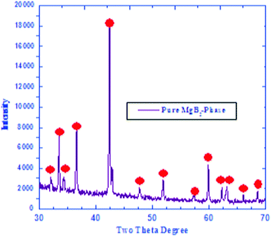 | ||
| Fig. 1 XRD curve recorded for synthesized pure MgB2. | ||
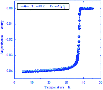 | ||
| Fig. 2 Magnetization curve recorded for synthesized pure MgB2. | ||
Here, we show that the high spatial compatibility of the 1 cm2MgB2 polished surface and graphene sheet makes it a perfect system to study the functional synthesis of multi-layer graphene on superconductor substrates by a injection–CVD process (ICVD). The high crystallinity, quality and large area growth of multi-layer graphene are desired as a resistive barrier for the formulated MgB2/Graphene/MgB2 junction. For CVD of the graphene layers, a freshly prepared 1 cm2MgB2 polished surface was heated and stabilized at the desired synthesis temperature. Then propylene gas (C3H6), see Fig. 3, which served as the carbon source, was introduced into the chamber. The gas pressure was adjusted to 3 × 10⁻⁶ mbar using a leak valve. In the incipient reaction of propylene with the 1 cm2MgB2 polished surface, a graphene monolayer is formed. This is evidenced by the appearance of a single π band in angle resolved photoemission spectroscopy (ARPES), as reported in29 and confirmed by both raman and STM-imaging of the honeycomb structure, see Fig. 4a,b. During the whole synthesis procedure, both the C3H6 gas pressure and the substrate temperature are monitored, and his complete set of information allowed us to monitor the full growth process dependent on time. The details of the CVD-synthesis is described elsewhere.21–24, 29
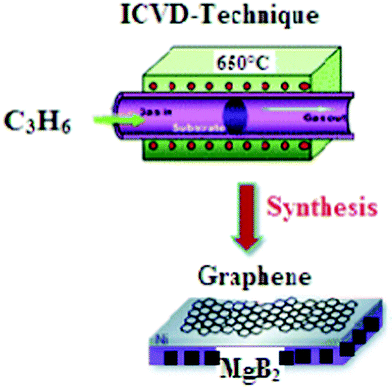 | ||
| Fig. 3 Schematic diagram represents the synthesis of multi-layered graphene using ICVD at a processing temperature of 650 °C and propylene gas as the carbon source. | ||
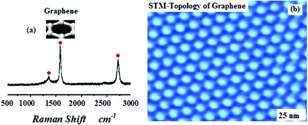 | ||
| Fig. 4 a, b: Characterisation of graphene by both raman spectroscopy and STM-imaging (Atomic Resolution mode) with honeycomb structure respectively. | ||
For this synthesis temperature (650 °C), the sample can be cooled down any time after the graphene layers are complete (i.e. t > 1600 s) without inducing a change in the graphene layer. This time of completion of one layer graphene is nearly double that recorded in29 due to our processing temperature (650 °C), which is lower than that reported in ref. 29, 900 °C.
Lowering the processing temperature is mainly to keep the crystal structure of the MgB2 superconductor substrate intact as it is by preventing the magnesium constituent from vaporization at higher temperatures. Finally the two identical MgB2 substrates loaded with a few layers of graphene are sandwiched together, as shown in Fig. 5, by compression using a hydrostatic compressor at 4 Ton cm−2 to formulate one junction tablet.
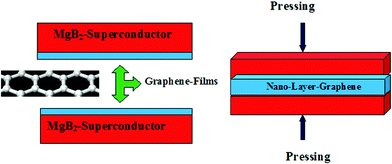 | ||
| Fig. 5 MgB2/Nano-Graphene/MgB2–Josephson Junction | ||
II.B. Nano/Micro structural features of the synthesized junction
Fig. 6a represents a high-resolution Atomic Force Microscopy (AFM) image captured with a Veeco-di Innova Model-2009-AFM-USA, for testing morphological features, and a topological map of the MgB2/Graphene/MgB2 junction surface by Tapping mode-Imaging. (Orange color = MgB2 and dark gray = graphene multi-layer). The thickness of the graphene barrier layer was found to be ∼ 0.1–0.35 μm, as clarified in Fig. 6b, which displays 3D-AFM imaging for a MgB2/Graphene/MgB2 junction surface with thickness ranging between 100–350 nm.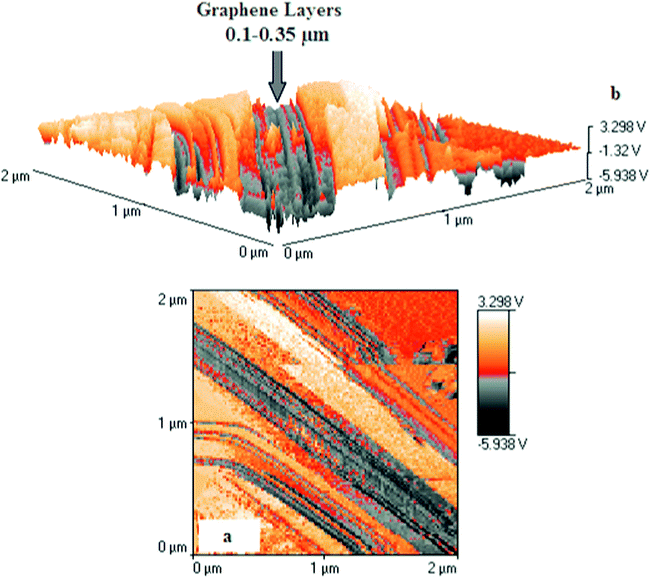 | ||
| Fig. 6 (a): High-resolution Atomic Force Microscopy (AFM) image captured with a Veeco-di Innova Model-2009-AFM-USA, for testing morphological features, and a topological map of the MgB2/Graphene/MgB2 junction surface by TappingMode-Imaging. (Orange color = MgB2 and dark gray = graphene multi-layer ∼ 0.1–0.35 μm). (b): 3D-AFM imaging for MgB2/Graphene/MgB2 junction surface using TappingMode-Imaging; Graphene layer represented by gray color with thickness ranging between 100–350 nm. | ||
The presently synthesized junction M-G-M exhibited a better binding adhesive strength (1.8–3.2 Å) than those reported in literature by Wintterlin et al.30 who stated that the average metal (substrate)–graphene spacing values ranged between 2.1–3.8 Å.
Fig. 7: (a and b): show scanning electron micrographs recorded for the MgB2/Graphene/MgB2 junction along the ab– and ba– perpendicular plane respectively, using a small piece (cut into very thin layer by diamond cutter) of the prepared junction (dark grey = graphene film and pale grey = MgB2 superconductor).
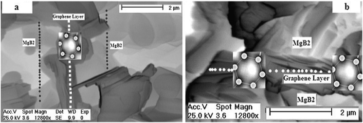 | ||
| Fig. 7 (a,b) Scanning Electron Microscope (SEM) image recorded for MgB2/Graphene/MgB2 junction along the ab– and ba– perpendicular plane respectively, using a small piece (cut into very thin layer by diamond cutter) of the prepared junction (dark grey = graphene film and pale grey = MgB2 superconductor) | ||
Finally we introduced a novel, simple technique to manufacture a MgB2/Graphene/MgB2 (MGM) junction as an electronic graphene superconducting quantum interference device, a powerful future platform for nanoscale magnetometry and fundamental transport studies. Tremendous investigations are needed from physicists to complete the image for this junction (MGM) as an electronic manufacture junction.
References
- K. S. Novoselov, A. K. Geim, S. V. Morozov, D. Jiang, Y. Zhang and S. V. Dubonos, Science, 2004, 306, 666–669 CrossRef CAS.
- C. Berger, Z. M. Song, X. B. Li, X. S. Wu, N. Brown and C. Naud, Science, 2006, 312, 1191–1196 CrossRef CAS.
- I. Meric, M. Y. Han, A. F. Young, B. Ozyilmaz, P. Kim and K. L. Shepard, Nat. Nanotechnol., 2008, 3, 654–659 CrossRef CAS.
- P. Avouris, Z. H. Chen and V. Perebeinos, Nat. Nanotechnol., 2007, 2, 605–615 CrossRef CAS.
- F. Schedin, A. K. Geim, S. V. Morozov, E. W. Hill, P. Blake and M. I. Katsnelson, Nat. Mater., 2007, 6, 652–655 CrossRef CAS.
- J. S. Bunch, A. M. van der Zande, S. S. Verbridge, I. W. Frank, D. M. Tanenbaum and J. M. Parpia, Science, 2007, 315, 490–493 CrossRef CAS.
- S. Niyogi, E. Bekyarova, M. E. Itkis, J. L. McWilliams, M. A. Hamon and R. C. Haddon, J. Am. Chem. Soc., 2006, 128, 7720–7721 CrossRef CAS.
- W. S. Hummers and R. E. Offeman, J. Am. Chem. Soc., 1958, 80, 1339 CrossRef CAS.
- T. Szabo, E. Tombacz, E. Illes and I. Dekany, Carbon, 2006, 44, 537–545 CrossRef CAS.
- G. I. Titelman, V. Gelman, S. Bron, R. L. Khalfin, Y. Cohen and H. Bianco-Peled, Carbon, 2005, 43, 641–649 CrossRef CAS.
- S. Stankovich, D. A. Dikin, G. H. B. Dommett, K. M. Kohlhaas, E. J. Zimney and E. A. Stach, Nature, 2006, 442, 282–286 CrossRef CAS.
- S. Stankovich, D. A. Dikin, R. D. Piner, K. A. Kohlhaas, A. Kleinhammes and Y. Jia, Carbon, 2007, 45, 1558–1565 CrossRef CAS.
- Z. F. Liu, Q. Liu, Y. Huang, Y. F. Ma, S. G. Yin and X. Y. Zhang, Adv. Mater., 2008, 20, 3924–3930 CrossRef CAS.
- Th. Seyller, K. V. Emtsev, K. Gao, F. Speck, L. Ley, A. Tadich, L. Broekman, J. D. Riley, R. C. G. Leckey, O. Radar, A. Varykhalov and A. M. Shikin, Surf. Sci., 2006, 600(18), 3906–3911 CrossRef CAS.
- K. S. Novoselov, P. Blake, R. Yang, S. V. Morozov, F. Schedin, L. A. Ponomarenko, A. A. Zhukov, R. R. Nair, I. V. Grigorieva and A. K. Geim, Solid State Commun., 2009, 149(27-28), 1068–1071 CrossRef.
- L. Xiaolin, Z. Guangyu, B. Xuedong, S. Xiaoming, W. Xinran, W. Enge and H. Dai, Nat. Nanotechnol., 2008, 3, 46 CrossRef.
- D. Mehandjiev, E. Bekyarova and M. Khristova, J. Colloid Interface Sci., 1997, 192(2), 440–446 CrossRef CAS.
- S. Stankovich, R. Piner, S. T. Nguyen and R. Ruoff, Carbon, 2006, 44(15), 3342–3347 CrossRef CAS.
- S.-H. Yeung, H.-K. Ng and K.-F. Man, AEU Int. J. Electron. Commun., 2008, 62(4), 266–276 CrossRef.
- K. Eisele, R. A. Gropeanu, C. M. Zehendner, A. Rouhanipour, K. Koynov, C. R. W. Kuhlmann, S. G. Vasudevan, H. J. Luhmann and T. Weil, Biomaterials, 2010, 31(33), 8789–8801 CrossRef CAS.
- A. Grüneis, M. H. Rümmeli, C. Kramberger, A. Barreiro, T. Pichler, R. Pfeiffer, H. Kuzmany, T. Gemming and B. Büchner, Carbon, 2006, 44(15), 3177–3182 CrossRef.
- A. Nagashima, N. Tejima, Y. Gamou, T. Kawai and C. Oshima, Surf. Sci., 1996, 357–358(20), 307–311 CrossRef CAS.
- M. Ishii, T. Meguro, T. Sugano, K. Gamo and Y. Aoyagi, Appl. Surf. Sci., 1995, 86(1–4), 554–558 CrossRef CAS.
- M. L. Ng, A. B. Preobrajenski, A. S. Vinogradov and N. Mårtensson, Surf. Sci., 2008, 602(6), 1250–1255 CrossRef CAS.
- M. Rigaud, G. Giovannetti and M. Hone, J. Chem. Thermodyn., 1974, 6(10), 993–998 CrossRef CAS.
- E. Loginova, F. Cosandey and T. E. Madey, Surf. Sci., 2007, 601(3), L11–L14 CrossRef CAS.
- C. Thirion, W. Wernsdorfer, M. Jamet, V. Dupuis, P. Mélinon, A. Pérez and D. Mailly, J. Magn. Magn. Mater., 2002, 242–245(2), 993–995 CrossRef CAS.
- C. Aglar Girit, V. Bouchiat, O. Naaman, Y. Zhang, M. F. Crommie, A. Zettl and I. Siddiqi, Nano Lett., 2009, 9, 198–199 CrossRef.
- A. Grüneis, K. Kummer and D. V. Vyalikh, New Journal of Physics, 2009, 11 Search PubMed.
- J. Wintterlin and M. L. Bocquet, Surf. Sci., 2009, 603(10–12), 1841–1852 CrossRef CAS.
| This journal is © The Royal Society of Chemistry 2011 |