
 Open Access Article
 This Open Access Article is licensed under a
 Creative Commons Attribution 3.0 Unported Licence
Development and optimisation of a SiO2 PVD technique based on the thermal decomposition of PDMS†
Paul
Cannon
 *a,
Enda
McGlynn
ab,
Brian
Freeland
c and
Jennifer
Gaughran
a
*a,
Enda
McGlynn
ab,
Brian
Freeland
c and
Jennifer
Gaughran
a
aSchool of Physical Sciences, Dublin City University, Dublin 9, Ireland. E-mail: paul.cannon3@mail.dcu.ie
bNational Centre for Plasma Science and Technology, Dublin City University, Dublin 9, Ireland
cSchool of Biotechnology, Dublin City University, Dublin 9, Ireland
First published on 12th January 2023
Abstract
This work reports the development of a novel and facile physical vapour deposition (PVD) system for SiO2 deposition with a wide and controllable range of final film thicknesses. An investigation of the steady-state deposition temperature, heating rate, and PDMS source mass dependence of the deposited SiO2 layer thickness was performed using a variety of experimental techniques. SiO2 layers were characterised by scanning electron microscopy (SEM), energy dispersive x-ray spectroscopy (EDX), x-ray photoelectron spectroscopy (XPS), grazing incidence attenuating total reflection Fourier transform infrared spectroscopy (GATR-FTIR), contact profilometry (CP), and white light profilometry (WLP). It was found that the thickness of the SiO2 layer was linearly proportional to the PDMS source mass for large source masses with a nonlinear (parabolic) relationship for smaller source masses, but a non-monotonic relationship was observed between thickness and source material heating rate. The steady-state deposition temperature above the decomposition threshold did not directly affect layer thickness within the range investigated but, the lower the temperature, the greater the film uniformity.
Introduction
Silicon dioxide (silica or SiO2) has a broad range of applications throughout many industries. In the electronics industry, it is the most widely used dielectric as a gate insulator for field-effect transistors (FETs) due to its high resistivity, dielectric strength, large band gap, and high melting point.1,2 Silica is also widely utilised in biomedical diagnostics, where it is employed in the current state-of-the-art technique for DNA isolation and purification.3 This technique utilises the affinity between silica surfaces and proteins/nucleic acids.4 Silica thin films have been deposited on various structures including silicon micropillars for enhanced DNA capture,5,6 and on gold/noble metal surfaces to bind molecules for low cost surface plasmon resonance detection methods.7,8 Historically, SiO2 deposition was performed at high temperatures and was based on the pyrolysis of silane in the presence of oxygen at atmospheric pressure.9 As computer components increased in complexity, electronic layers required more uniform, conformal, and controllable layer deposition at lower temperatures (less than the ∼900 °C used in traditional chemical vapour deposition (CVD)), in order to not adversely affect underlying layers in multilayer structures and to reduce long processing times. Additionally, high temperature deposition may not be suitable for all substrates, especially when it comes to low-cost substrates like quartz crystal microbalances for point-of-care medical applications. These quartz crystals have a phase transition temperature of 573 °C, after which they no longer function as a resonator.10 Low pressure CVD (LPCVD) was developed to significantly increase film uniformity and conformity, but it still requires high temperatures. Plasma enhanced CVD (PECVD) was invented to satisfy both criteria, as the plasma conditions alter the thermodynamics of surface reactions, considerably lowering the temperature at which reactions are possible, allowing for much lower temperature deposition with superior uniformity.11,12 However, each CVD technique comes with significant drawbacks, with CVD providing low step coverage, LPCVD requiring high temperatures, and PEVCD requiring constant chamber cleaning due to risks of contamination from particle build-up, and all of these techniques requiring expensive and highly toxic precursor gases, usually silane.13 We also note that thin films of a range of other metal oxide materials are being studied for a variety of applications, including as gate oxides in FET structures.14–17Many alternative techniques have been developed to improve individual aspects of the SiO2 deposition process, such as sol-gel processes,18 magnetron sputtering,19 electron beam deposition,20 with the most promising being atomic layer deposition (ALD).21 ALD provides unrivalled step coverages and conformity/uniformity, allowing controllable sub-nanometre thicknesses with pinhole free layers due to the atomic layer by layer growth mechanism.22,23 However, this comes with a time, instrumentation and material cost, with significantly increased processing times and very low material and energy utilization efficiency.24
In addition, low pressure and vacuum-based technologies come with high manufacturing costs, which is further increased when attempting to accommodate large area depositions. Thus, research into lower cost and scalable deposition techniques have gained increased focus in recent years. Physical vapour deposition (PVD) has emerged as a lower cost, and safer alternative to other deposition techniques. PVD shares many similarities with CVD, but the differences occur in the precursor materials.25 CVD utilises precursor gas/gases which initiate chemical reactions near or on the heated substrate surfaces, producing chemical by-products, resulting in by-product deposition on the substrate while other by-products and unreacted precursor gases are exhausted out of the reaction chamber. PVD is a much simpler process, involving the thermal evaporation of a precursor material to produce a vapour phase. The vapour atoms are transported, typically through a low pressure zone in a straight line path, and deposit directly on the substrate.26 The aforementioned magnetron sputtering, and e-beam evaporation methods are examples of PVD techniques, with the former a plasma-based technique, and the latter a high-power technique, both requiring high vacuum environments.
In this report we demonstrate a low-cost, facile, and novel experimental setup for SiO2 thin film PVD under atmospheric pressure at relatively low temperatures using small amounts of precursor source material. Our work modifies the experimental conditions created by Hu et al.,27 and is based on the thermal degradation mechanisms of polydimethylsiloxane (PDMS) investigated by Camino et al.28,29 That is, PDMS thermally decomposes at temperatures above ∼450 °C, into volatile cyclic oligomers. In air, these volatile oligomers become oxidised, leading to the formation of gaseous SiO2 species that nucleate and grow heterogeneously on the surface of solid substrates. SiO2 films were deposited on p-type Si wafers, and the influence of heating rate, steady-state deposition temperature, and mass of PDMS on the final film thickness was studied for the first time. The thickness can be precisely controlled by changing either the amount of PDMS precursor material or the heating rate used to reach the steady-state deposition temperature, or both. The lower the steady-state deposition temperature is, above the PDMS decomposition threshold, the greater the film uniformity.
Materials and methods
Synthesis of PDMS
Thin films were deposited via thermal evaporation of PDMS. PDMS was synthesised using the Sylgard 184 silicone elastomer kit from Dow Corning Corporation. The PDMS base and curing agent were mixed in a 10![[thin space (1/6-em)]](https://www.rsc.org/images/entities/char_2009.gif) :1 ratio by weight, respectively, and allowed to cure at room temperature for at least 48 hours.
:1 ratio by weight, respectively, and allowed to cure at room temperature for at least 48 hours.
PVD configurations
The first configuration adopted the setup of Hu et al.27 The PDMS block was loaded into an alumina boat and the substrate was placed vertically above the PDMS, across the top opening of the boat. This boat, containing both PDMS and substrate, was placed in a Nabertherm Muffle Furnace LT 3/11/B410 and heated in air to 650 °C (the steady-state deposition temperature) at a rate of 12 °C minute−1, remaining at this temperature for 2 hours.The second configuration utilised the same apparatus as configuration one, however the sample was placed downstream along the alumina boat, with a lateral distance of ∼5.5 cm from the PDMS block.
The third and final configuration was identical to configuration two, except the entire alumina boat containing PDMS and substrate was placed within a hollow quartz tube of 3.8 cm inner diameter. The tube was pointed towards the furnace exhaust, with the substrate positioned between the PDMS block and exhaust (Fig. 1). This configuration was utilised for the entire subsequent investigations of the influence of PDMS mass (1.5–48 mg), steady-state deposition temperature (450–650 °C), and heating rate (1–40 °C minute−1) on SiO2 deposition thickness.
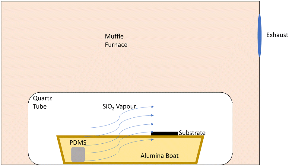 | ||
| Fig. 1 Schematic diagram of novel PVD system for SiO2 deposition on solid substrates. The substrate is placed between the heated block of PDMS and the exhaust of the muffle furnace, utilising the difference in temperature to drive the SiO2 vapour over the substrate. The quartz tube ensures most of the vapour is directed over the substrate, providing more controlled deposition. | ||
Film characterisation
SiO2 films were imaged using a Karl-Zeiss EVO 50 series scanning electron microscope (SEM) with an Oxford Instruments Xplore detector mounted within to provide additional chemical information via energy dispersive x-ray spectroscopy (EDX).Further chemical properties were characterised by grazing-angle attenuated total reflection Fourier Transform Infrared Spectroscopy (GATR-FTIR) using a Nicolet iS50 FTIR equipped with a Harrick VariGATR attachment, and X-ray photoelectron spectroscopy (XPS) using a Scienta Omicron X-ray photoelectron spectrometer with a monochromated Al Kα source (1486.7 eV) and a 128 channel Argus CU detector. FTIR measurements were taken from an average of 128 scans with 8 cm−1 resolution, using a force of ∼700 N, for an optimum signal to noise ratio as per manufacturer specifications for measuring thin films on silicon. XPS measurements were taken using a 0.1 eV step size.
Film thicknesses were determined using a Bruker Dektak XT Profilometer with a 2.5 µm radius stylus. Scan parameters varied depending on sample and scan length, but all scan speeds were ≤100 µm s−1 and were generally chosen to produce 300 nm per pt resolutions. CP data was filtered using a two-sided (±10 µm) moving average to better illustrate the average thicknesses, but the raw data can be found in the ESI.† Grey highlighted areas in the CP measurements indicate uncoated substrate regions, and blue highlighted areas indicate where the average thickness measurement was taken from. The average thickness measurements were taken from the areas of the sample located along the centre of the alumina boat. These measurements were supported by white light profilometry (WLP) measurements using a Bruker Contour GT Profilometer. Due to the transparent nature of the thinner SiO2 films (<200 nm), gold coating was required for WLP measurements. Gold coating was carried out in an Edwards AUTO 306 Vacuum Coater, using a tungsten filament operated under a ∼1.5 kV voltage and ∼20 mA current, to produce a 24.6 nm reflective layer on top of the SiO2 which was monitored and confirmed by a resonating crystal detector within the instrument.
Results and discussion
Development and optimisation of PVD system
Firstly, we sought to achieve coatings similar to the technique described by Hu et al. using the same experimental setup and conditions.27 However, it is important to note that they were coating only the internal walls of a porous anodic aluminium oxide template, which would allow only a fraction of the vapour to enter and coat the nanopores, whereas we wished to coat the surfaces of solid, nonporous substrates. This setup labelled “configuration one” from this point onwards, resulted in coatings that were millimetres, rather than nanometres, thick (Fig. 2). This is because our nonporous substrate caused build-up of the material due to its impermeable nature and close proximity to the vapour source. Additionally, we found that the PDMS expands greatly and physically came into contact with the substrate, which drastically reduced the quality of the deposited coating, as shown in Fig. 2. | ||
| Fig. 2 Photograph of SiO2 deposition following the procedure of Hu et al.,27i.e. configuration one, showing the thick coatings and expansion of PDMS during heating. | ||
To overcome the issues of PDMS expansion, and to reduce the coating thickness, we developed configuration two. Configuration two was the same as configuration one (Fig. 2), except the PDMS was placed at one end of the alumina boat, and the substrate was placed at the opposite end, rather than directly on top of one another. However, while this produced a significantly thinner coating, it was entirely uneven across the sample surface (Fig. 3a). The work reported by Favors et al.30 however adopted a similar deposition technique, where they used a tube furnace, sub-atmospheric pressures, and controlled gas flows to produce nanometre thickness coatings and circumvent the aforementioned problems of the technique of Hu et al.27 Their technique also required significantly less PDMS, using 50 mg compared to the 600 mg used in the original work. We modified the approach of Favors et al.30 to one which requires neither a tube furnace nor sub-atmospheric pressures and controlled gas flows to achieve conformal nanometre coatings by using a standard muffle furnace/oven, open to air at atmospheric pressure, as described in the materials and methods. By simply placing the alumina boat containing PDMS with the sample downstream, all inside a hollow cylindrical quartz tube with similar length to the alumina boat (Fig. 1), the vapour is directed entirely over the sample surface, resulting in more deposition and uniformity of SiO2, as seen in Fig. 3c.
 | ||
| Fig. 3 (a) Photograph of SiO2 deposition by PVD configuration two i.e., alumina boat without quartz tube. (b) SiO2 film thickness measurements across samples (a) and (c). (c) Photograph of SiO2 deposition by configuration three i.e., the alumina boat contained within a hollow quartz tube configuration. Both depositions were carried out under the same conditions (∼47.5 mg PDMS, 650 °C steady-state deposition temperature, 12 °C min−1 heating rate). | ||
Given that the entire vapour is confined and directed over the sample, the coating was much thicker than it was when using the same setup without the quartz tube (configuration two), going from an average thickness of 500 nm to ∼1700 nm in the central regions (Fig. 3b). The configuration three results show full sample coverage when compared to the technique performed without the quartz tube in configuration two, however the profilometry results show large variations in thickness of the order of microns over length scales of microns. The contact profilometry results in isolation would suggest the quartz tube gives rise to significantly poorer quality coatings, but the visual images show a clear difference in sample coverage and uniformity on the scale of centimetres (Fig. 3). The results prompted us to continue with the quartz tube method, and to significantly reduce the amount of PDMS used.
The sample grown using configuration three was imaged under SEM (Fig. 4) to better understand the large roughness observed in Fig. 3. EDX was also performed to confirm that we were indeed obtaining a pure SiO2 coating. By using a relatively low accelerating voltage (9.00 keV) in combination with the ∼micron thickness of the coating, we obtained EDX spectra without substrate contamination due to a ∼300 nm penetration depth for the primary electron beam. The SEM image in Fig. 4a shows clear island growth which is consistent with the contact profilometry results observed. Calculating the atomic percentages from the weighted EDX results in Fig. 4b gives a 69.3%:30.7% or 2.26:1 ratio of oxygen to silicon, which is again consistent with the result expected for silicon dioxide and is in agreement with the values obtained by Favors et al.30 The coating in Fig. 4 shows large, spherical island features. These may indicate that the SiO2 preferentially homogenously nucleates on already deposited SiO2. If these features are present on the thinner coatings discussed later, they cannot be seen by SEM.
 | ||
| Fig. 4 (a) SEM image of the sample grown using 47.5 mg of PDMS via configuration three, as shown in Fig. 3c. The coating displays island-type growth, characteristic of SiO2 on Si using PVD, with individual islands of ∼1 µm in size, alongside multi-island structures. (b) EDX spectra of the same sample imaged in (a) showing the weight percentages of Si and O signals. | ||
Film thickness vs. PDMS mass
Hu et al.27 found that the SiO2 thickness was linearly proportional to the amount of PDMS used, so the next step was to significantly reduce the amount of PDMS used in the process to produce thinner coatings of nanometre dimensions. We performed depositions using 47.5, 30.6, 12.0, 6.0, and 1.5 mg of PDMS source material and measured the resulting thicknesses. The results are shown in Fig. 5. | ||
| Fig. 5 Film thickness vs. PDMS mass using a 12 °C min−1 heat rate, and a steady-state deposition temperature of 650 °C. The red line is a guide to the eye, using a parabolic form with a constant offset. | ||
A rough linear trend in thickness versus source material mass is seen for source masses of 47.5, 30.6 and 12.0 mg. However, there is only a 4% reduction in film thickness when reducing the PDMS mass from 6.0 to 1.5 mg. This result was replicated four times and similar behaviour was seen on each occasion. A nonlinear relationship is seen for smaller source masses, with the film thickness seeming to plateau at 6 mg of PDMS and below. This reasoning for this result was not clear initially, so we opted to investigate the influence of both furnace steady-state deposition temperature and heating rate on the resultant film thickness to shed some light on the process.
Film thickness vs. steady-state deposition temperature
Keeping the mass of PDMS constant at 12 mg, we initially performed the SiO2 deposition using a large range of steady-state deposition temperatures (450–650 °C, in 50 °C intervals). The lower point of the range chosen was the minimum threshold temperature required to initiate the degradation mechanism for PDMS, and the largest temperature was the one used by both Hu et al.27 and Favors et al.30 Each sample was heated at a rate of 12 °C minute−1 and maintained at the steady-state temperature for two hours to ensure complete degradation of PDMS, and the results can be seen in Fig. 6. | ||
| Fig. 6 Steady-state deposition temperature dependence of SiO2 film thickness using 12 mg of PDMS at a heating rate of 12 °C minute−1. | ||
Fig. 6 shows the effect of the steady-state temperature on the SiO2 deposition process. The most obvious result is that lower temperatures give much less surface roughness, although the coatings themselves do not visually appear flat and are continuing to increase in thickness across the substrate, whereas the higher temperature samples have much rougher surfaces, but the thicknesses seem to plateau. Surface roughness measurements, as determined by the Dektak XT software, give surface roughness values of 34.7, 15.8, 16.9, 8.3, and 0.4 nm from higher to lower temperature, with the bare Si wafer reference sample (with no deposition) having a roughness of 0.1 nm.
The observed film increase in thickness of SiO2 deposition across individual samples appears to be due to the influence of the piece of bare Si placed on top of the sample surface in order to provide an uncoated area to use as a point of reference for the coating measurements. This is used to provide a flat measurement of the bare Si surface, and this “marked” region can be seen as the flat region highlighted in grey on the left-hand side of Fig. 6. The higher temperature coatings appear relatively unaffected by this, given the step edge between the flat region and the coated region. We see more gradual changes between the flat and coated regions at lower temperatures. We believe the large Si piece is deflecting the vapour more at lower deposition temperatures, causing thicker coatings to occur as the distance is increased from this piece.
In order to test this hypothesis, we performed a 500 °C deposition without this Si piece (Fig. 7) and the SiO2 film was quite flat compared to the data illustrated in Fig. 6, showing only an average 50 nm increase in thickness in the substrate centre. The thickness increases between 5–15 mm correspond to the area of the wafer directly above the alumina boat. These positions are where the silicon contacts the boat, so it is expected that we would see an increase in coating thickness in the centre of the boat.
 | ||
| Fig. 7 SiO2 coating without Si piece to mark uncoated areas alongside a scan across the same sample after the “Scotch-Tape” test performed on the latter half of the surface (10–20 mm). | ||
We also performed the standard “Scotch Tape” test (Fig. 7) on this same sample to qualitatively measure the strength of adhesion, alongside repeated washing with isopropyl alcohol and deionised water, and the coating appeared unaffected, indicating good adhesion. A sticky residue remained after the test, which can be seen on the right-hand side of the profilometry data of Fig. 7. For all subsequent tests, this Si piece was cleaved to be as small as possible and the substrates to be coated were increased in length from their initial size, equal to the width of the alumina boat (1–1.2 cm), to over double the width (2.5 cm) of the boat in order to have the Si piece as far from the boat centre as possible.
By applying the above sample modifications, we performed further depositions between 460–500 °C using only 6 mg of PDMS (Fig. 8). We observe no evidence of SiO2 deposition at 450 °C because this is the threshold temperature required for the bond scission of cyclic oligomers. This temperature must be exceeded to generate the SiO2 vapour. Fig. 8a shows there is no significant dependence of the film thickness on the steady-state deposition temperature in this temperature range. Findings from Camino et al.28 suggest that there could be a temperature dependence, as the weight of the PDMS block gradually decreases with increasing temperature after thermal degradation begins, until it eventually plateaus at a higher temperature. However, we maintain the steady-state deposition temperature for two hours, whereas they measured the change in mass with increasing temperature without maintaining each temperature for a set amount of time. Our lower temperature deposition for longer periods of time may be broadly equivalent to increasing the temperature until the PDMS has been completely degraded. The steep incline seen at the left-hand side of Fig. 8a (∼2–7.5 mm) occurs between the silicon piece and the nearest contact point between the sample Si and the alumina boat, and the flat central region of the coating (∼7.5–15 mm) corresponds to the centre of the alumina boat (illustrated in Fig. 8b). The thickness of the coating begins to vary beyond this, starting roughly at the second contact point between sample and alumina (located at ∼15 mm), and continuing along the sample in the region overhanging the alumina. We believe the upward thickness trend after the horizontal position labelled 15 mm onwards seen for some of the samples is a result of a slight tilt of the sample/boat during the deposition process.
 | ||
| Fig. 8 (a) Steady-state deposition temperature dependence of SiO2 coating using 6 mg PDMS at a heating rate of 12 °C minute−1 using updated sample preparation. (b) Annotated top-down photograph of SiO2 PVD sample highlighting the different coating regions observed in (a). | ||
With this updated sample preparation, we performed a deposition at 500 °C and 650 °C using 1.5 mg of PDMS to compare the impact of steady-state deposition temperature on SiO2 film thickness over a large temperature range. Fig. 9 shows very similar thicknesses at each temperature across a 1.6 cm long substrate, with the higher temperature deposition showing an increased surface roughness, which was to be expected based on the results shown in Fig. 7 and 8. These data further strengthen our conclusions based on the earlier data.
 | ||
| Fig. 9 SiO2 coating at steady-state deposition temperatures of 500 °C and 650 °C, each using 1.5 mg of PDMS and a heating rate of 12 °C minute−1. | ||
Film thickness vs. heating rate
While flat and uniform coatings were being produced, they were still ∼200 nm thick. To further reduce the coating thicknesses, we reviewed the work done by Camino et al., who studied the thermal degradation mechanisms/kinetics of PDMS.28,29 They discovered that the products of the thermal degradation of PDMS depend on the heating rate, as this strongly affects the degree of depolymerization. Lower heating rates and steady-state temperatures produce the volatile cyclic oligomers required as the precursors for SiO2 vapour generation. However, the lower the heating rate is, the lower the degree of depolymerization is and hence less SiO2 vapour will be produced in this case. Rapid heating rates result in increased depolymerization, but these cyclic oligomers are then accompanied by linear oligomers, with the latter dominating the reaction products. Here, a radical mechanism occurs through homolytic Si–CH3 bond scission. Cross-linking of macro-radicals here decreases the flexibility of the PDMS chain and hinders the splitting of cyclic oligomers. So rather than getting more SiO2 vapour, bond reorganisation takes place with the formation of ceramic silicon–oxycarbide, which represents the majority of the reactant product, producing less SiO2 vapour.We performed SiO2 coating at three different heating rates under a steady-state deposition temperature of 500 °C; the original 12 °C minute−1 used by Hu et al.27 and Favours et al.,30 and also at the minimum (1 °C minute−1) and maximum (40 °C minute−1) rates achievable with our system. We can clearly see this non-monotonic relationship in Fig. 10, with 1 and 40 °C minute−1 heating rates producing significantly thinner coatings than a heating rate of 12 °C minute−1. The film thickness for the 1 °C minute−1 deposition peaks at 60 nm and ranges consistently between 25–50 nm in the centre of the boat. These results provide additional context for those observed during the film thickness vs. PDMS mass investigation. The 1.5 mg blocks of PDMS are very small, with a significantly higher surface to volume ratio than the other blocks used. These smaller blocks undergo more rapid depolymerisation at high heating rates as a result of their small size and high surface to volume ratio, resulting in an altered reactant product compared to the larger masses. The 1 °C minute−1 heating rate depositions were repeated to demonstrate the reproducibility of the PVD system, and the results in Fig. 11 demonstrate good process reproducibility.
 | ||
| Fig. 10 SiO2 thickness dependence on heat rate for a steady-state deposition temperature of 500 °C using 6 mg of PDMS. | ||
 | ||
| Fig. 11 Profilometry scans of three different substrates subjected to SiO2 PVD using 6 mg PDMS and 1 °C minute−1 heat rates using a steady-state deposition temperature of 500 °C, demonstrating the process reproducibility for deposition of very thin films across a large area along the centre of the alumina boat. (Inset; Higher magnification view of the SiO2 thickness across a 50 µm long region on the sample). | ||
Considering the results of each deposition parameter, alongside the thermogravimetric analysis of PDMS at different heating rates performed by Camino et al.,28 the effect of steady-state deposition temperature on film thickness is likely more apparent at lower heating rates than the 12 °C minute−1 utilised here. At large heating rates, there is rapid degradation of PDMS per unit temperature above the decomposition threshold, whereas slower heating rates show a much lower amount of degradation per unit temperature, with two distinct stages of degradation emerging. However, we choose not to investigate this due to the tunability already available from varying the PDMS mass and heating rate alone.
In addition, characterisation via WLP was carried out to complement the CP measurements. The WLP results of the 1 °C minute−1 heat rate sample can be seen in Fig. 12, and it shows very good agreement with the data of Fig. 10 and 11. Due to the transparent nature of the SiO2 film, secondary fringes would occur due to reflections from the top of the film, as well as from reflections from the silicon wafer surface which arose from white light transmitted through the film. For this reason, a thin (∼25 nm) layer of gold was deposited on top of the SiO2 film to attenuate the white light and prevent these secondary transmission fringes from occurring. The gold layer was deposited by e-beam evaporation to better maintain the SiO2 surface topography compared to other sputter coating techniques. The gold layer was slightly thinner at the step between uncoated Si and SiO2 which can be seen as a sharp increase in thickness around the 1600 µm position. Comparing the heights between the uncoated Si and the centre region of the SiO2 coating, we obtain a film thickness measurement of 79.6 nm, which, when corrected for the gold layer thickness, gives a thickness of 55.0 nm, in excellent agreement with the CP results. The uniformity of the SiO2 film thickness was determined to be less than 1.0 nm both transversely and longitudinally across the entire region imaged in Fig. 12a. The periodic peaks and troughs which occur in the CP data were also present in the line profiles of the WLP data, with similar widths of 500 microns. The periodic peaks and troughs also occur in the uncoated regions of the SiO2 coated samples, as well as the untreated Si substrates. The presence of these similar features in each set of measurements made by two different techniques indicates they are characteristics of the Si substrate rather than the SiO2 coating. The gold coated SiO2 film was also imaged via SEM and can be seen in Fig. 12b–e. The top-down view images (Fig. 12b and c) verify the uniformity of the film due to the lack of contrast seen in the images. Small surface topographical features (Fig. 12c) can be seen on some areas of the film, but these occurred relatively infrequently. Cross-sectional (at 90°) images of the sample labelled 2 in Fig. 12 can be seen in Fig. 12d and e, which show very good agreement between the film thicknesses determined by both techniques. The coating in the centre of the substrate (Fig. 12d) corresponds to (90 ± 20) nm, which, when corrected for the additional ∼25 nm of gold, is in very good agreement with the results shown in Fig. 11. Fig. 12e shows the decreased thickness of the film (45 ± 10 nm including the ∼25 nm gold contribution) outside the central region of the sample, in this case at a position of approximately 5 mm along the substrate (see Fig. 11 also).
 | ||
| Fig. 12 (a) WLP measurement of the same SiO2 sample deposited using 6 mg PDMS and a 1 °C minute−1 heat rate shown in Fig. 10. The sharp step seen around the 1600 µm position (indicated by the red asterisk) is due to the large change in reflection due to the 24.6 nm gold coating on top of the transparent SiO2 film, and secondary interference fringes occurring here due to a slightly decreased gold layer thickness at the step edge. (b)–(e) SEM images of sample 2 in Fig. 11. (b) Top-down view of the SiO2 coating, showing the gold coating (left) and the SiO2 without gold coating (right). (c) Top-down view of the SiO2 coating, showing <200 nm sized surface topographical features on the surface. (d) Cross-sectional (90°) view of the Au-SiO2 coating in the centre of the substrate with an average thickness of (90 ± 20) nm (e) Cross-sectional (90°) view of the region of the Au-SiO2 coating away from the centre (at a position of approximately 5 mm along the substrate) with an average thickness of (45 ± 10) nm. | ||
Lastly, the thinner SiO2 samples were analysed using XPS and GATR-FTIR spectroscopy, to determine physical and chemical characteristics that could be not measured by EDX. GATR-FTIR data (Fig. 13) shows the increased intensity of the symmetric and asymmetric stretching vibrations of Si–O–Si, at 800 and 1100 cm−1 respectively, indicative of the presence of an increased deposit of SiO2 in the thickest sample. The sharp peak at 1250 cm−1 observed in the uncoated Si sample is caused by longitudinal optical phonons of the crystalline silicon wafer and its native oxide.31,32 While GATR-FTIR is useful for detecting chemical bonds in our samples, we looked at XPS for chemical identification for very thin films, and to better distinguish between Si and SiO2.
 | ||
| Fig. 13 (a) FTIR spectra of the SiO2 coatings at varying thicknesses, showing the symmetric and asymmetric stretching vibrations of Si–O–Si at 800 and 1100 cm−1 respectively, and longitudinal optical phonons of the crystalline silicon wafer and its native oxide at 1250 cm−1 in the uncoated substrate. | ||
Fig. 14 shoes the XPS data for the Si 2p and O 1s orbital regions, with the Si 2p bulk signal occurring at the expected 99.4 eV position and decreasing with increasing SiO2 thickness until it becomes completely obscured by the overlying coating.33 In parallel, we see the characteristic SiO2 2p intensity (104 eV) increase with increasing thickness, and we also see the binding energy of this feature increase compared to the expected 104 eV energy. This shift is due to surface charging effects which occur as photoelectrons are emitted from the SiO2 layer (34). As SiO2 is insulating, it cannot readily replace emitted electrons, causing a build-up of positive charge which increases the binding energy of remaining electrons. This phenomenon is more pronounced in the thicker coatings. We also performed a 50 nm SiO2 coating on conductive ZnO nanostructures, and the binding energy decreases from 105.3 eV when grown on the native insulating oxide of Si, to 104.6 eV, supporting our identification of this energy shift as being due to charging and not the generation of other oxidation states. This is further supported by the corresponding O 1s spectra, where similar shifts due to surface charging are observed in these samples. We note that we still see some evidence of the Si 2p bulk signal in the 50 nm coating spectra, although the elastic mean free path should be no greater than 10 nm. This substrate signal may be due to emission from more thinly coated regions of the sample, or from small pinholes that CP cannot detect due to the large tip diameter (5000 nm) relative to the nanometre dimensions of the coating features. The SEM image in Fig. 4 shows the non-uniform nature of micron scale coatings, with apparent “gaps” between large island-like features which may still be present on a significantly reduced scale in the thinner coatings.
 | ||
| Fig. 14 XPS spectra of SiO2 coatings of varying thicknesses of the (a) Si 2p region showing the decrease in Si signal (99.4 eV) and increasing oxide signal (104+ eV) with increasing SiO2 thickness, and the (b) O 1s region showing the increasing O signal (∼533 eV) with increasing SiO2 thickness. Both spectra show surface charging effects. | ||
Conclusions
We have demonstrated a novel and facile PVD setup for the controllable deposition of very thin SiO2 films on solid substrates under atmospheric pressure at relatively low temperatures. Our system allows deposition of a wide range of film thicknesses utilising very small amounts of PDMS rubber in a fast and cost-efficient manner. The deposited film thickness can be tightly controlled by varying the deposition temperature, the amount of PDMS used, as well as the heating rate, with more uniform depositions achieved at lower temperatures. Reproducible SiO2 layers as thin as 25–50 nm were achievable as a result of this investigation, while also achieving much thicker coatings of 50 to greater than 2000 nm. Our work investigated three of the critical factors relevant to the deposition process and deposited film parameters and thus provides an important starting point for the further exploration and exploitation of the process.In addition, our process set-up and subsequent investigations provide a blueprint for performing depositions on substrates and nanostructures susceptible to deformation or other adverse effects at high temperatures and/or under high heating rates. The depositions achievable at low temperatures and low heating rates show our system to be highly compatible with a diverse array of substrates including flexible substrates and nanostructured substrates.
Future work will involve PVD deposition of SiO2 on ordered, high aspect ratio nanostructures to produce uniform and conformal coatings. Preliminary work has shown this technique to be capable of coating 400 nm tall nanorods with good conformality, and the SiO2 coating displays DNA binding capabilities in controlled tests. We hope to then utilise these coated nanostructures for biomedical diagnostic applications.
Author contributions
Paul Cannon: Methodology, validation, formal analysis, investigation, data curation, writing – original draft, visualization, funding acquisition. Enda McGlynn: conceptualization, methodology, resources, writing – review & editing, supervision, funding acquisition. Brian Freeland: writing – review & editing, supervision. Jennifer Gaughran: conceptualization, methodology, resources, writing – reviewing & editing, supervision, funding acquisition.Conflicts of interest
There are no conflicts to declare.Acknowledgements
The research conducted in this publication was funded by the Irish Research Council under the Government of Ireland Postgraduate Scholarship Programme [grant number: GOIPG/2021/379]. The authors would like to thank Dr Robert O’Connor and Mr Darragh O’Neill from the School of Physical Sciences in Dublin City University, for the use of their XPS system and for performing the XPS measurements respectively, Dr Barry O’Connell from the Nano Research Facility in Dublin City University for extensive and highly expert assistance with WLP measurements, and Ms Erin Rouse for repeating some depositions and enabling further analysis. The CP, WLP and XPS measurements were carried out at the Nano Research Facility in Dublin City University which was funded under the Programme for Research in Third Level Institutions (PRTLI) Cycle 5. The PRTLI is co-funded through the European Regional Development Fund (ERDF), part of the European Union Structural Funds Programme 2011–2015.References
- M. L. Green, E. P. Gusev, R. Degraeve and E. L. Garfunkel, Ultrathin (<4 nm) SiO2 and Si–O–N gate dielectric layers for silicon microelectronics: Understanding the processing, structure, and physical and electrical limits, J. Appl. Phys., 2001, 90(5), 2057 CrossRef CAS.
- H. G. P. Lewis, et al., “The silicon-silicon dioxide system: Its microstructure and imperfections, Rep. Prog. Phys., 1994, 57(8), 791 CrossRef.
- R. Boom, C. J. A. Sol, M. M. M. Salimans, C. L. Jansen, P. M. E. Wertheim-Van Dillen and J. Van Der Noordaa, “Rapid and simple method for purification of nucleic acids, J. Clin. Microbiol., 1990, 28(3), 495–503 CrossRef CAS PubMed.
- B. Shi, Y. K. Shin, A. A. Hassanali and S. J. Singer, “DNA Binding to the Silica Surface, J. Phys. Chem. B, 2015, 119(34), 11030–11040 CrossRef CAS PubMed.
- N. C. Cady, S. Stelick and C. A. Batt, “Nucleic acid purification using microfabricated silicon structures, Biosens. Bioelectron., 2003, 19(1), 59–66 CrossRef CAS PubMed.
- L. A. Christel, K. Petersen, W. McMillan and M. A. Northrup, “Rapid, Automated Nucleic Acid Probe Assays Using Silicon Microstructures for Nucleic Acid Concentration, J. Biomech. Eng., 1999, 121(1), 22–27 CrossRef CAS PubMed.
- D. K. Kambhampati, T. A. M. Jakob, J. W. Robertson, M. Cai, J. E. Pemberton and W. Knoll, “Novel silicon dioxide sol-gel films for potential sensor applications: a surface plasmon resonance study, Langmuir, 2001, 17(4), 1169–1175 CrossRef CAS.
- A. Renier, T. Mangeat, H. Benalia, C. Elie-Caille, C. Pieralli and B. Wacogne, “Gold/silica thin film for biosensors applications: Metal enhanced fluorescence, Laser Phys., 2010, 20(3), 591–595 CrossRef CAS.
- J. Foggiato, “Chemical Vapor Deposition of Silicon Dioxide Films, Handb. Thin Film Depos. Process. Technol., 2001, 111–150 Search PubMed.
- B. Acharya, M. A. Sidheswaran, R. Yungk and J. Krim, “Quartz crystal microbalance apparatus for study of viscous liquids at high temperatures, Rev. Sci. Instrum., 2017, 88(2), 025112 CrossRef PubMed.
- Chemical Vapour Deposition, ed. A. C. Jones and M. L. Hitchman, Royal Society of Chemistry, Cambridge, 2008 Search PubMed.
- Handbook of Semiconductor Manufacturing Technology, ed. R. Doering and Y. Nishi, CRC Press, 2017 Search PubMed.
- “Silane | SiH4 - PubChem.” [Online]. Available: https://pubchem.ncbi.nlm.nih.gov/compound/Silane. [Accessed: 02-Aug-2022].
- Y. H. Wong and K. Y. Cheong, “Metal-Oxide-Semiconductor Characteristics of Zr-Oxynitride Thin Film on 4H-SiC Substrate, J. Electrochem. Soc., 2012, 159(3), H293–H299 CrossRef CAS.
- T. J. Chang, et al., “High-K Gate Dielectrics Treated with in Situ Atomic Layer Bombardment, ACS Appl. Electron. Mater., 2019, 1(7), 1091–1098 CrossRef CAS.
- C. D. Lokhande, D. P. Dubal and O. S. Joo, “Metal oxide thin film based supercapacitors, Curr. Appl. Phys., 2011, 11(3), 255–270 CrossRef.
- G. Sberveglieri, “Classical and novel techniques for the preparation of SnO2 thin-film gas sensors, Sens. Actuators, B, 1992, 6(1–3), 239–247 CrossRef CAS.
- K. A. Vorotilov, E. V. Orlova and V. I. Petrovsky, “Sol-gel silicon dioxide films, Thin Solid Films, 1992, 209(2), 188–194 CrossRef CAS.
- C. Zhao, L. Zhao, J. Liu, Z. Liu and Y. Chen, “Effect of sputtering power on the properties of SiO2 films grown by radio frequency magnetron sputtering at room temperature, Opt. Quantum Electron., 2021, 53(1), 1–12 CrossRef.
- G. Chapman, M. G. Masteghin, D. C. Cox and S. K. Clowes, “Focused electron beam deposited silicon dioxide derivatives for nano-electronic applications, Mater. Sci. Semicond. Process., 2022, 147, 106736 CrossRef CAS.
- V. Y. Vasilyev, “Review—Atomic Layer Deposition of Silicon Dioxide Thin Films, ECS J. Solid State Sci. Technol., 2021, 10(5), 053004 CrossRef CAS.
- R. L. Puurunen, Surface chemistry of atomic layer deposition: a case study for the trimethylaluminum/water process, J. Appl. Phys., 2005, 97(12), 121301 CrossRef.
- L. F. Pena, et al., “Atomic Layer Deposition of Silicon Dioxide Using Aminosilanes Di-sec-butylaminosilane and Bis(tert-butylamino)silane with Ozone, J. Phys. Chem. C, 2016, 120(20), 10927–10935 CrossRef CAS.
- P. O. Oviroh, R. Akbarzadeh, D. Pan, R. A. M. Coetzee and T. C. Jen, New development of atomic layer deposition: processes, methods and applications, Sci. Technol. Adv. Mater., 2019, 20(1), 465–496 CrossRef PubMed.
- S. S. Mundra, S. S. Pardeshi, S. S. Bhavikatti and A. Nagras, “Development of an integrated physical vapour deposition and chemical vapour deposition system, Mater. Today Proc., 2021, 46, 1229–1234 CrossRef CAS.
- K. Harsha, Principles of vapor deposition of thin films, 2005 Search PubMed.
- Y. Hu, J. Ge and Y. Yin, “PDMS rubber as a single-source precursor for templated growth of silica nanotubes, Chem. Commun., 2009, 914–916 RSC.
- C. Camino, S. M. Lomakin and M. Lazzari, “Polydimethylsiloxane thermal degradation Part 1. Kinetic aspects, Polymer, 2001, 42(6), 2395–2402 CrossRef.
- G. Camino, S. M. Lomakin and M. Lageard, “Thermal polydimethylsiloxane degradation. Part 2. The degradation mechanisms, Polymer, 2002, 43(7), 2011–2015 CrossRef CAS.
- Z. Favors, W. Wang, H. H. Bay, A. George, M. Ozkan and C. S. Ozkan, “Stable Cycling of SiO2 Nanotubes as High-Performance Anodes for Lithium-Ion Batteries, Sci. Rep., 2014, 4(1), 1–7 Search PubMed.
- M. K. Gunde, “Vibrational modes in amorphous silicon dioxide, Phys. B: Condens. Matter, 2000, 292(3–4), 286–295 CrossRef CAS.
- A. G. Milekhin, et al., “Infrared spectroscopy of bonded silicon wafers, Semicond. Struct. Interfaces, Surfaces, 2006, 40(11), 1138–1348 Search PubMed.
- W. A. M. Aarnink, A. Weishaupt and A. van Silfhout, “Angle-resolved X-ray photoelectron spectroscopy (ARXPS) and a modified Levenberg-Marquardt fit procedure: a new combination for modeling thin layers, Appl. Surf. Sci., 1990, 45(1), 37–48 CrossRef CAS.
Footnote |
| † Electronic supplementary information (ESI) available. See DOI: https://doi.org/10.1039/d2nj05886c |
| This journal is © The Royal Society of Chemistry and the Centre National de la Recherche Scientifique 2023 |