Phase separated structures in tethered dPS–PMMA copolymer films revealed using X-ray scattering with a novel contrast enhancement agent†
Benjamin M. D.
O'Driscoll
*a,
Gemma E.
Newby
b and
Ian W.
Hamley
a
aDepartment of Chemistry, University of Reading, Whiteknights, Reading, UK RG6 6AD. E-mail: b.odriscoll@reading.ac.uk; Fax: +44 (0)118 378 8450; Tel: +44 (0)118 378 7449
bXMaS, The UK-CRG, European Synchrotron Radiation Facility, 6 rue Jules Horowitz, BP220, 38043, Grenoble Cedex, France
First published on 10th November 2010
Abstract
Tethered deuterated polystyrene-block-polymethyl methacrylate films have been examined by X-ray scattering both in their native state and following treatment with ruthenium tetroxide. The use of the stain, while increasing the thickness of the films, does not significantly alter the lateral structure or periodicity of the films and provides contrast between the two blocks. Both the periodicity of the films and the structure normal to the surface have been identified following staining. Experiments were also performed on films treated by a solvent exchange process, and the effects of staining on these films are discussed.
Introduction
In a previous publication we reported the microphase separation behaviour of various deuterated polystyrene-block-polymethyl methacrylate (dPS-b-PMMA) films tethered to the surface of silicon wafers.1 The aim of this work was to investigate lateral phase microphase separation. Comparison was also made with the self-consistent mean field calculations of Matsen and Griffiths.2According to the theoretical model four phases can be formed by tethered diblock copolymer films (Fig. 1): uniform, hexagonal, stripe and inverse hexagonal, with the phase behaviour controlled by the degree of polymerisation (N), the composition (f), the Flory–Huggins interaction parameter (χ), the grafting density (σ), and the surface tension difference between the two blocks (Δγ).2 The latter two parameters, which are not required for bulk systems, are needed here as tethering reduces the degrees of freedom of the polymer chains and makes the microphase separation a pseudo 2D process.
 | ||
| Fig. 1 Four phases of tethered diblock copolymer films: (a) hexagonal, (b) stripe, (c) inverse hexagonal, and (d) uniform. | ||
Using atomic force microscopy (AFM) all four possible phases were identified in our previous study.1 Indirect evidence confirming the 3D structure of the films was also obtained, however, fundamentally AFM only examines the surface of the films. In order to directly examine the 3D structure of the films we report here the results of X-ray scattering measurements on the microphase separated films.
The structure of the films normal to the surface plane is probed by X-ray reflectometry (XR), while the in-plane structure of the films is examined using grazing incidence small-angle X-ray scattering (GISAXS) and scans around Qxy (at fixed Qz); these are collectively referred to as in-plane scans.
The films are examined in both their native state and following reaction with a staining agent, ruthenium tetroxide (RuO4). This stain has previously been used for transmission electron microscopy measurements, where it was shown that RuO4 reacts selectively with polystyrene.3–6 To the best of our knowledge, however, it has not previously been used in combination with X-ray scattering and as such represents a novel method for improving the contrast in diblock copolymer films.
The scattering experiments were supported by AFM measurements and other techniques that were used to assess the effect of the staining procedure. It has previously been noted that incorporation of ruthenium into the polymer film causes swelling of the polystyrene components of the films.4 For a macroscopic 3D system this could lead to a large-scale destruction of any ordered structures, however, the 2D nature of the systems reported here should allow for expansion of the film without loss of ordering in the plane.
Experimental
The sample preparation and annealing conditions of the dPS–PMMA–OH films used here have been reported in a previous publication.1 Each sample was split into two with one half left unaltered (native) and one half reacted with RuO4.The RuO4 reaction was performed in a sealed glass container, with the samples being suspended on a stainless steel mesh approximately 40 mm above 10 mL of a 0.5 wt% solution of RuO4 in water (Agar). The samples were exposed to the RuO4 vapour for 30 min under ambient conditions; no further processing was necessary.
The AFM images were collected using a Veeco Explorer AFM with a 2 µm scanner in non-contact mode. AFM tips (Veeco) with k = 20–80 N m−1 and f0 = 130–320 kHz were used with a set-point ratio of 50–60%.
Energy-dispersive X-ray spectroscopy (EDX) measurements were performed using a FEI Quanta FEG 600 Environmental SEM in high vacuum mode.
Ellipsometry measurements were performed at the University of Surrey, UK, with a J.A. Woollam ellipsometer.
XR, Qxy scans and GISAXS were performed on the XMaS beamline (BM28) at the European Synchrotron Radiation Facility, Grenoble, France, using a monochromatic X-ray beam with a wavelength of 1.24 Å. The samples were enclosed within a beryllium dome and measured under vacuum. The XR and Qxy scans were measured using an avalanche photodiode point detector, while the GISAXS measurements were performed using a 2D Mar CCD detector, with in-plane profiles being generated by doing sector integrations with the Fit2D program. All of the profiles were normalized by dividing them by the profile generated from a bare silicon wafer.
The XR profiles were modelled with the Stochfit7 and Parratt32 programs (Helmholtz Zentrum, Berlin). The electron density of the silicon wafer substrate was fixed at 1.995 × 10⁻⁵ Å−2. Additionally, the thickness (30 nm) and ED (2.5 × 10⁻⁵ Å−2) of the oxide layer were constrained initially and were only allowed to vary once a suitable fit had been obtained. All other parameters were allowed to vary where appropriate.
Results and discussion
As with our previous study,1 four different dPS–PMMA–OH polymers were used here. The parameters relating to these polymers are shown in Table 1. (The subscripts in the polymer designations denote the approximate Mn of each block.)The polymers were spin-coated onto clean silicon wafers, annealed at 180 °C and then divided into four sets. The first set, the ‘as cast’ (AC) films, were not treated further and subsequently the majority of polymer in these films is not tethered to the surface and these films are considered to be representative of untethered films.
The second set, the ‘thermally annealed’ (TA) films, were washed with toluene (which removes any untethered polymer) and then annealed a second time at 180 °C.
The third set, the ‘solvent exchanged-acetone’ (SEA) films, were washed with toluene, immersed in THF and then acetone added until it constituted 75% of the volume. This procedure is analogous to the one used by Zhao et al. and results in the selective precipitation of one block (in this case dPS) while the other block remains solubilised.8,9 The films were ultimately removed from the mixed solvent and dried, leading to collapse of the second block.
A similar procedure was used for the fourth set of samples, the ‘solvent exchanged-cyclohexane’ (SEC) films, but in this case cyclohexane, which selectively precipitates PMMA, was used.
In total 16 different films were produced, with these subsequently being divided into RuO4 treated and native (unmodified) samples. Table 2 displays thicknesses of these films both natively (LNat) and RuO4 treated (LRu). For the SEA and SEC films the thickness of the film was determined prior to the solvent exchange process. It was not possible to measure a rational film thickness after the solvent exchange as the roughness of the films was significantly increased by this process and consequently thickness data for the RuO4 treated SEA and SEC films cannot be given.
| Film | Polymer | L Nat/nm | L Ru /nm | σ a/nm−2 | Ru b (%) |
|---|---|---|---|---|---|
| a The grafting density was calculated using known molecular volumes.8 b The ruthenium content is the number of ruthenium atoms per 100 carbon atoms in the sample as measured by EDX on the RuO4 treated samples. The average error in the Ru content is 10% for the AC films and 30% for the TA, SEA and SEC films. | |||||
| AC-0.10 | dPS13PMMA100OH | 64.94 ± 0.36 | 68.91 ± 0.79 | — | 2.9 |
| AC-0.19 | dPS33PMMA122OH | 65.82 ± 0.09 | 71.92 ± 0.57 | — | 3.6 |
| AC-0.24 | dPS47PMMA135OH | 73.99 ± 0.07 | 78.48 ± 0.77 | — | 3.5 |
| AC-0.45 | dPS62PMMA69OH | 68.39 ± 0.15 | 74.55 ± 0.78 | — | 4.3 |
| TA-0.10 | dPS13PMMA100OH | 7.32 ± 0.02 | 13.12 ± 0.14 | 0.045 | 6.4 |
| TA-0.19 | dPS33PMMA122OH | 9.42 ± 0.02 | 13.36 ± 0.09 | 0.042 | 7.7 |
| TA-0.24 | dPS47PMMA135OH | 11.20 ± 0.01 | 15.28 ± 0.10 | 0.042 | 8.9 |
| TA-0.45 | dPS62PMMA69OH | 14.48 ± 0.04 | 19.11 ± 0.12 | 0.075 | 11.2 |
| SEA-0.10 | dPS13PMMA100OH | 8.72 ± 0.03 | — | 0.054 | 10.9 |
| SEA-0.19 | dPS33PMMA122OH | 11.42 ± 0.03 | — | 0.051 | 10.8 |
| SEA-0.24 | dPS47PMMA135OH | 11.46 ± 0.04 | — | 0.043 | 11.6 |
| SEA-0.45 | dPS62PMMA69OH | 14.29 ± 0.04 | — | 0.074 | 12.6 |
| SEC-0.10 | dPS13PMMA100OH | 12.99 ± 0.04 | — | 0.080 | 5.9 |
| SEC-0.19 | dPS33PMMA122OH | 13.04 ± 0.03 | — | 0.058 | 6.3 |
| SEC-0.24 | dPS47PMMA135OH | 13.59 ± 0.04 | — | 0.051 | 7.4 |
| SEC-0.45 | dPS62PMMA69OH | 14.57 ± 0.03 | — | 0.075 | 14.8 |
As can be seen in Table 2 there is a noticeable increase in the thickness of the films upon treatment with RuO4 that equates to almost 50% on average for the TA films. The thicknesses increase is relatively less for the AC films (at approximately 8%), which correlates with the lower ruthenium contents of these films.
Notably, for the ruthenium treated AC films a suitable fit could only be obtained using a two-layer model, with the upper layer having a relatively high refractive index and the lower layer having a refractive index similar to the native films (ESI†). These results are consistent with a previous examination of the penetration depth of RuO4 stains in polyethylene terephthalate films by Haubruge et al.,3 and indicate that the concentration of the staining agent decreases with increasing depth.
For the TA films, the ruthenium treatment also increased the refractive index of the films, however, only a single layer was required to fit these films, implying that the stain is effectively uniform in these films.
Averaged across the whole film it was found that the refractive indexes of the TA films were higher than those of the related AC films. This implies that the TA films have higher ruthenium contents, as was indeed observed in the EDX results (Table 2).
The EDX results also showed that for a given set of films, the total amount of ruthenium present in the sample is proportional to the dPS content.
AFM measurements
As was mentioned previously, through AFM imaging it was shown that the TA-0.10 film formed a uniform phase, the TA-0.19 and TA-0.24 films a hexagonal phase, and the TA-0.45 film an inverse hexagonal phase.1 Despite the thickness changes caused by treatment with RuO4 it is apparent that the staining procedure does not significantly alter the lateral structures or periodicities within these films (Fig. 2 and ESI†). As proposed in the Introduction it is apparent therefore that the expansion of the film is relatively controlled and occurs principally normal to the substrate surface. Indeed it is possible to use the selective expansion of the dPS by RuO4 to indirectly confirm the phase assignments made in our previous work,1 as the dPS domains will be uplifted relative to any neighbouring PMMA domains (Fig. 3). | ||
| Fig. 2 AFM topographic (left) and phase (right) images of (from top to bottom) native TA-0.24, RuO4 treated TA-0.24, native TA-0.45, and RuO4 treated TA-0.45. | ||
 | ||
| Fig. 3 Schematic showing the swelling of the dPS domains (grey) upon treatment with RuO4. | ||
For the TA-0.24 film, which displays a hexagonal structure, the hemispherical domains of dPS are swollen after RuO4 treatment leading to bumps on the surface. For the TA-0.45 film, which displays an inverse hexagonal structure where dPS forms a continuous domain perforated by small domains of PMMA after RuO4 treatment the surface has a mesh-like appearance.
Along with the topographic changes it is apparent that there is a reversal of the contrast in the phase images. For the native films PMMA is the brighter phase,1 while for the RuO4 treated films the dPS phase is brighter. This implies that the mechanical properties of the dPS block have been significantly changed by reaction with RuO4. The exact mechanism of the reaction of RuO4 with polystyrene has not been determined, however, in general it is known that during the reaction RuO4 is reduced to RuO2 with a corresponding oxidation of the polymer.3
For the solvent exchanged films, like the AC and TA films, there is no apparent change in either the domain sizes or spacings. Presumably, there are topographic changes to these films upon RuO4 treatment, however, these are harder to identify due to the roughness of the native surface (Fig. 4 and ESI†).
 | ||
| Fig. 4 Topographic AFM images of SEA-0.45 (top) and SEC-0.45 (bottom) as native films (left) and after treatment with RuO4 (right). | ||
X-Ray reflectometry
XR was performed on the TA, SEA and SEC films in an attempt to identify the structure of these films normal to the surface. The electron density (ED) profiles for the TA films are shown in Fig. 5. | ||
| Fig. 5 ED profiles of the native (blue) and RuO4 treated (red) TA films: (a) TA-0.10, (b) TA-0.19, (c) TA-0.20, and (d) TA-0.45. | ||
For the native TA films, the fits to the XR profiles were reasonable (ESI†), however, the contrast between the dPS and PMMA domains was too small to model these as separate layers for all but the TA-0.45 film, which yielded an ED profile with a denser ∼4 nm layer on top of a less dense ∼8 nm thick layer. Using bulk data the electron densities of PS and PMMA are estimated to be 1.108 × 10⁻⁵ Å−2 and 1.102 × 10⁻⁵ Å−2 respectively.9 These values would imply that the two layers should be impossible to differentiate, making the TA-0.45 result unusual. However, it is likely that the ED values for thin films will differ significantly from those of the bulk state.
That this upper layer corresponds to dPS is indirectly supported by the ED profiles of the other native profiles, in which the ED of the film increases with increasing dPS content. From this trend approximate values for the ED of PMMA and dPS in thin films of 9 × 10⁻⁶ Å−2 and 1.2 × 10⁻⁵ Å−2, respectively, could be extrapolated.
The thickness of the dPS layer in the TA-0.45 ED profile is smaller than the fraction of dPS in the polymer, which suggests that there is a gradient in the concentration of the two species as one moves deeper into the sample, as would be expected from the modelled phase diagrams.
The lack of contrast for other TA films is circumvented by treating the films with RuO4. Post treatment of these films could only be fitted using a two-layer type model with the upper most layer having a significantly higher ED. This is consistent with the incorporation of ruthenium into dPS domains located at the top of the film and confirms the expected 3D structure of the films. The dPS domains are both enlarged after RuO4 treatment (leading to a net increase in the film thickness) and increase in size with increasing dPS content in line with the ellipsometry results (Table 2). For the now identifiable PMMA layer, it was observed that the thickness was effectively constant for the TA-0.19 and TA-0.24 films (both presenting the hexagonal phase), which is consistent with the similar sizes of the PMMA blocks. It was also found that the PMMA layer had an average ED of 9.8 × 10⁻⁶ Å−2 (excluding the TA-0.45 data), though the value may be increased by small amounts of ruthenium present in these regions of the film.
The fit to the TA-0.45 XR profile was poor and so the corresponding ED profile cannot be considered accurate; the reasons for this are unknown. Absorption of the X-rays by the ruthenium could be an issue; however, an attempt was made to improve the fit by varying the adsorption parameters but to no avail. The only information that can therefore be drawn from this profile is the approximate film thickness, which follows the established trend, as this parameter is largely defined by the spacing between the fringes in the profile.
Difficulty was also had with modelling of the SEA and SEC profiles. Here, however, the roughness of the surface is likely to be the principal problem. Based on the AFM images it would be expected that the apparent ED will decrease away from the substrate due to the large void spaces between adjacent structures. If the ED of a given layer becomes too low then the model may become insensitive to this layer and a fit obtained without it.
The ability of the stain to enhance the contrast of one of the polymer blocks is equivalent to isotopic substitution in neutron reflectometry and may be considered to be a complementary measurement where isotopic substitution is possible, or an alternative where isotopic substitution and/or access to a neutron facility is difficult.
In-plane scans
In-plane scans were performed on the various grafted films in order to determine their lateral structures (Fig. 6).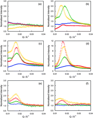 | ||
| Fig. 6 In-plane scans of the (a) native TA films, (b) RuO4 treated TA films, (c) native SEA films, (d) RuO4 treated SEA films, (e) native SEC films, and (f) RuO4 treated SEC films. The data for the f = 0.10 films (blue diamonds), 0.19 films (green triangles), 0.24 films (yellow circles), and 0.45 films (red squares) are shown. | ||
For the native films relatively strong scattering was observed from the SEA and SEC films. All of the observed peaks were relatively broad due to a combination of a moderately broad incident beam and a low level of ordering in the films. Nevertheless it can be seen in Table 3 that for the SEA films the spacing between scattering centres increases with increasing dPS content. The values are also consistent with those determined by FFT analysis of the AFM images, though scattering based figures are generally considered much more robust since they represent averages over a larger region of the sample.
| Film | Native | RuO4 treated | ||
|---|---|---|---|---|
| In-plane d/nm | AFM a period/nm | In-plane d/nm | AFM a period/nm | |
| a The periodicities were taken from FFT analysis of the AFM images. The bracketed numbers are the equivalent lattice parameters assuming that a hexagonal unit cell is present. | ||||
| TA-0.10 | — | — | — | — |
| TA-0.19 | — | 40 (35) | 34.3 | 42 (36) |
| TA-0.24 | — | 45 (39) | 39.6 | 51 (44) |
| TA-0.45 | — | 51 (44) | 36.1 | 50 (43) |
| SEA-0.10 | 30.3 | 33 (29) | 28.3 | 36 (31) |
| SEA-0.19 | 34.9 | 44 (38) | 34.3 | 51 (44) |
| SEA-0.24 | 36.8 | 48 (42) | 35.5 | 54 (47) |
| SEA-0.45 | 35.5 | 51 (44) | 37.4 | 51 (44) |
| SEC-0.10 | 36.8 | 42 (36) | — | 43 (37) |
| SEC-0.19 | 36.8 | 46 (40) | 44.7 | 54 (47) |
| SEC-0.24 | 38.8 | 50 (43) | 42.8 | 56 (49) |
| SEC-0.45 | 38.1 | 50 (43) | 38.8 | 53 (46) |
Similarly for the SEC films there was a correlation between the measured d-spacings and the dPS content, though this was weaker than in the SEA films. The SEC films also showed good agreement with the AFM results.
Strong scattering was observed for the SEA and SEC films as the contrast between adjacent structures is provided by the difference in the ED of the polymer film and vacuum rather than between the two polymers, which the XR results showed was not large. Subsequently the in-plane scans on the native TA films did not show any discernible scattering. For these films suitable contrast could only be obtained through the use of the RuO4 stain.
For the RuO4 treated TA films strong scattering was observed for both the TA-0.19 and TA-0.24 films, with weaker scattering from the TA-0.45 film. As the AFM images showed no significant changes between the pre- and post-RuO4 treated TA films, it can be concluded that the measured d-spacings for the RuO4 treated films correspond to the native films as well.
The lack of scattering from the TA-0.10 film is consistent with this film being in the uniform phase.
The most pronounced scattering from all of the samples was obtained with the RuO4 treated SEA samples, with the SEA-0.45 film displaying the first two peaks of a 2D hexagonal unit cell. For the SEA films it has been proposed that the dPS blocks form aggregates that are encased in a PMMA shell (Fig. 7).1,10 The scattering results reported here are broadly supportive of this hypothesis as the ruthenium stain will increase the ED of the dPS aggregates and thus increase the contrast between the polymer and vacuum.
 | ||
| Fig. 7 Schematics of structures of the SEA (top) and SEC (middle) films, and the SEC films after treatment with RuO4 (bottom). The dPS and PMMA domains are coloured grey and white respectively. | ||
Conversely, for the SEC films the addition of RuO4 leads to fewer and weaker peaks in the in-plane scans. For these films it was proposed that the PMMA formed a textured layer that was covered by a relatively homogenous layer of dPS (Fig. 7).1,10 The apparent loss of structure from these films cannot be attributed to large scale destruction of the order of the film as this is not supported by the AFM images. It is possible, however, to rationalise the changes by considering how the dPS portions of the film swell upon treatment with RuO4.
In considering the schematic of the SEC films shown in Fig. 7, it can be seen that the curvature of the overlying dPS layer depends on whether the dPS is on top of the PMMA ‘hills’ or located in the ‘valleys’ between the ‘hills’, a factor that will impact on the how the dPS layer expands upon reaction with RuO4. For a flat film, expansion occurs only normal to the surface, with the height change of the film being proportional to the volume change, however, the film thickness change becomes non-linear with volume change for curved surfaces. For a convex surface, such as that presented by the dPS portions on top of the PMMA ‘hills’, expansion of the film can occur both laterally and normal to the surface, subsequently the film thickness change (measured normal to the surface) will be smaller than the total volume change. For a concave surface, such as that present in the ‘valleys’, only expansion normal to the surface can occur; indeed, as adjacent parts of the dPS film will be trying to expand into the same space the thickness has to increase by more than the total volume to accommodate any expansion. It would therefore be expected that swelling of the dPS layer will give a thicker dPS layer in the ‘valleys’ than on the ‘hills’ leading to a smoothing-out of the surface (Fig. 7). As contrast in this system comes from the difference between the polymeric hills and the air surrounding them, the increased thickness of the dPS film in the ‘valleys’ will tend to reduce the overall contrast, leading to smaller scattering peaks.
The filling-in of the ‘valleys’ will also be dependent on the local curvature. For those areas with high curvature (i.e. where the spacing between adjacent PMMA ‘hills’ is small), the film thickness increase will be relatively larger. Coherent scattering from these features will subsequently be relatively less strong than from ‘hills’ spaced further apart, which will shift the scattering peak to lower Q values/higher d values, as was observed here (Table 3).
An unexpected result reported in Table 2 was the relatively high ruthenium content of the SEA films relative to the SEC and TA films. The reason for this is unknown, though it may be related to the packing of the dPS chains following forced precipitation from solution as opposed to the more equilibrium structures produced after thermal annealing or the evaporation of a good solvent. Alternatively the PMMA overlayer may influence the adsorption and reaction of RuO4.
Conclusions
Following on from previous work where we examined the microphase separation behaviour of several tethered dPS-b-PMMA films we report here the related X-ray scattering results.For films treated by thermal annealing contrast between the two blocks could only be achieved by reacting the film with a novel contrast enhancer. Due to the pseudo 2D nature of the phase separation within these films the staining procedure, while increasing the thickness of the dPS domains, did not significantly alter the lateral structure and periodicity of the films. Subsequently, the d-spacing measured for the RuO4 treated films is applicable to the native films as well. The stain also helped to confirm phase assignments previously made by AFM.
Normal to the surface the use of the stain confirmed that the dPS domains are located at the air/film interface in line with the expected behaviour.
The periodicities of films treated with a solvent exchange process were also measured. Though a stain was not required to get coherent scattering from these films it did enable the identification of higher order peaks in one of the samples.
Acknowledgements
The authors thank Dr Oier Bikondoa, ESRF, for his help with the synchrotron experiments; Drs Peter Harris and Chris Stain of the Centre for Advanced Microscopy, University of Reading, for their help with the RuO4 treatment and EDX results; and Prof. Joe Keddie, University of Surrey, for the use of his ellipsometer. This work was supported by EPSRC grant EP/F029616/1. Part of this work was performed on the EPSRC-funded XMaS beamline at the ESRF.References
- B. M. D. O'Driscoll, G. H. Griffiths, M. W. Matsen, S. Perrier, V. Ladmiral and I. W. Hamley, Macromolecules, 2010, 43, 8177–8184 CrossRef CAS.
- M. W. Matsen and G. H. Griffiths, Eur. Phys. J. E: Soft Matter Biol. Phys., 2009, 29, 219–227 Search PubMed.
- H. G. Haubruge, A. M. Jonas and R. Legras, Polymer, 2003, 44, 3229–3234 CrossRef CAS.
- S. M. Park, S. H. Yun and B. H. Sohn, Macromol. Chem. Phys., 2002, 203, 2069–2074 CrossRef CAS.
- R. W. Smith and V. Bryg, Rubber Chem. Technol., 2006, 79, 520–540 CAS.
- T. M. Chou, P. Prayoonthong, A. Aitouchen and M. Libera, Polymer, 2002, 43, 2085–2088 CrossRef CAS.
- S. M. Danauskas, D. Li, M. Meron, B. Lin and K. Y. C. Lee, Appl. Crystallogr., 2008, 41, 1187–1193 Search PubMed.
- Physical Properties of Polymers Handbook, ed. J. E. Mark, Springer, New York, NY, USA, 2nd edn, 2007 Search PubMed.
- Polymer Handbook, ed. J. Brandrup and E. H. Immergut, John Wiley & Sons, New York, NY, USA, 3rd edn, 1989 Search PubMed.
- B. Zhao, W. J. Brittain, W. Zhou and S. Z. D. Cheng, J. Am. Chem. Soc., 2000, 122, 2407–2408 CrossRef CAS.
Footnote |
| † Electronic supplementary information (ESI) available: AFM images of all of the samples discussed, full ellipsometric results and the XR profiles (with fits) for the TA films. See DOI: 10.1039/c0py00289e |
| This journal is © The Royal Society of Chemistry 2011 |