Significant enhancement of yellow–green light emission of ZnO nanorod arrays using Ag island films†
Chin-An
Lin
,
Dung-Sheng
Tsai
,
Cheng-Ying
Chen
and
Jr-Hau
He
*
Graduate Institute of Photonics and Optoelectronics, and Department of Electrical Engineering, National Taiwan University, Taipei, 10617, Taiwan (ROC). E-mail: jhhe@cc.ee.ntu.edu.tw; Fax: +886-2-2367-7467; Tel: +886-2-33669646
First published on 24th January 2011
Abstract
Surface plasmon (SP) mediated emission from ZnO nanorod arrays (NRAs)/Ag/Si structures has been investigated. The ratio of visible emission to UV emission can be increased by over 30 times via coupling with SP without deterioration of the crystal quality. The fact that the effect of SP crucially depends on the size of Ag island films provides the feasibility to significantly enhance the yellow–green emission of the ZnO nanostructures without sacrificing the crystallinity of ZnO.
1. Introduction
ZnO is regarded as a promising material with luminescence, electric conductivity, piezoelectricity and optical transparency.1 One-dimensional ZnO nanostructures2,3 have been extensively studied because of their potential applications in nanodevices such as gas sensors,4 light emitters,5,6 and field emitters.7,8 Many researchers have particularly investigated the luminescent properties of ZnO nanostructures, including near band edge (NBE) emission and deep level emissions.9–11 Moreover, most of the high quality ZnO NRAs have been synthesized by the high temperature methods such as metal organic chemical vapor deposition,12 a vapor–liquid–solid process,13 and thermal evaporation,14 which is difficult to control and energy consuming. The hydrothermal technique is an alternative method for synthesizing ZnO NRAs because of the low-temperature wafer-scale process.15Ag is well known for its strong interactions with visible light via the resonance of the oscillations of the electrons within the particles. These local electromagnetic fields near Ag can be many orders of magnitude higher than the incident fields, which include so-called surface plasmons (SPs). Generally SP-enhanced emission involves two sequential processes. Firstly, the excited energy in the emitter is transferred into SPs instead of photons. The resonant coupling of the excited states into SPs occurs when the energy of the excited states in the semiconductor approximates the SP energy of the metal layer.16 Secondly, SPs radiate light to far field if the momentum values match.16,17 In contrast, SPs are unable to generate photons directly while the momentum values of SPs and light do not match. Consequently, the SP energy trapped at the interface is dissipated as heat, leading the reduction of the luminescent efficiency.17 However, SP-mediated energy can be transferred by some methods. For example, as the grating structures with the periodicity or the interface corrugation are introduced appropriately, these SPs alter their momentum and thus couple to light, leading to the enhanced luminescent efficiency for light emission devices.16 Since metal-capped thin-film structures of emitters are usually adopted,18–21 it is difficult to investigate the influence of the interface roughness which is essential to enhance emission. To our knowledge, the effect of interface corrugation on the luminescent enhancement of ZnO nanostructures has not yet been investigated.
In this study, based on the ZnO NRAs/Ag/Si structure using a low-temperature hydrothermal method, the investigation on the effect of interface morphology on the enhancement of SP-mediated emission becomes possible without altering the crystal quality. The ratio of visible emission to UV emission can be increased by over 30 times via coupling with SPs. To examine crystal quality and chemical information of the surface of ZnO NRAs, X-ray diffraction (XRD) and X-ray photoelectron spectroscopy (XPS) have been performed. The use of SPs paves the way for further development of the ZnO NRA-based light emitting devices.
2. Experimental details
Synthesis
The growth of ZnO NRAs was carried out using a hydrothermal process. We prepared the silicon (100) substrate coated with 5, 10 and 30 nm thick Ag films by e-beam evaporation. The Ag island films on the Si substrates can be obtained after annealing at 300 °C in air for 25 min. A thin film of zinc acetate was spin-coated on the bare Si and Ag/Si substrates with the ethanol solution containing 5 mM zinc acetate dihydrate. 5 nm thick ZnO films as the seed layers were obtained after annealing samples at 300 °C in air for 25 min. ZnO NRAs were grown in aqueous solution containing zinc nitrate hexahydrate (10 mM) and ammonia solution at 95 °C for 2 h. The synthesized products were cleaned with ethanol to remove impurities and then dried in an air ambient.Characterization
After the growth process, the resulting products were collected for phase identification using XRD with a fixed incident angle of 0.5°. Morphological study of ZnO nanostructures has been performed with a JEOL JSM-6500 field emission scanning electron microscopy (SEM). The photoluminescence (PL) measurements were performed using a He–Cd laser at room temperature. The electronic structures of NRAs were confirmed by PHI Quantera XPS. XPS is a widely used technique for obtaining chemical nature from the material surfaces (3–5 nm in depth). In this study, Ar sputtering was performed to etch ZnO NRA surfaces in the XPS system before the electronic structures of NRAs was evaluated using XPS. The absorption spectra were measured with a JASCO V-670 UV-visible spectrometer in the spectral ranges from 400 to 800 nm.3. Results and discussion
The hydrothermal method is adapted in the present study since it is easy to grow ZnO nanorods perpendicularly to the surface of arbitrary substrates regardless of their lattice match or surface chemistry.15,22 Before ZnO NRAs were grown from the textured ZnO seeds in aqueous solution at 95 °C for 2 h, several thicknesses of Ag with identical thermal treatment were chosen to prepare suitable Ag nanostructures on the Si substrates for coupling with the ZnO NRAs. The surface morphologies of Ag island films with different thicknesses (i.e., 5, 10 and 30 nm) on the Si substrates after annealing at 300 °C for 25 min are shown in the insets of Fig. 1(b)–1(d). Compared to the unannealed Ag island films/Si substrates (as shown in Fig. S1†), the surface morphology of Ag island films was varied by the annealing. As the thickness of Ag thin film is increased, the size of Ag island structures is expected to become larger with more irregular shape. It has been known that the size and shape of metal islands determine the resonance energy of a generated SP. The surface morphologies of the ZnO NRAs grown directly on bare Si substrates and Si substrates with different thickness of Ag island films are shown in Fig. 1(a)–1(d). Note that the growth conditions of ZnO NRAs are identical in all samples. The sample without Ag island films composed of ZnO NRAs shows perfect perpendicular alignment to the substrate surface, as indicated in Fig. 1(a). One can see that the Ag island films indeed increase the diameter of the ZnO NRAs although the thickness of Ag island films does not vary with the diameter of ZnO NRAs significantly. The diameters of ZnO NRAs on bare Si (∼61.6 nm) are much smaller than that on Ag/Si (∼110 nm). This is because the heterogeneous nucleation for ZnO NRA growth on Ag/Si substrates can be much easier since stable nucleus is already present with the aid of Ag island films as compared to the ZnO NRA growth on Si substrates. It is observed that the degree of vertical alignment of the ZnO NRAs decreased slightly due to the increased roughness of the surface with the thickness of Ag island films, as shown in Fig. 1(b)–1(d).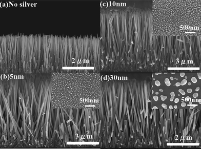 | ||
| Fig. 1 The cross-sectional SEM images of ZnO NRAs grown on Ag/Si substrates with various thicknesses of Ag island films. The insets are the corresponding morphologies of Ag island films on Si substrates after annealing at 300 °C in air for 25 min. | ||
The structure of the as-synthesized NRAs was determined by XRD analysis. Fig. 2 shows the XRD pattern of the as-grown NRAs. A strong peak locates at 34.52° for the diffraction from (002) plane of ZnO. The recognizable peaks at 31.78°, 36.32°, 47.72° and 63.96° refer to the (100), (101), (102) and (103) planes of ZnO, respectively. All of the diffraction peaks for all samples can be ascribed to the wurtzite ZnO structure with lattice constants of a = 0.3249 nm and c = 0.5205 nm, consistent with the standard data file (JCPDS 05-0664). It can be inferred that all ZnO NRAs were preferentially oriented in the c-axis direction.
 | ||
| Fig. 2 The XRD patterns of ZnO NRAs grown on Ag/Si substrates with the various thicknesses of the Ag films. | ||
As the substrate has a high refractive index and/or high absorption coefficient, the information contained in the extinction spectrum can be quite poor. We use the fused silica as the substrate instead of the silicon. The absorption spectra allow the observation and characterization of the excited SP resonance modes.23Fig. 3 shows the UV-visible absorption spectra of various Ag island films/fused silica substrates with and without 5 nm thick ZnO seed layers after annealing samples at 300 °C in air for 25 min. Larger Ag islands lead to the redshift of the absorptance maximum with increasing intensity. The broad absorption spectra are due to the irregular size of the Ag islands. In addition, it has been previously described that the optical properties of Ag nanoparticles depend on the external dielectric constant.24–26 By taking into account of the difference of dielectric constants between ZnO and air, one can see that different resonance frequencies between ZnO/Ag and air/Ag are obtained, i.e., the resonance frequency redshifts as the dielectric constant of the surrounding medium is increased, as shown in Fig. 3. Ag islands act as radiative antenna coupling SP into light emission.27 Generally, smaller Ag islands lead to higher SP resonance energies. As the size of Ag islands is increased with the large variation in the surface roughness, the redshift of the absorbance maximum and large inhomogeneous broadening are observed.28,29 Similar results were also investigated experimentally and theoretically in the Ag/ZnO nanocomposite films.23
 | ||
| Fig. 3 The absorption spectra of Ag island films/fused silica substrates, and the 5 nm thick ZnO films/Ag island films/fused silica after annealing at 300 °C in air for 25 min. | ||
Fig. 4 shows a comparison of PL spectra of ZnO NRAs on 5, 10, and 30 nm thick Ag island film/Si and bare Si substrates. A control sample only consisting of ZnO NRAs on the Si substrate shows a typical PL spectrum of ZnO with a strong NBE emission at 382 nm and weak yellow–green emission at 568 nm from the deep levels related to a complex of an oxygen vacancy and zinc interstitial.9,30 Note that the peak at 760 nm results from the second-order feature of the NBE emission of ZnO. One can see that the yellow–green emission increases greatly with the thickness of the Ag island films. It has been reported that the intensity of deep level emission was enhanced while the diameter of nanowires was decreased (i.e., surface area was increased).31 In our study, however, large-diameter ZnO NRAs with the aid of the Ag films show a significant enhancement of the deep level emission, which is different from previous reports.31 We can exclude the possibility that the giant enhanced yellow–green emission is caused by the density of deep level traps. The ratio of visible emission to UV emission of ZnO NRAs with the thickness of Ag island films is listed in Table 1.
 | ||
| Fig. 4 The PL spectra of ZnO NRAs on bare Si substrate and Ag/Si substrates with the various thicknesses of the Ag films. | ||
| Thickness of Ag films (nm) | Ratio of visible emission to UV emission |
|---|---|
| 0 | 0.32 |
| 5 | 1.72 |
| 10 | 5.35 |
| 30 | 10.11 |
It has been known that the recombination of deep levels responsible for visible emission in ZnO nanostructures is located at the surface (<30 nm in thickness).31 To judge if the enhancement of yellow–green emission is related with the deteriorated crystal quality, the results of XRD and XPS were investigated. Fig. 2 presents the XRD pattern of the ZnO NRAs grown on a Ag/Si substrate. Stronger ZnO (002) peak was observed in all Ag/Si substrates than that on bare Si substrates, which demonstrated that the crystal quality of the ZnO NRAs was somewhat improved when it was deposited on an Ag interlayer. XPS, also known as electron spectroscopy for chemical analysis, is a widely used technique for obtaining chemical nature from the material surfaces (3–5 nm in depth) with the detection limit of 1 at.%. Fig. 5 shows the O 1s and the Zn 2p3 core level spectra of ZnO NRAs on Ag island films/Si and bare Si substrates. The binding energy of the O 1s and Zn 2p3 were recorded to be 530.8 eV and 1022.2 eV, respectively. Since the number of photoelectrons of an element depends on the atomic concentration of that element in the samples, XPS is used to not only identify the elements but also quantify the chemical composition. Moreover, the XPS measurements have been carried out to investigate the chemical states of the O 1s and Zn 2p3 in the ZnO.32–35 O 1s of ZnO NRAs can be deconvoluted by three nearly Gaussian curves, centered at 530.1, 530.8, and 531.9 eV in all samples. An example is O 1s of ZnO NRAs without Ag island films as shown in Fig. S2.† The high binding energy component located at 531.9 eV is usually attributed to chemically absorbed oxygen on the surface of the ZnO NRAs. The component near 530.1 eV is attributed to O2− ions surrounded by Zn atoms with their full complement of nearest-neighbor O2− ions. The intensity of this component is related to the amount of oxygen atoms in a fully oxidized stoichiometric surrounding. The binding energy component, centered at 530.8 eV, is associated with the amount of O2− ions in the oxygen deficient regions within ZnO NRAs. Therefore, the change in ratio of intensities of three components can be connected to the variations in the concentration of oxygen deficiencies. In the present study, the quite similar shape of O 1s leads to an invariable ratio of intensities of three components in all samples, indicating that the concentration of oxygen deficiencies was not varied with the thickness of Ag island films. After the value of peak intensity (the peak area after background removal) is obtained, the atomic concentration of an element (Ci) can be expressed as:
 | (1) |
 | ||
| Fig. 5 The XPS spectra of (a) O 1s and (b) Zn 2p3 core levels of ZnO NRAs on Ag/Si substrates with the various thicknesses of the Ag films. | ||
| Thickness of Ag films (nm) | Atomic concentration of oxygen (%) | Atomic concentration of zinc (%) |
|---|---|---|
| 0 | 46.01 | 53.99 |
| 5 | 47.40 | 52.60 |
| 10 | 47.60 | 52.40 |
| 30 | 47.86 | 52.14 |
It has been found that scattering cross section of the SP increases with the square of metal island volume.36 With the increase of the Ag island size, the scattering efficiency of the SPs is raised. Thus, we attribute this enhancement to SP-mediated emission, in which the deep level emission within ZnO NRAs couples into the SP modes at the Ag/ZnO interface when the excited energy and the SP energy are similar. Then, the spontaneous recombination produces SPs instead of photons. The coupled SP energy can be recovered as free space photons when the interface is rough appropriately to scatter the photons. The ratio of visible emission to UV emission can be increased by over 30 times via coupling with SPs. Moreover, the decrease of UV emission with the increasing thickness of Ag island films was observed. It can be attributed to the enhanced recombination rate of the deep level emission due to the coupling of the emission with SPs at the Ag-ZnO surface. The recombination rate is enhanced through the ZnO-SP coupling rate, which is expected to be very fast compared to the radiative and nonradiative recombination rates.37 Thus, the UV emission is quenched while the visible emission is enhanced. In addition, this difference of enhanced ratio of visible emission to UV emission disproves the possible attribution of the stronger PL intensity of ZnO NRAs to the metal reflection.
4. Conclusions
In summary, depositing ZnO NRAs on a metal layer using a hydrothermal method provides a convenient approach to investigate the effect of corrugated Ag films on SP-enhanced emission. The experimental results show that the deep level emission of ZnO NRAs was strongly enhanced by SP resonant coupling instead of deteriorated crystal quality. It was found that Ag islands of large size with high scattering efficiency lead to strong enhancement of PL. This gives a promising way for modulating light intensity at the nanoscale via coupling through SP of metal islands.Acknowledgements
The research was supported by the National Science Council 99-2120-M-007-011, 99-2112-M-002-024-MY3, 99-2622-E-002-019-CC3 and Aim for Top University Project from the Ministry of Education.References
- U. Ozgur, Y. I. Alivov, C. Liu, A. Teke, M. A. Reshchikov, S. Dogan, V. Avrutin, S. J. Cho and H. Morkoc, J. Appl. Phys., 2005, 98, 041301 CrossRef.
- Z. L. Wang, J. Phys.: Condens. Matter, 2004, 16, R829 CrossRef CAS.
- X. Fang, L. Hu, C. Ye and L. Zhang, Pure Appl. Chem., 2010, 82, 2185 CrossRef.
- J. H. He, Y. H. Lin, M. E. McConney, V. V. Tsukruk, Z. L. Wang and G. Bao, J. Appl. Phys., 2007, 102, 084303 CrossRef.
- J. H. He, J. H. Hsu, C. W. Wang, H. N. Lin, L. J. Chen and Z. L. Wang, J. Phys. Chem. B, 2006, 110, 50 CrossRef CAS.
- X. Fang, Y. Bando, U. K. Gautam, T. Zhai, H. Zeng, X. Xu, M. Liao and D. Golberg, Crit. Rev. Solid State Mat. Sci., 2009, 34, 190 Search PubMed.
- X. D. Bai, E. G. Wang, P. X. Gao and Z. L. Wang, Nano Lett., 2003, 3, 1147 CrossRef CAS.
- X. Fang, Y. Bando, U. K. Gautam, C. Ye and D. Golberg, J. Mater. Chem., 2008, 18, 509 RSC.
- A. B. Djurisic and Y. H. Leung, Small, 2006, 2, 944 CrossRef CAS.
- C. W. Wang, J. H. He and L. J. Chen, Mater. Sci. Technol., 2008, 24, 633 CrossRef CAS.
- C. Y. Chen, M. W. Chen, J. J. Ke, C. A. Lin, J. R. D. Retamal and J. H. He, Pure Appl. Chem., 2010, 82, 2055 CrossRef.
- J. Zhong, S. Muthukumar, Y. Chen, Y. Lu, H. M. Ng, W. Jiang and E. L. Garfunkel, Appl. Phys. Lett., 2003, 83, 3401 CrossRef CAS.
- J. H. He, C. H. Ho, C. W. Wang, Y. Ding, L. J. Chen and Z. L. Wang, Crystal Growth & Design., 2009, 9, 17 CrossRef CAS.
- R. C. Wang, C. P. Liu, J. L. Huang and S. J. Chen, Appl. Phys. Lett., 2005, 86, 251104 CrossRef.
- L. Guo, Y. L. Ji, H. B. Xu, P. Simon and Z. Y. Wu, J. Am. Chem. Soc., 2002, 124, 14864 CrossRef CAS.
- K. Okamoto, I. Niki, A. Shvartser, Y. Narukawa, T. Mukai and A. Scherer, Nat. Mater., 2004, 3, 601 CrossRef CAS.
- W. L. Barnes, Nat. Mater., 2004, 3, 588 CrossRef CAS.
- J. B. You, X. W. Zhang, Y. M. Fan, Z. G. Yin, P. F. Cai and N. F. Chen, J. Phys. D: Appl. Phys., 2008, 41, 205101 CrossRef.
- A. P. Abiyasa, S. F. Yu, S. P. Lau, E. S. P. Leong and H. Y. Yang, Appl. Phys. Lett., 2007, 90, 205101.
- J. Li and H. C. Ong, Appl. Phys. Lett., 2008, 92, 121107 CrossRef.
- P. H. Cheng, D. S. Li, Z. Z. Yuan, P. L. Chen and D. R. Yang, Appl. Phys. Lett., 2008, 92, 041119 CrossRef.
- L. E. Greene, M. Law, D. H. Tan, M. Montano, J. Goldberger, G. Somorjai and P. D. Yang, Nano Lett., 2005, 5, 1231 CrossRef CAS.
- R. K. Roy, S. Bandyopadhyaya and A. K. Pal, Eur. Phys. J. B, 2004, 39, 491 CrossRef CAS.
- T. R. Jensen, M. L. Duval, K. L. Kelly, A. A. Lazarides, G. C. Schatz and R. P. Van Duyne, J. Phys. Chem. B, 1999, 103, 9846 CrossRef CAS.
- T. R. Jensen, M. D. Malinsky, C. L. Haynes and R. P. Van Duyne, J. Phys. Chem. B, 2000, 104, 10549 CrossRef CAS.
- C. Bohren and D. Huffman, Absorption and Scattering of Light by Small Particles, Wiley, New York ( 1983) Search PubMed.
- I. Gontijo, M. Boroditsky, E. Yablonovitch, S. Keller, U. K. Mishra and S. P. DenBaars, Phys. Rev. B: Condens. Matter, 1999, 60, 11564 CrossRef CAS.
- J. R. Lakowicz, Anal. Biochem., 2005, 337, 171 CrossRef CAS.
- R. Gans, Ann. Phys., 1912, 342, 881 CrossRef.
- P. S. Xu, Y. M. Sun, C. S. Shi, F. Q. Xu and H. B. Pan, Nucl. Instrum. Methods Phys. Res., Sect. B, 2003, 199, 286 CrossRef CAS.
- I. Shalish, H. Temkin and V. Narayanamurti, Phys. Rev. B: Condens. Matter Mater. Phys., 2004, 69, 245401 CrossRef.
- S. Baek, J. Song and S. Lim, Phys. B, 2007, 399, 101 CrossRef CAS.
- M. Chen, X. Wang, Y. H. Yu, Z. L. Pei, X. D. Bai, C. Sun, R. F. Huang and L. S. Wen, Appl. Surf. Sci., 2000, 158, 134 CrossRef CAS.
- J. C. C. Fan and J. B. Goodenough, J. Appl. Phys., 1977, 48, 3524 CrossRef CAS.
- J. Song, S. Baek and S. Lim, Phys. B, 2008, 403, 1960 CrossRef CAS.
- U. Kreibig and M. Vollmer, Optical Properties of Metal Clusters, Chapter 2, Springer, Berlin ( 1995) Search PubMed.
- C. K. Choi, Y. H. Kwon, B. D. Little, G. H. Gainer, J. J. Song, Y. C. Chang, S. Keller, U. K. Mishra and S. P. DenBaars, Phys. Rev. B: Condens. Matter, 2001, 64, 245339 CrossRef.
Footnote |
| † Electronic supplementary information (ESI) available. See DOI: 10.1039/c0nr00732c |
| This journal is © The Royal Society of Chemistry 2011 |