Thickness dependent self limiting 1-D tin oxide nanowire arrays by nanosecond pulsed laser irradiation
N.
Shirato
a,
J.
Strader
bc,
A.
Kumar
d,
A.
Vincent
d,
P.
Zhang
d,
A.
Karakoti
e,
P.
Nacchimuthu
e,
H.-J.
Cho
d,
S.
Seal
dfg and
R.
Kalyanaraman
*abc
aDepartment of Materials Science and Engineering, University of Tennessee, Knoxville, TN 37996, USA. E-mail: ramki@utk.edu
bSustainable Energy Education and Research Center (SEERC), University of Tennessee, Knoxville, TN 37996, USA
cDepartment of Chemical and Biomolecular Engineering, University of Tennessee, Knoxville, TN 37996, USA
dDepartment of Mechanical, Materials and Aerospace Engineering, University of Central Florida, FL 32816, USA
eEnvironmental Molecular Sciences Laboratory, Pacific Northwest National Lab, Richland, WA 99352, USA
fAdvanced Materials Processing Analysis Center, University of Central Florida, FL 32816, USA
gNanoscience Technology Center, University of Central Florida, FL 32816, USA
First published on 23rd December 2010
Abstract
Fast, sensitive and discriminating detection of hydrogen at room temperature is crucial for storage, transportation, and distribution of hydrogen as an energy source. One dimensional nanowires of SnO2 are potential candidates for improved H2 sensor performance. The single directional conducting continuous nanowires can decrease electrical noise, and their large active surface area could improve the response and recovery time of the sensor. In this work we discuss synthesis and characterization of nanowire arrays made using nanosecond ultraviolet wavelength (266 nm) laser interference processing of ultrathin SnO2 films on SiO2 substrates. The laser energy was chosen to be above the melting point of the films. The results show that the final nanowire formation is dominated by preferential evaporation as compared to thermocapillary flow. The nanowire height (and hence wire aspect ratio) increased with increasing initial film thickness h0 and with increasing laser energy density Eo. Furthermore, a self-limiting effect was observed where-in the wire formation ceased at a specific final remaining thickness of SnO2 that was almost independent of h0 for a given Eo. To understand these effects, finite element modeling of the nanoscale laser heating was performed. This showed that the temperature rise under laser heating was a strong non-monotonic function of film thickness. As a result, the preferential evaporation rate varies as wire formation occurs, eventually leading to a shut-off of evaporation at a characteristic thickness. This results in the stoppage of wire formation. This combination of nanosecond pulsed laser experiments and thermal modeling shows that several unique synthesis approaches can be utilized to control the nanowire characteristics.
1. Introduction
As the use of hydrogen (H2) gas as an alternative clean energy source is stimulated, accurate and fast detection of the H2 will become exceedingly important for its safe handling, transportation and operation. Vehicles utilizing domestic fuel cell based cogeneration systems,1 solid oxide fuel cell (SOFC) technology,2 and internal combustion engines3 are already commercialized H2 powered systems. Due to its very small size, H2 is very susceptible to leakage. Since H2 molecules are quite reactive in the vapor phase, typically about 1–3 vol % of H2 is considered to be explosive, hence, careless treatment can lead to expensive and damaging incidents. Thus, precise control of the gas is essential, especially viadetection of leaks. Currently, there are several available techniques for measuring H2 gas concentration, including conductivity changes in pure continuous or porous SnO2 films4–6 and in TiO2 nanotubes arrays,7,8 measurement of surface plasmon resonance utilizing palladium,9 using the Schottky effect in Pt-Carbide10 and carbon nanotubes decorated with Pd nanoparticles. However, there are several challenging issues that remain to be solved, such as the requirements of low working temperature (room temperature and below), fast response and recovery time, as well as high sensitivity and selectivity.SnO2 thin films have been of interest for several applications such as transistors, electrode materials, and solar cells and are also known for its excellent gas sensitivity.11SnO2 doped with various appropriate elements, such as In2O3,12CuO13 and Pd,14 is a promising area of research for improved gas sensor performance. This type of doping generates an excess concentration of lattice oxygen-ion vacancies and decreases the concentration of free electrons to maintain the charge balance. In addition, the size and morphology of SnO2 grains and nanostructures15 strongly affects their application and therefore appropriately doped and nanostructured SnO2 can serve as ultrasensitive gas sensors.16 In this paper, we explore the synthesis of arrays of one dimensional (1-D) nanowires of SnO2, with the eventual goal of fabricating In2O3-doped SnO2, which is a potential candidate for improved H2 sensors. The doped In3+ cations are effective in increasing the number of active surface area sites enabling the sensor to detect H2 at lower operating temperatures.
A primary motivation to explore the synthesis of well-defined nanostructures is the associated increase in surface-to-volume ratio, which is known to translate into increased sensitivity, selectivity, and response speed of the H2 sensor.17 Another potential advantage of an array of continuous nanowires is a decrease in the electrical noise, as compared to, for example, a porous type nanostructure.18 Here we focus on synthesis and characterization of arrays made from thin films of pure SnO2 on SiO2 substrates by use of nanosecond pulses of ultraviolet (UV) wavelength (266 nm) laser. Pulsed laser interference irradiation is a well-known means of creating a well-defined and spatially periodic but transient surface temperature profile.19–21 For appropriate energy densities, the film can be locally evaporated or melted, with the liquid being subject to strong thermocapillary forces under the thermal gradients. As a result, a periodic structuring of the film material can take place. For irradiation with nanosecond pulses, the heating and cooling rates are extremely large22–24 and as a result, the morphology changes occurring in the liquid phase can be rapidly quenched, resulting in periodic structures.25 However, as has been shown recently, nanoscale effects strongly influence the UV laser heating of very thin films, often resulting in unusual and unexpected effects on morphology evolution.26,27 Here we have utilized a thermal model based on finite element analysis that accurately accounts for the nanoscale thickness dependent optical and thermal behavior of the film-substrate system in order to predict the thermal behavior of the films. By comparison with experimental observations of melting and array formation, a reliable model for the mechanism of nanowire array formation was established. We also observed experimentally that the final effective thickness of SnO2 remaining after array formation was nearly constant for various starting film thickness at a given laser energy density. This self-limiting effect was due to the strong thickness-dependent temperature of the film under laser irradiation for any given energy density. As a result, thermal evaporation and thermocapillary flow can both shut down as the film morphology evolves. Other features of the nanowire morphology, including nanowire height and aspect ratio were found to increase with increasing film thickness and laser energy. These results are qualitatively consistent with the thermal model result based on the temperature difference between the regions of interference maxima and minima. The experimental and supporting theoretical modeling results permits selection of the appropriate thin film and laser parameters to achieve desired nanowire morphology characteristics.
2. Experimental details
Thin films of SnO2, with thickness between 5 to 100 nm, were deposited onto 400 nm thick thermally grown SiO2 on Si wafers and quartz wafers by pulsed laser deposition (PLD). The substrates were ultrasonically rinsed and dried in air prior to use. Deposition was performed under ultrahigh vacuum (UHV) conditions, at a base pressure of 10−7 Torr, with the substrate at room temperature. SnO2 slugs (99.9% purity, obtained from CERAC, inc.) were used as PLD targets. Thickness of the as-deposited films was measured by performing atomic force microscopy (AFM) on a step-height region generated by the application and subsequent removal by acetone of a nitrocellulose mask. AFM analysis also yielded a maximum root mean square (RMS) roughness of the as-deposited films of 0.3 nm. Energy dispersive X-ray spectroscopy (EDS) measurements were employed to determine the relative concentration of Sn within the electron interaction zone. The resulting concentrations were then fitted on a power-law curve, so that subsequent measurements of the effective thickness of the laser irradiated films could be determined from the EDS measurements. The optical properties of the as-deposited films were measured by an Ocean Optics HR2000+ spectrometer in order to obtain the accurate complex refractive index values for the deposited films, which are known to differ from bulk values.28Laser processing was performed with the 4th harmonic (266 nm wavelength) of an Nd:YAG laser, with a 9 ns pulse width and a repetition rate f = 50 Hz. All the results presented here are based on irradiations done under ambient conditions. First, the melt threshold energy for various SnO2 film thickness (5 and 42 nm) was obtained by normal incidence single beam irradiation with 3000 pulses at various laser energy densities, Eo. The melt threshold was defined as the minimum energy required to show a substantial morphology change to the surface of the film after substantial irradiation times, as has been done in the past.23 This morphology change was evidenced in a scanning electron microscope (SEM). These measurements enabled a quantitative comparison of the experimentally determined melting energy with the finite element model for laser heating of the films. Based on the melt threshold energies determined by single beam experiments, two-beam laser irradiation was performed for nanowire array synthesis. The laser beam was split into two equal energy beams using a 50–50 beam splitter and were incident on the sample at inclusive angle, θi, of 72° (and 86°) with a resulting theoretical interference fringe spacing of 224 nm (and 195 nm) respectively. Approximately 3000 pulses were applied in order to produce an array of wire-like features within the irradiated area. The resulting film morphology was characterized by SEM (using either a Hitachi S4300N or a Gemini: LEO 1525), AFM in a Nanonics MultiView 1000, and by EDS measurements in the LEO 1525. The elemental compositions of select samples were also characterized by X-ray photoelectron spectroscopy (XPS) using a Physical Electronics (PHI5400 ESCA) spectrometer with a monochromatic Al KαX-ray source operated at 300W. The crystal structures of as-deposited and select nanowire samples were characterized by X-ray diffractometry (XRD) using a Rigaku D/MAX RAPID II microdiffractometer with a curved imaging plate and a rotating Cr anode operating at 35 kV and 25 mA. An optical prefix consisting of horizontal and vertical mirrors specific to Cr Kα radiation was employed in the incident beam to provide a focused X-rays at the sample position. At the end of the incident beam path, a 0.3 mm collimator was used to optimize the resolution and signal to noise ratio of the diffraction patterns. The incident beam path from X-ray generator to the collimator was protected by o-ring sealed tubing that was purged with Helium gas to improve the X-ray flux at the sample position. The samples were mounted on a stainless steel sample holder with the X-ray beam 2° off axis from the plane of the sample.
3. Results
3.1. Experimental results
Fig. 1 (a) shows the SEM image of an SnO2 nanowire array synthesized from SnO2 films of initial thickness ho = 42 nm and at an energy density of 300 mJ cm−2 with θi = 72°. This and similar SEM micrographs were used to analyze the average spacing Λav of the nanowires in the array. Also, EDS measurements performed over large portions of the array, ∼100μm, were used to estimate the remaining amount (hrem) of SnO2 in the array. Fig. 1 (b) shows the AFM image of the same sample for which the SEM image is shown in Fig. 1 (a). AFM was performed to extract the topographic information of the wires, from which line profiles, such as shown in Fig. 1 (c), were extracted. From such line profiles, the average nanowire height hnw was measured as the value between the peak to trough of the nanowires averaged over large portions of the array. The surface elemental composition of the SnO2 before and after laser processing was evaluated using XPS. In Fig. 2, XPS spectra of Sn 3d5/2 measured on the as-deposited SnO2 film of thickness 42 nm and nanowires synthesized at a laser energy density of 300 mJ cm−2 from the 42 nm film are shown. The photoemission intensity peaks occur at 486.46 and 486.57 (eV) respectively, for the two surfaces, and this corresponds well to the Sn4+ binding energy component of stoichiometric SnO2, which is at 486.3 eV.29 The Sn 3d5/2 peak for SnO is 0.5 eV lower than the SnO2 peak and we did not observe this peak shift in the nanowires sample. This suggests that upon irradiation of the as-deposited SnO2 films, the formation of nanowires is not assisted by valence change, and thus the nanowires remained as SnO2.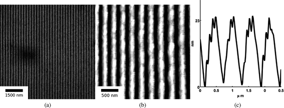 | ||
| Fig. 1 (a) SEM images of SnO2 nanowires synthesized from a 42 nm film at 300 mJ cm−2 and an interference angle of 72°. SnO2 rich and poor regions correspond to bright and dark contrasts, respectively. The average nanowire spacing is 232.3 nm while average width was estimated to be 97 nm. (b) AFM topography image of SnO2 nanowires of the same sample as (a). (c) A typical AFM line profile of the nanowires of (b). From such line profiles, the average nanowire height, hnw, could be calculated, and in this case it was 16 nm. | ||
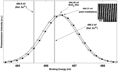 | ||
| Fig. 2 XPS (X-ray photoelectron spectroscopy) spectra of Sn 3d5/2 measured on SnO2 film and nanowires. The film (line with open symbols) and nanowires (line with closed symbols) photoemission intensity peaks of, 486.46 and 486.57 (eV) respectively, correspond with the binding energy of Sn4+ component, which is 486.3 (eV).29 Inset shows SEM image of nanowire region from which XPS was measured. | ||
The crystal structure of the samples before and after the irradiation was evaluated by glancing angle XRD. JADE 8.5 from Materials Data Inc., and PDF4+ database from ICSD were used to analyze X-ray diffraction data. Fig. 3 (a) and (b) shows the background subtracted XRD data of the nanowires synthesized from an as-deposited 42 nm film and following synthesis of nanowires with laser energy of 535 mJ cm−2 and interference angle of 86°, respectively. Analysis of the nanowire sample indicated a polycrystalline tetragonal crystal structure with lattice parameters of a = 4.78 Å and c = 3.21 Å, but the initial SnO2 film was found to be highly oriented, with only the (110) and (220) peaks of SnO2 appearing in the XRD scans. No change in the lattice parameter was found between the two samples.
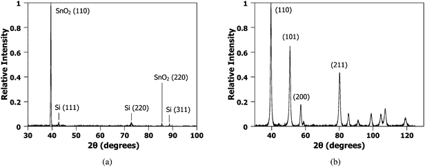 | ||
| Fig. 3 Glancing angle XRD data from SnO2 film and nanowires. (a) XRD of the as-deposited SnO2 film of 42 nm thickness. The film is highly oriented showing primarily the (110) and (220) reflections with a tetragonal structure. (b) XRD from nanowires synthesized from the 42 nm film with laser energy of 535 mJ cm−2 and interference angle of 86°. Here, the SnO2 is polycrystalline but with the same tetragonal structure with lattice parameters of a = 4.78 Å and c = 3.21 Å. | ||
The quality of nanowires, or equivalently, its quantitative morphological characteristics given by hnw, hrem, and the aspect ratio given by AR = hnw Λ−1av (where Λ−1av is the average spacing), was next investigated as a function of initial film thickness ho for various laser energy densities Eo. In Fig. 4, SEM images of the nanowires formed from two different ho values but from similar Eo (308 mJ cm−2), interference angle (72°) and number of pulses (3000) are shown. A clear difference in morphology can be seen between the two arrays with films of larger ho producing a more well defined nanowire structure. In Fig. 5, the AFM measurements and typical line scans of the wire profile for three different ho values prepared with above energy and interference conditions are shown. The average nanowire height, hnw, was obtained by averaging over 128 consecutive line scans, corresponding to a length of 375 nm, over 7 nanowires. The hrem value was measured using EDS over an area of 100 μm2 (or approximately 50 wires) at a location corresponding to the AFM measurements. The results of these measurements are shown in Fig. 6 for the various thicknesses. Fig. 6 (a) corresponds to the average hnw (open symbols correspond to experimental measurements) while Fig. 6 (b) is the remaining film thickness hrem. Fig. 6 (a) clearly shows that hnw, and therefore the aspect ratio of the wire increases with increasing initial film thickness ho. This behavior is especially important from viewpoint of maximizing the effective surface area for use in sensor applications. On the other hand, Fig. 6 (b) shows that the final amount hrem of SnO2 is 14 ± 1 nm, which is substantially lower then the starting thickness. This clearly points to a large contribution from evaporation for the wire synthesis. More interesting however, is the little dependence of hrem on the initial thickness ho for processing at a constant laser energy density Eo. Nanowires derived from films that undergo substantial evaporation (ho ≫ hrem), such as Fig. 5 (b) and (c), yield a continuous nanowire structure, but samples produced where evaporation was negligible (ho ≈ hrem), Fig. 4 (b), show nanoparticles in contact with each other. One important observation on the synthesis of nanowires is its dependence on the number of laser pulses. While the dependence on film thickness (and energy, which is discussed next) was performed at a fixed number of pulses (3000), the actual final state of the wires is typically formed at a much shorter number of pulses. In other words, the wire formation appears to stop very early in the irradiation and further irradiation does not result in any changes to the wire characteristics. Therefore, following 3000 pulses the morphology is in a stable state and does not progress further. This observation points to a self-limiting or self-stopping mechanism, where the wire formation ceases due to intrinsic conditions.
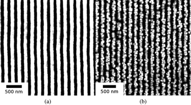 | ||
| Fig. 4 SEM images of SnO2 nanowires formed from two different initial film thickness (a) ho = 90 nm and (b) ho = 15 nm using the same interference angle, θi = 72° and 3000 pulses at an energy density of 308 mJ cm−2. The average nanowire spacing of (a) and (b) are 221 nm and 216 nm respectively. | ||
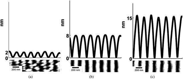 | ||
| Fig. 5 AFM topography image and line scans of the wire profile of SnO2 nanowire arrays formed from three different initial film thickness, (a) ho = 15, (b) ho = 25 and (c) ho = 90 nm respectively. The SEM images of the samples ho = 15 and 90 nm are shown in Fig. 4. All three nanowires were synthesized using the same interference angle, θi = 72° and 3000 pulses at an energy density of 308 mJ cm−2. The average nanowire height of each sample is (a) hnw = 2, (b) hnw = 8 and (c) hnw = 15 nm. | ||
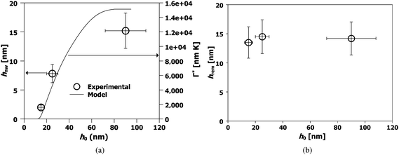 | ||
| Fig. 6 Behavior of the nanowire characteristics prepared at the same laser energy density as a function of starting film thickness. (a) Experimentally determined nanowire height hnw (open circles, left axes) and theoretically estimated integrated evaporation Γ* (line, right axes). The nanowire height hnw increases with increasing starting film thickness ho. (b) Observation of the self-limiting effect. The experimentally measured remaining film thickness hrem (symbols) is almost similar for all the films. The laser energy density used was 300 mJ cm−2, the interference angle was 72° and the number of pulses was 3000 for all samples. | ||
Next, we investigated the dependence of nanowire morphology on the laser energy density (between 440 to 700 mJ cm−2) for films of a fixed thickness (ho = 42 nm), irradiated using the same interference angle of θi = 86°, and with 3000 laser pulses. In Fig. 7 (a) and (c) SEM images of the nanowires formed from Eo values or 440 and 535 mJ cm−2 respectively, are shown. In Fig. 7 (b) and (d), magnified SEM images corresponding to (a) and (c) respectively, are shown. In Fig. 8 the AFM and line profiles corresponding to 440, 535 and 700 mJ cm−2 energy density values are shown. In Fig. 9 (a) and (b), the hnw and hrem are shown, respectively, as a function of Eo. The wire height was found to increase with increasing energy density [Fig. 9 (a)]. Higher irradiation energy densities were also found to consistently produce a more porous nanowire structure with clusters of nanoparticles, such as that of Fig. 7 (d) in contrast to the lower energy density case, Fig. 7 (b). Again, this a useful result as it shows that Eo can be used as an experimental control parameter in the synthesis of wires with different morphology. Also, the remaining film thickness was found to decrease with increasing energy density [Fig. 9 (b)].
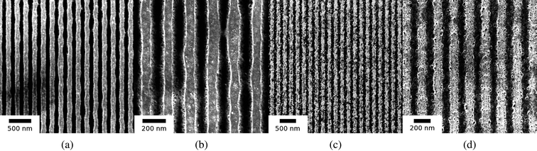 | ||
| Fig. 7 SEM images of nanowires from 42 nm film for two different Eo with the interference angle, θi = 86°, and 3000 laser pulses. (a) Eo = 440 mJ cm−2 and (b) magnified image of (a). (c) Eo = 535 mJ cm−2 and (d) magnified image of (c). | ||
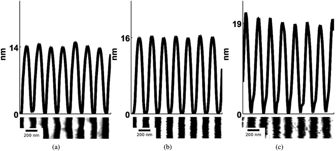 | ||
| Fig. 8 AFM line scans of the wire profiles of SnO2 nanowires formed from three different energy densities (a) Eo = 440, (b) Eo = 535 and (c) Eo = 700 mJ cm−2. The initial film thickness was 42 nm, the interference angle was 86°, and the number of laser pulses was 3000. The average for all measured nanowire height for each sample is (a) hnw = 14, (b) hnw = 16 and (c) hnw = 19 nm respectively. | ||
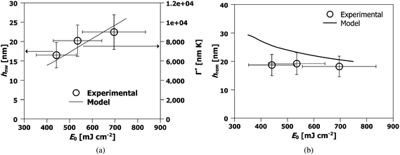 | ||
| Fig. 9 Behavior of hnw and hrem as a function of Eo for 42 nm films at an interference angle of 86° irradiated by 3000 pulses: (a) the experimentally determined nanowire height (open circles, left axes) and theoretically predicted behavior of the integrated evaporation difference Γ* between regions of maxim and minima (dashed line, right axes). (b) The experimentally measured (open symbols) and theoretically predicted (line) remaining film thicknesses hrem. | ||
Based on the SEM and AFM results presented above, one can conclude some general aspects about the mechanism of nanowire synthesis. First, evaporation appears to be playing an important role in the synthesis, as is evident from the lower film thickness remaining following the processing [Fig. 6 (b) and Fig. 9 (b)]. This observation of large evaporation is also important in the context of the chosen energy densities, which were close to the melt threshold energy of the SnO2 films. Secondly, the wire height (and aspect ratio) increase with increasing initial film thickness as well as increasing energy density. Finally, the self-limiting effect on wire formation needs to be explained. In this effect, wire formation appears to stop when the remaining film thickness achieves a stable value shown in Fig. 6 (b) and Fig. 9 (b). In order to understand these aspects, we have resorted to finite element calculations of the nanosecond pulsed laser interference heating of the SnO2 films to determine the temperature behavior as a function of film thickness and laser energy density.
3.2. Thermal model
In order to better understand the mechanism responsible for the formation of nanowires, an optical and thermal model was constructed to determine the temperature evolution of a multilayer system comprised of an SnO2 thin film on a SiO2/Si substrate irradiated by uniform as well as interfering laser beams. The first step in creating this model, shown schematically in Fig. 10 (a), is to accurately determine the optical properties of all the materials involved, in this case the SnO2 films, and the SiO2 and Si substrate components. The values of the complex refractive index, N, at λ = 266 nm is reported as NSiO2 = 1.4585 and NSi 1.831–4.426i for the substrate materials.28,30 The optical properties of SnO2 at λ = 266 nm measured by Jimenez et al. is N = 2.04–0.2i, and implies that SnO2 films should be nearly transparent for the thicknesses and wavelengths used in this work, making pattern formation by laser-thermal heating very difficult. However, it was mentioned by the same authors in ref. 31 that the index may vary significantly depending on the method of film deposition.31 To address this, experimental values of reflectivity, R, and transmissivity, T, for SnO2 films of various thickness (15, 25, and 90 nm) prepared on 750 μm quartz substrates was measured. The experimental R and T were compared to theoretical values calculated under the assumption of coherent layers.32 Using a simple least squares optimization of the data, we determined that the best fit of N = 2.0 − 0.97i yielded a reasonably good agreement between the measured and theoretical values of R and T, as shown in Fig. 10 (b) and (c) respectively.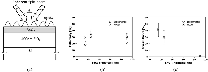 | ||
| Fig. 10 (a) Schematic of geometry used for the optical + thermal model. (b) The measured reflectivity, and (c), transmittance (open symbols) of known thicknesses of SnO2 deposited on 750 μm quartz from optical spectroscopy. The best fits (crosses) were modeled using NSnO2 = 2.0 − 0.97i. | ||
The next step to an accurate model was to find the time and position dependent energy absorption within the multilayer SnO2/SiO2/Si system when irradiated by pulsed laser in interference. The method outlined by Prentice32 was modified by including the angle dependent reflectivity at the interfaces.33 Following the same method, and accounting for the two beam interference pattern while applying a position dependent phase change to each beam and adding the normalized resultant electric field, E, the resultant absorption profile for a SnO2/400 nm SiO2/Si film stack can be determined.33 The resulting normalized absorption profile is given as  , where α is the absorption coefficient of the film, |Ei| is the modulus of the average incident electric field, and |E(x,z)| is the modulus of the resultant electric field within the film which varies as a function of the lateral dimension, x, due to the interference pattern and the depth, z, due to absorption and reflection effects. The normalized absorption as a function of depth (z) is shown in Fig. 11 (a), for x position corresponding to the maximum incident intensity due to complete constructive interference. The two-beam interference pattern assuming 36° off normal incidence (72° between the beams) is shown as the normalized surface absorption profile in Fig. 11 (b), but this characteristic shape may be found for any depth. Assuming a Gaussian pulse shape, the total volumetric rate of energy absorption is given by:
 .23
.23
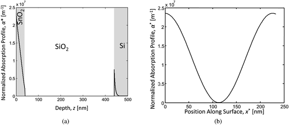 | ||
| Fig. 11 Absorption profiles of the SnO2/SiO2/Si stack for the case of: (a) complete constructive interference depth profile and (b) surface absorption profile. | ||
This model was then applied to a 2–D thermal finite element analysis (COMSOL) including characterization of the melting of the SnO2 film, as was conducted by Trice et al. to determine the temperature evolution at every point in the film stack.23 The thermal conductivity of SiO2 was taken as the non-radiative thermal conductivity since the length scales involved are significantly shorter than wavelengths involved in radiative transport.34,35 The temperature dependent heat capacity of SnO2 was determined from Pankratz36 and density from Taylor.37 Due to the lack of data, only the room temperature thermal conductivity of SnO2, k = 10 Wm−1K−1, was available, so this value was taken as temperature independent.38 The remaining thermal properties of SiO2, and those of Si were taken as the temperature dependent functions given in a material constants handbook.39 The melting temperature of SnO2 (1903.2 K) and the enthalpy of fusion (155.3 J g−1) were employed to model the phase change by an effective heat capacity technique.23,39 A complete list of the optical and thermal properties used for this simulation are given in Table 1 and Table 2, respectively. Verification of the 2-D thermal model was performed by comparing the experimentally determined melt threshold for single beam irradiation at normal incidence of two samples of known thickness, which yielded 63 and 99 mJ cm−2 for 5 nm and 42 nm films respectively. These values compared favorably with the model, which predicted values of 60 and 91 mJ cm−2.

 [
[


Applying this model to the experimental conditions outlined previously, the temperature difference between interference maxima and minima of the liquid SnO2, ΔT, determined at the moment the entire film has melted is given in Fig. 12 (a). The film temperature at the maxima and minima of the interference pattern for the case of average incident energy per pulse of 400 mJ cm−2, is shown in Fig. 12 (b) as a function of film thickness. Clearly, the thickness of the SnO2 film has a profound effect on these temperatures. A non-monotonic variation in the temperature is seen, with a maxima occurring around a film thickness of 25 nm, and dropping sharply for thinner films. This type of temperature variation has been observed previously for ultrathin metal films on optically transparent substrates.23 The behavior arises from the nanoscale nature of laser-film heating and can be briefly explained here as follows.26,27 For the case of SnO2, the experimentally estimated skin depth δ at 266 nm wavelength is 21.8 nm (as obtained from the experimentally extracted k values). Consequently, for SnO2 films with thickness comparable to the skin depth, the intensity of light energy absorbed will vary exponentially with thickness as I(ho) = Io(1 − e−h0/δ), where Io is the incident light intensity. Secondly, the effective reflectivity of light from the surface of the SnO2 film on the SiO2 substrate is also strongly dependent on SnO2 film thickness. This can be understood physically by noting that at zero film thickness the reflectivity will be that of the SiO2 substrate (which is practically zero for UV light) while it will be the value of the bulk SnO2 (which is ≫ zero) for a very thick film. From the experimental measurements of reflectivity and estimated N values, a quantitative calculation based on evaluating the Fresnel coefficients for such SnO2/SiO2 bilayer systems yields the general nature of the thickness dependent reflectivity as R(ho) = ro(1 − exp(−arho)), where ar and r0 are materials-dependent parameters.33 Third, the effective mass of the material heated M(ho) is also a strong function of film thickness for the following reason. When the film thickness is less then one thermal conduction depth, any heat generated within the nanoscopic metal film due to optical absorption will diffuse into the underlying SiO2 substrate. Consequently, the effective mass of material heated will include the thermal mass of the film and an effective thermal mass of the substrate estimated from the length scale of thermal diffusion occurring within the substrate in the nanosecond time scales of the experiment. Therefore, the heated mass will be 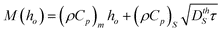 , where the subscript m and s denote metal and substrate while ρ and Cp are values of density and specific heat, DthS is the substrate thermal diffusivity and τ is the ns time scale of laser heating. Consequently, energy balance shows that the temperature rise will be qualitatively given by ΔT(ho) = I(ho)(1 − R(ho))τ/M(ho). As can be noted, in this function, I increases with increasing thickness while (1-R) and 1/M decrease with increasing thickness. As a result, a non-monotonic variation in temperature with film height ho can be expected for any given laser intensity and in fact at a critical film thickness the temperature rise will be a maximum. This behavior, as estimated from a more accurate finite element modeling, is shown in Fig. 12 (b). A maxima in temperature occurs around a film thickness of 25 nm, while there is a large rate of change in temperature with thickness for films on either side of this maxima.
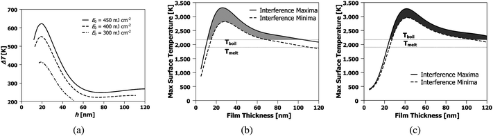 | ||
| Fig. 12 Thermal model results showing: (a) the temperature difference between the interference maxima and minima when the entire film has melted; (b) maximum surface temperature as a function of SnO2 film thickness for θ = 72° and Eo = 400 mJ cm−2; and (c) maximum surface temperature as a function of SnO2 film thickness for θ = 86° and Eo = 550 mJ cm−2. The shaded regions in (b) and (c) represent the integrated evaporation difference Γ*. | ||
4. Discussion and conclusion
The nanowire array may be formed by either liquid movement due to thermocapillary (TC) forces resulting from a temperature induced surface tension gradient, or preferential evaporation of the film between the regions of high intensity (constructive interference) and low intensity. As shown in Fig. 12 (a), the two beam irradiation causes a temperature disparity between the regions of constructive and destructive interference. Consequently, the surface tension gradient generates marangoni or thermocapillary flow along the plane. An estimate of magnitude of contribution of TC effects on fluid flow may be directly obtained from the characteristic time scale of TC flow τM. As shown in ref. 40, τM depends on the temperature gradient on the film surface, the film thickness ho, as well as materials parameters, and can be expressed as: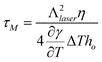 | (1) |
 , and this was used to estimate the TC time scale.41 For the case of Eo = 400 mJ cm−2 and ho = 50 nm, a temperate difference of ΔT = 530 K was obtained from thermal modeling for a fringe spacing of Λlaser = 225 nm (corresponding to θi = 72°). From this, the value of τM was estimated to be around 9 ns, which is comparable to the laser pulse time scale suggesting that it is reasonable to expect some contribution from TC flow under the two beam interference irradiation. However, at this stage, the experimental observations from wire formation cannot clearly differentiate between contributions from TC flow versusevaporation. Moreover, since we have observed substantial evaporation, it is also important to estimate the magnitude of contribution from preferential evaporation on the wire formation.
First, the maximum rate of evaporation at a given temperature can be estimated from the classical relation between pressure and temperature42 as:
 | (2) |
The thermal model can also be used to explain the behavior of hnw as a function of ho and Eo. In Fig.12 (b) and (c), the temperature difference between the regions of maxima and minima are shown as a function of starting film thickness ho for the 72 and 86° irradiation geometries respectively. As Fig.12 (b) and (c) show, evaporation will occur at the maxima and minima locations, but at different rates because of the different temperatures. For thick films (> 25 nm or so), this evaporation rate increases as the film thins. Now, as the temperature in the maxima continues to rise, the temperature in the minima will also begin to rise as a consequence of thermal diffusion. Consequently, the minimum also enters the evaporation zone and starts thinning. Now, a parallel thinning of the maxima and minima occur, albeit at slight different rates, as given by their respective temperatures. Finally, both locations thin enough such that the evaporation stops. From Fig. 12 (b) or (c), the two regimes can be seen to have slightly different evaporation cut-off thicknesses. If one assumes a constant evaporation rate for the entire film, so that the total evaporation time tevap ∝ h0 − heff, and if the local evaporation rate is assumed to be relative to the modeled T − Tboil, a relative measure of preferential evaporation may be determined by integrating the relative temperature difference that exists above the melting point and the thickness. This relative evaporation difference Γ* can be evaluated as:
 | (3) |
 | (4) |
From this discussion, the non-monotonic thickness-dependent temperature behavior provides opportunity to synthesize wires under a variety of interesting laser parameters. For instance, by varying the intensity of the individual interfering beams, it is possible to modulate the temperature difference between the maxima and minima. Hence, this can be used to influence hnw as well as the hrem. Another important aspect of the processing of SnO2 is the relatively small difference between the melting point and boiling point (i.e. 270 K). As a result, wire formation by pure thermocapillary flow requires stringent control on the laser energy as well as in the intensity of each of the interfering beams. These studies could form the basis for further investigations of wire formation in SnO2.
Another important issue concerns the difference in the morphology of the nanowires formed from the films with different initial thickness and/or at different laser energies. As seen from Fig. 4 and Fig. 7, the morphology can consist of a cluster of nanoparticles in contact with each other [Fig. 4 (a)], continuous smooth nanowires, [Fig. 7 (b)], or a porous nanowire structure [7 (d)]. We have found that the nanoparticle-like morphology occurs when synthesis is done starting with very thin films, typically near the final remaining thickness hrem. In this situation synthesis is dominated by melting and fluid flow rather then evaporation. We attribute this morphology behavior to the competition between liquid film morphology change due by dewetting competing with morphology from thermocapillary flow. It has been shown earlier for metal films that when the films are extremely thin, the time scale for film dewetting, which scales with thickness as τD ∝ h5, can be comparable to the thermocapillary time scale τM.25 Consequently, the observed morphology was a compromise between the two processes and resulted in nanoparticles arranged in rows. We suggest that a similar reasoning underlies the morphology seen in Fig. 4 (b), especially for the films with low starting thickness where the synthesis is dominated by melting and fluid flow, as compared to evaporation. On the other hand, the more porous structure seen for the thicker films processed at higher laser energies [Fig. 7 (d)] is possibly due to the relatively larger role played by evaporation in this synthesis regime.
In conclusion, we have synthesized parallel nanowire arrays of SnO2 on SiO2 substrates by nanosecond pulsed laser irradiation. Such nanowires are potential candidates for improved H2 sensor performance The array morphology was characterized by SEM and AFM, in conjunction with EDS and XPS measurements to evaluate concentration and stoichiometry. Due to evaporation, the final nanowire array had a lower effective SnO2 film thickness, whose value was independent of starting film thickness for any given laser energy density, but decreased with increasing energy density. Furthermore, a self-limiting effect was observed wherein the wire formation stopped at this effective remaining film thickness. These behaviors could be explained by nanoscale effects of the laser-film heating that resulted in a highly non-monotonic film temperature dependence on film thickness. In addition to the nanowire height, the structure of the nanowires was dependant on the amount of evaporation, with large initial thicknesses producing consistent nanowires and small thicknesses, where no evaporation takes place, producing clusters of nanoparticles in contact with each other. These results show that fabrication of large nanowire arrays can be achieved by careful analysis of the thermal behavior in conjunction with experiments.
Acknowledgements
The authors acknowledge support by the National Science Foundation through grants NSF-ECCS-0850574 and NSF-ECCS-0801774. RK also acknowledges support through CAREER grant DMI-0449258. NS and JS also acknowledge AFM measurements performed by P. Mreutesatorn. A portion of the research (XPS and XRD) was performed using EMSL, a national scientific user facility sponsored by the Department of Energy's Office of Biological and Environmental Research and located at Pacific Northwest National Laboratory.References
- N. M. Sammes and R. Boersma, Small-scale fuel cells for residential applications, J. Power Sources, 2000, 86(1–2), 98–110 CrossRef CAS.
- M. Mogensen, M. S. Nigel and G. A. Tompsett, Physical, chemical and electrochemical properties of pure and doped ceria, Solid State Ionics, 2000, 129(1–4), 63–94 CrossRef CAS.
- C. M. White, R. R. Steeper and A. Lutz, The hydrogen-fueled internal combustion engine: a technical review, Int. J. Hydrogen Energy, 2006, 31(10), 1292–1305 CrossRef CAS.
- B. S. Archanjo, G. V. Silveira, A.-M. B. goncalves, D. C. B. Alves, A. S. Ferlauto, R. G. Lacerda and B. R. A. Neves, Fabrication of Gas Nanosensors and Microsensors via Local Anodic Oxidation, Langmuir, 2009, 25, 602–605 CrossRef CAS.
- C. Drake, A. Amalu, J. Bernard and S. Seal, Enhancing the low temperature hydrogen sensitivity of nanocrystalline SnO2 as a funciton of trivalent dopants, J. Appl. Phys., 2007, 101, 104307 CrossRef.
- S. G. Ansari, P. Boroojerdian, S. R. Sainkar, R. N. Karekar, R. C. Aiyer and S. K. Kulkarni, Grain size effects on H2 gas sensitivity of thick film resistor using SnO2 nanoparticles, Thin Solid Films, 1997, 295(1–2), 271–276 CrossRef CAS.
- G. K. Mor, M. A. Carvalho, O. K. Varghese, M. V. Pishko and C. A. Grimes, A room-temperature TiO2-nanotube hydrogen sensor able to self-clean photoactively from environmental contamination, J. Mater. Res., 2004, 19(2), 628–634 CrossRef CAS.
- C. Wang, L. Yin, L. Zhang, Y. Qi, N. Lun and N. Liu, Large Scale Synthesis and Gas-Sensing Properties of Anatase TiO2 Three-Dimensional Hierarchical Nanostructures, Langmuir, 2010, 26, 12841–12848 CrossRef CAS.
- P. Tobiska, A. Hugon, A. Trouillet and H. Gagnaire, An integrated optic hydrogen sensor based on SPR on palladium, Sens. Actuators, B, 2001, 74, 168 CrossRef.
- C. K. Kim, J. H. Lee, Y. H. Lee, N. I. Cho and D. J. Kim, A study on a platinum-silicon carbide Schottky diode as a hydrogen gas sensor, Sens. Actuators, B, 2000, 66(1–3), 116–118 CrossRef.
- G. H. Lu, L. E. Ocola and J. H. Chen, Room temperature gas sensing based on electron transfer between discrete tin oxide nanocrystals and multiwalled carbon nanotubes, Adv. Mater., 2009, 21, 24.
- S. Shukla, S. Seal, L. Ludwig and C. Parish, Nanocrystalline indium oxide-doped tin oxide thin film as low temperature hydrogen sensor, Sens. Actuators, B, 2004, 97(2–3), 256–265 CrossRef.
- G. Zhang and M. Liu, Effect of particle size and dopant on properties of SnO2-based gas sensors, Sens. Actuators, B, 2000, 69(1–2), 144–152 CrossRef.
- A. Licciulli, S. Mazzarelli, G. De, P. Siciliano, L. Vasanelli and R. Rella, Os and pd modified tin oxide films for sensors by the sol gel process, J. Sol-Gel Sci. Technol., 2001, 21(3), 195–201 CrossRef CAS.
- T. F. Baumann, S. O. Kucheyev, A. E. Gash and J. H. Satcher, Adv. Mater., 2005, 17, 1546–1548 CrossRef CAS.
- M. Law, H. Kind, B. Messer, F. Kim and P. D. Yang, Photochemical sensing of NO2 with SnO2 nanoribbon nanosensors at room temperature, Angew. Chem., Int. Ed., 2002, 41, 2405–2408 CrossRef CAS.
- M. Batzill and U. Diebold, The surface and materials science of tin oxide, Prog. Surf. Sci., 2005, 79, 47–154 CrossRef CAS.
- Z. Fan, J. C. Ho, T. Takahashi, R. Yerushalmi, K. Takei, A. C. Ford, Y. Chueh and A. Javey, Toward the development of printable nanowire electronics and sensors, Adv. Mater., 2009, 21, 3730–3743 CrossRef CAS.
- H. M. van Driel, J. E. Sipe and J. F. Young, Laser-induced periodic surface structures on solids: a universal phenonmenon, Phys. Rev. Lett., 1982, 49(26), 1955–1959 CrossRef CAS.
- S. E. Clark and D. C. Emmony, Ultraviolet-laser-induced periodic surface structures, Phys. Rev. B:, 1989, 40(4), 2031–2043 CrossRef CAS.
- D. Bauerle, Laser Processing and Chemistry. Berlin: Springer, second ed., 1996 Search PubMed.
- S. J. Henley, J. D. Carey and S. R. P. Silva, Pulsed-laser-induced nanoscale island formation in thin metal-on-oxide films, Phys. Rev. B, 2005, 72, 195408 CrossRef.
- J. Trice, D. G. Thomas, C. Favazza, R. Sureshkumar and R. Kalyanaraman, Investigation of pulsed laser induced dewetting in nanoscopic Co films: Thermal modeling and experiments, Phys. Rev. B: Condens. Matter Mater. Phys., 2007, 75, 235439 CrossRef.
- Y. Wu, J. D. Fowlkes, P. D. Rack, J. A. Diez and L. Kondic, On the Breakup of Patterned Nanoscale Copper Rings into Droplets via Pulsed-Laser-Induced Dewetting: Competing Liquid-Phase Instability and Transport Mechanisms, Langmuir, 2010, 26, 11972–11979 CrossRef CAS.
- C. Favazza, J. Trice, R. Kalyanaraman and R. Sureshkumar, Self-organized metal nanostructures through laser-interference driven thermocapillary convection, Appl. Phys. Lett., 2007, 91, 043105 CrossRef.
- J. Trice, C. Favazza, D. Thomas, H. Garcia, R. Kalyanaraman and R. Sureshkumar, Novel self-organization mechanism in ultrathin liquid films: theory and experiment, Phys. Rev. Lett., 2008, 101(1), 017802 CrossRef.
- H. Krishna, N. Shirato, C. Favazza and R. Kalyanaraman, Energy driven self-organization in nanoscale metallic liquid films, Phys. Chem. Chem. Phys., 2009, 11, 8136–8143 RSC.
- I. H. Malitson, Interspecimen comparison of the refractive index of fused silica, J. Opt. Soc. Am., 1965, 55, 1205 CrossRef CAS.
- T. Jean-Marc, C. Mohammed, H. Luc, L. Philippe, D. Jacques and G. Jean-Marie, Characterization of tin oxides by X-ray-photoemission spectroscopy, Phys. Rev. B, Jul 1992, 46, 2460–2466 Search PubMed.
- Handbook of Optics, vol. 2. McGraw-Hill, 2 ed., 1994 Search PubMed.
- V. M. Jimenez, J. P. Espinos, A. Caballero, L. Contreras, A. Fernandez, A. Justo and A. R. Gonzalez-Elipe, SnO2 thin films prepared by ion beam induced CVD: preparation and characterization by X-ray absorption spectroscopy, Thin Solid Films, 1999, 353, 113 CrossRef CAS.
- J. S. C. Prentice, Coherent, partially coherent and incoherent light absorption in thin-film multilayer structures, J. Phys. D: Appl. Phys., 2000, 33, 3139–3145 CrossRef CAS.
- O. Heavens, Optical Properties of Thin Solid Films. Dover Publications, 1991 Search PubMed.
- L. W. Kurt and J. C. Thomas, Thermal conductivity of clear fused silica at high temperatures, J. Appl. Phys., 1959, 30, 1702 CrossRef.
- P. Bouchut, D. Decruppe and L. Delrive, Fused silica thermal conductivity dispersion at high temperature, J. Appl. Phys., 2004, 96, 3221 CrossRef CAS.
- L. B. Pankratz, US Bureau of Mines Bulletin 672, 1984, p. 30 Search PubMed.
- D. Taylor, Trans. J. British Ceramic Soc., 1984, 83, 32 Search PubMed.
- P. Tiirkes, J. Phys. C: Solid State Phys., 1980, 13, 4941 CrossRef.
- CRC Handbook of Chemistry and Physics, 2009 Search PubMed.
- T. Schwarz-Selinger, D. G. Cahill, S.-C. Chen, S.-J. Moon and C. P. Grigoropoulos, Micron-scale modifications of Si surface morphology by pulsed-laser texturing, Phys. Rev. B: Condens. Matter, 2001, 64, 155323 CrossRef.
- C. Yaws, ed., Chemical Properties Handbook. McGraw-Hill, 1999 Search PubMed.
- M. Ohring, The Materials Science of Thin Films, Harcourt Brace jovanovich, 1992 Search PubMed.
- P. D. Desai, J. Phys. Chem. Ref. Data, 1986, 15, 967 CrossRef CAS.
- K. K. Kelley, US Bureau of Mines Bulletin 476, 1949, p. 42 Search PubMed.
- C. F. Lucks, H. W. Deem and W. D. Wood American, Ceram. Soc. Bull., 1960, 39, 313 CAS.
- L. van Vlack, Physical Ceramics for Engineers. Addison-Wesley Publishing Co., 1964 Search PubMed.
| This journal is © The Royal Society of Chemistry 2011 |