Small-sized silicon nanoparticles: new nanolights and nanocatalysts
Zhenhui
Kang
*ac,
Yang
Liu
*ac and
Shuit-Tong
Lee
*b
aInstitute of Functional Nano & Soft Materials Laboratory (FUNSOM) and Jiangsu Key Laboratory for Carbon-Based Functional Materials and Devices, Soochow University, Suzhou, China. E-mail: zhkang@suda.edu.cn; Yangl@ suda.edu.cn
bCenter of Super-Diamond and Advanced Films (COSADF), City University of Hong Kong, Hong Kong, SAR, China. E-mail: apannale@cityu.edu.hk
cFaculty of Chemistry, Northeast Normal University, Changchun, Jilin 130024, China
First published on 16th December 2010
Abstract
Owing to their abundant unique properties and ready compatibility with Si microelectronic technology, Si nanostructures are becoming one of the most important classes of nano semiconductors. Particularly, small-sized Si nanoparticles possess distinctive photoluminescence (PL), biocompatibility, and active surface properties. In this review, we focus on the synthesis and PL properties of small-sized Si nanoparticles and their potential applications in the fields of bioimaging and nanocatalysis. We further highlight major challenges and promises in this area.
 Zhenhui Kang | Zhenhui Kang is currently a Professor in the Institute of Functional Nano & Soft Materials and the Jiangsu Key Laboratory for Carbon-Based Functional Materials & Devices in Soochow University, P. R. China. His main research interests are in the areas of the shape control of multifunctional materials (carbon/silicon, polyoxometalates, ionic liquids) and their photoluminescence, catalytic and bio-imaging applications. |
 Yang Liu | Yang Liu is currently an Associate Professor in the Institute of Functional Nano & Soft Materials and the Jiangsu Key Laboratory for Carbon-Based Functional Materials & Devices in Soochow University, P. R. China. Her current research interests include morphologically unique nanostructures and nanocomposites for catalysis and energy conversion. |
 Shuit-Tong Lee | Shuit-Tong Lee is a member (academician) of the Chinese Academy of Sciences (CAS) and fellow of the academy of sciences for the developing world (TWAS). He is a Chair Professor of Materials Science and Director of the Center of Super-Diamond and Advanced Films (COSDAF) at City University of Hong Kong, Director of FUNSOM at Soochow University, and Director of Nano-Organic Photoelectronic Laboratory at the Technical Institute of Physics and Chemistry, CAS. His major research areas include functional nanomaterials and devices, organic electronic materials and technologies, diamond and super-hard thin film technologies. |
1. Introduction
The properties of silicon (Si) are generally understood based on atomic and bulk Si models.1 Because of the benign, abundant and inexpensive nature of Si materials, the expansion of Si usages in electronic, optoelectric, biological and other diverse applications is highly desirable.2–4 Due to their diverse properties (e.g. size-dependent emission and band gap, biocompatibility, and high-sensitivity and reactive Si–H surface) and the huge Si microelectronics market, Si nanostructures are gradually becoming one of the most important classes of nano-semiconductors in the sensor, electronic, optic, and catalysis fields.5–16Si is an indirect band gap semiconductor with a low probability for phonon-assisted, radiative electron–hole recombination (i.e. resulting in the spontaneous emission of photons). Nevertheless, there is global research interest in developing a Si light-emitting diode, ultimately Si-based lasers, and in looking at the photoluminescence (PL) properties of nanoscale Si particles. As there are already a number of comprehensive reviews on Si photonic or light-emitting devices,3,4,17–20 in this review we shall concentrate instead on the active research of intense current interest in nanoscale Si materials; i.e. their PL properties and applications in the fields of imaging and catalysis.
In general, small semiconductor particles show large size-dependent changes in their spectroscopy below a particle radius of a few nanometres21 due to quantum confinement effects. The critical particle radius is characteristic of the material, and is typically ∼5 nm for Si.21–24 Among the quantum-sized Si nanostructures, porous Si is a special case which consists of fine filaments each a few nanometres across and can luminesce intensely in the visible range at room temperature. The emission mechanism of porous Si has been reviewed extensively,13–15,22–24 although it still remains somewhat controversial.24 Here we focus on separated and individual small-sized Si nanoparticles (SS SiNP), small-diameter Si nanowires (SiNWs), and Si dots of a few nanometres in diameter. We adopt the terminology of “Si nanowires” to include nanowires and wirelike and rodlike Si crystals with a diameter of less than 100 nm.
It should be noted that SS SiNPs are much less well understood in terms of their fundamental photophysics than the particles of direct gap semiconductors.21,24 The PL properties of Si nanoparticles are currently an area of much research interest. There are already a few applications of Si nanoparticles based on PL properties. While the PL properties of the SS SiNPs are not completely understood, already there is growing evidence that the PL is size-dependent and strongly affected by surface modification.2,4,8,16 In this review, by introducing the synthesis and PL properties of the SS SiNPs (with active surface and good biocompatibility) we hope to provide insight and stimulate further research into their properties and potential applications, especially in bioimaging and nanocatalysis (see Scheme 1).
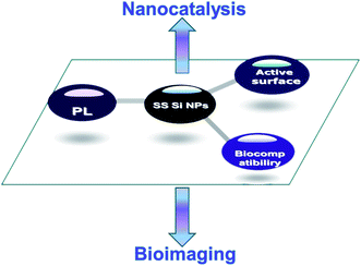 | ||
| Scheme 1 SS SiNPs with unique PL, biocompatibility, and active surface properties have great potential applications in bioimaging and nanocatalysis. | ||
2. Synthesis and surface functionalization
2.1 Synthesis techniques of Si dots
Si dots can be prepared by various routes, such as physical, physicochemical, chemical, and electrochemical procedures.2 Physical routes typically involve high-temperature and vacuum deposition techniques and are used to produce small quantities of materials for physical or electronic applications. Chemical routes tend to produce larger amounts of material, although less well-defined in terms of composition and size, which can be readily conjugated to functional molecules.16 Porous Si is generally considered as a nanocrystalline film which can be broken up into individual nanoparticles by various means, including ultrasonication. As there is a large number of reviews on porous Si and its surface chemistry, we discuss here primarily the preparations of samples consisting of isolated Si dots.For particle size control, Kang et al. have developed a polyoxometalate (POM)-assisted electrochemical method, which yielded highly monodisperse Si dots (∼1, ∼2, ∼3, and ∼4 nm) with a narrow size distribution requiring no further separation. In addition, this method also could realize the controlled synthesis of a variety of Si nanostructures, ranging from Si nanoparticles (SiNPs), SiNWs, to ordered Si micro-/nano-structures (see Fig. 1 and 2).8 It represents a convenient and rational synthesis of a variety of Si nanostructuresvia the simple control of current density and choice of catalyst POMs. POMs clearly play a vital role in controlling the size of Si dots and formation of Si nanostructures. The size control of Si dots may be attributed to the unique electronic characteristics of POMs in gaining and donating electrons simultaneously while keeping their structure unchanged (see Fig. 2a).51–56
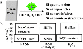 | ||
| Fig. 1 (a) Si quantum dots, nanoparticles, nanowires, and ordered Si complex micro-/nano-structures can be obtained directly from Si wafer by a polyoxometalate-assisted electrochemical method. (b) The relationship between the current density, catalyst, and the products. (Reprinted with permission from ref. 8, © 2007 American Chemical Society.) | ||
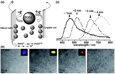 | ||
| Fig. 2 (a) Schematic for the POM-assisted electrochemical etching process. (b) Transmission electron microscopy (TEM) image of a serial of SiQDs and their corresponding luminescence colors under UV irradiation (inset). (c) Typical PL spectra of SiQDs with sizes ranging from ∼1 to ∼4 nm. (Reprinted with permission from ref. 8, © 2007 American Chemical Society.) | ||
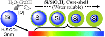
Kang et al. also achieved the conversion of ∼3 nm H–Si dots to water-soluble, uniform Si dots (or Si/SiOxHy core–shell nanostructures in solution) of different core sizes via controlled oxidation in EtOH–H2O2 solution.57 The uniform-sized Si dots of different diameters can be finely tuned to emit in seven different colors due to emission from the quantum-sized Si cores (see Fig. 3).57
2.2 Synthetic techniques of SiNWs
As a special form of one-dimensional Si nanostructures, SiNWs are particularly attractive. Research on SiNWs has developed rapidly in recent years.6,7,14,15 Typically, two main fabrication routes have been adopted for SiNWs. The first one is a top-down approach, based on Si wafer processing by means of an etching technique. The second one is a bottom-up approach, such as chemical-vapor deposition (CVD), thermal vaporization of SiO, molecular beam epitaxy (MBE), laser ablation, and solution-based techniques.2,14,15 All techniques yield wires with different orientations and diameters. The smallest SiNW diameter reported so far is 1.2 to 5 nm,2,6 while experiment and theory clearly show that substantive quantum size effects emerge in SiNWs with diameters of 3 nm and below.2,6,14,15,58–60For the CVD method, it is crucial to reduce the oxygen background pressure in order to be able to epitaxially grow uniform SiNWs. The low growth pressures depend mainly upon the gaseous Si precursor and its cracking probability at the catalyst surface, which allows the combination of CVD with the transmission electron microscopy (TEM) technique, enabling in situ observation of the nanowire growth.14,15,74–76CVD can allow epitaxial growth of SiNWs, with the growth velocity depending on temperature and type of Si precursor used. CVD offers the broad possibility of modifying the properties of SiNWs in a controlled fashion. Another advantage of CVD is the wide variability of wire sizes (length and diameter).14,15,77,78 Further, CVD offers the opportunity of controlled doping via addition of doping precursors during growth. By switching the doping precursor, modulating doping profiles in axial direction can be created.14,15,79–82
One of the problems of SiNWs grown by CVD is the variation of the growth direction, especially for wire diameters smaller than about 50 nm.14,15,83 This obstacle may be circumvented by growing the nanowires in a template, such as anodic aluminium oxide (AAO).14,15,84–86
In principle, two different growth mechanisms are possible: growth with and without metal catalyst.14,15,88Growth assisted by the presence of a metal catalyst is relatively rapid.14,15,88 Consistent with the concept of VLS growth, the wire diameters are determined by the size of the catalyst particle, although the interplay between the nanowire and the catalyst droplet seems to be more complex compared to normal CVD growth.2,6,14,15 As a consequence of the disproportionation of SiO, the diameter ratio between crystalline Si core and amorphous oxide shell remains approximately constant.14,15,89 The second growth mode, metal-catalyst-free growth, has been originally proposed for SiNW growthvialaser ablation,14,15,90 in which the nanowires can be catalyzed by Si oxide, so-called oxide-assisted growth (OAG).14,15,91
In the oxide-assisted growth (OAG), oxide (SiO)-containing targets clearly raise the yield of SiNWs compared to pure Si or mixed Si-metal targets.14,15,90 By carrying out the growth process over several hours, one can obtain millimetre-long crystalline SiNWs with varying diameters of 5–100 nm, covered with an amorphous oxide shell of several 10 nm.6,14,15
The detail atomic structure and energy gaps of small-diameter SiNWs have been measured by Ma et al.6 The small-diameter (1 to 7 nm) SiNWs were prepared by OAG method, and their surfaces were removed of oxide and terminated with hydrogen by a hydrofluoric acid dip. Scanning tunneling microscopy (STM) of these SiNWs,6 performed both in air and in ultrahigh vacuum, revealed atomically-resolved images of hydrogen-terminated Si surfaces corresponding to SiH3 on Si (111) and SiH2 on Si (001), respectively (see Fig. 4). Importantly, hydrogen-terminated SiNW surfaces are more oxidation-resistant than regular silicon wafer surfaces. The energy gaps of small-diameter SiNWs were found to increase with decreasing SiNW diameter from 1.1 eV for 7 nanometres to 3.5 eV for 1.3 nanometres, confirming previous theoretical predictions.
![Constant-current STM image of a SiNW with small diameter prepared via the OAG method. The wire axis is along the [112] (left) and [110] (right) direction. Scale bar: 1 nm. (Reprinted with permission fromref. 6, © 2003 Science.)](/image/article/2011/NR/c0nr00559b/c0nr00559b-f4.gif)
2.3 Surface functionalization
Surfaces of Si nanoparticles may constitute the chemical analogue of continuous surfaces (Si flat and porous Si wafers).2,7 However, they have several particularities which require the adjustment of the modification strategies applied to bulk Si surfaces. The reactivity of the nanosurface can be higher than that of the surface of the bulk material due to a higher surface curvature and consequently more defective surfaces composed of stressed Si–Si bonds. For instance, ultrasmall (∼1 nm) Si nanoparticles have a highly emissive surface on which excited excitons are self-trapped.2,7,122–125 We discuss the surface functionalization of Si dots and Si NWs together due to their similarity.The chemistry chosen for surface modification should involve the replacement of the hydrogen of Si–H groups.2,7,122,123 In general, a SiO2 overlayer completely inhibits the chemical activity of Si. On the other hand, Si–H and Si–Si bonds on the particle surface can be reactive. On ultrasmall species, Si–O bonds may increase the reactivity of the Si nanosurface because these bonds tend to polarize the Si–Si and Si–H bonds, rendering them more amenable to functionalization.2,7 Typically, H-terminated Si surfaces could be halogenated, could react with alkanes and alkenes under metal catalysis, form Si–C bonds under light or heat, and react with aldehyde groups to form Si–O bonds.126–128Si nanoparticles have been functionalized with alcohol, butylamine, 1-pentene, carboxylic acid, thiol groups, etc.129,130 Thermally activated reactions of several alcohols with Si nanoparticle colloid in toluene have been shown to result in the formation of alkoxy-coated particles.2,131 The modified particles exhibited superior qualities, with lower oxidation level.2 Organic alkyl-monolayer-coated nanoparticles may be synthesized directly during liquid solution-phase synthesis utilizing molecular Si compounds via Si–C linkage.2,132–137 The aminization of particles was accomplished via a Si–N linkage.2,132–137Pentene reacted with Si nanoparticlesvia a Si–C linkage. Carboxylic groups formed on the surface of small H-passivated Si nanoparticles through reaction with derivatives of organic acid via a Si–C linkage.2,132–137 Since both COOH and C![[double bond, length as m-dash]](https://www.rsc.org/images/entities/char_e001.gif) C groups are prone to react with Si particles under hydrosilylation conditions, the acid group was ester-protected during the reaction.
C groups are prone to react with Si particles under hydrosilylation conditions, the acid group was ester-protected during the reaction.
Notably, Si nanoparticles, especially Si quantum dots, have been modified and transformed into Si nanospheres to achieve the desired functionalities. Recently, Lee and coworkers developed a strategy for the synthesis of fluorescent, size-controllable Si nanospheres (see Fig. 5).8,9,12,13 These nanospheres can be readily produced by a UV irradiation-induced reaction between acrylic acid and Si quantum dots. The UV irradiation time is critical for controlling the size distribution of nanospheres. Significantly, compared to the original Si dots, the nanospheres are water-dispersible, stronger in fluorescent intensity and better in terms of photostability, and thus are potentially suitable for use as biological imaging probes. Further, Lee et al. also developed a thermal oxidation route by which the Si nanospheres were partially oxidized and transformed into a water-dispersed and pH stable oxidized Si nanosphere.8,9,12,13
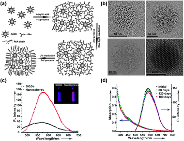 | ||
| Fig. 5 (a) Schematic of synthesis of Si nanospheres. (b) TEM images of three nanospheres with a size of ∼60 nm (top left), ∼120 nm (top right), and ∼200 nm (bottom left), and high-resolution TEM (HRTEM) image (bottom right) of a single SiQD inside the nanospheres. (c) PL of the free-standing SiQDs and as-prepared nanospheres, and (inset) the corresponding photograph of the luminescence from the samples of the free-standing SiQDs and nanosphere solution under irradiation by 365 nm light from UV lamp. (d) Temporal evolution of the absorption and corresponding PL spectra of the as-prepared nanospheres over half a year in ambient air conditions without any special protection. (Reprinted with permission from ref. 13, © 2009 Wiley.) | ||
SiNWs can be readily modified with metal nanoparticles. SiNWs surfaces can be hydrogen terminated after removing the oxide layer with HF or NH4F aqueous solution. The H-terminated SiNWs possess relatively high chemical reactivity, which can reduce many kinds of metal ions (such as Ag+, Au3+, Pd2+, Cu2+, etc) and organic species like chloroform and dichloromethane.2,7,138
3. PL properties of Si dots and SiNWs
3.1 PL properties of Si dots
The classic signature of quantum confinement is the observation of size-dependent optical absorption or PL.2,16,139,140 The studies of the optical properties of small-sized Si nanoparticles led to some controversy over the assignment of the transition responsible for the photoluminescence, and the details are still not settled. Nevertheless, some aspects are well recognized and established, which are briefly reviewed here for their relevance to the design of Si-based luminescent probes and catalyst.Using a pulsed CO2 laser to pyrolyze silane in a gas flow reactor and a molecular-beam chopper synchronized to the laser, Ledoux et al. were able to separate Si nanoparticles by size and showed clearly the blue-shift of the luminescence peak with particle diameter.140 In the range of particle diameters from 3 to 8 nm, their results matched rather well the theoretical curve calculated on the basis of an LCAO treatment, i.e.E = Ebulk + 3.73d − 1.39, where d is the particle diameter, E the energy (in eV) of the luminescence peak, and Ebulk is the bulk band gap.16,141 The smaller particles emitted lower photon energies than expected, which was attributed to traces of oxide leading to a level in the band gap of porous Si that limits the maximum observed PL energy to about 2.1 eV.16,142
More sophisticated electronic structure calculations have been made for particles greater than ∼2.5 nm in diameter, showing that the PL energy can be understood on the basis of quantum confinement.16 For smaller particles, the surface termination (and especially the role of oxygen) becomes more important because the large increase in the number ratio of surface to bulk Si atoms. Two effects should be considered: (i) traces of oxide introduce mid gap states, and (ii) complete O-termination of the surface can drastically alter the properties of the HOMO and LUMO.2,16 The first effect is thought to explain why porous Si structures prepared under anaerobic conditions emit blue light, but emit red light upon exposure to oxygen.2,16,142 The second effect has been studied by density functional theory looking at HOMOs and LUMOs.2,16,143 The computational studies clearly show that in small particles the surface has to be considered explicitly, and it is not sufficient to regard it as simply a boundary condition on the wavefunction of electrons in the core of the particle. As the particle diameter increases, the orbitals are increasingly determined by the core Si atoms and the simple quantum confinement models work better. However, the assignment of PL spectra of Si nanoparticles is still not settled, because the experimental literature shows examples of blue luminescence from C-implanted porous Si, oxidized porous Si/Si nanoparticles, and in fact, even in bulk SiO2.2,16,144–147 Further, it is quite common for oxidation of Si nanoparticles to cause a shift in the PL from red to blue.2,16,148,149
Using the electrochemical method Kang et al. produced highly monodisperse Si quantum dots (∼1, ∼2, ∼3, and ∼4 nm) with a narrow size distribution.8,9 The PL results showed that ∼1 nm particles emit a blue band at 450 nm and a weak structureless tail at 500–700 nm, ∼2 nm particles an intense green peak at 520 nm, ∼3 nm particles an intense red band at 640 nm, and ∼4 nm particles an infrared band at 740 nm. The red shift of the PL band with increasing Si quantum dots size and the larger band energy than the Si indirect band gap of 1.1 eV demonstrate distinctly the quantum confinement effect on the band gap energy in Si quantum dots smaller than 4 nm. Further, Kang et al. showed that controlled oxidation of ∼3 nm H–Si quantum dots can tune the Si core size, so that the resulting oxidized Si quantum dots can yield fine wavelength-tunable photoluminescence (see Fig. 6).8,9,57
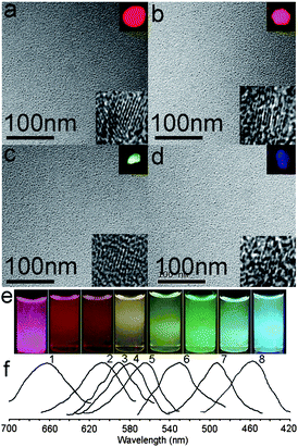 | ||
| Fig. 6 (a) TEM images of ∼3 nm H-SiQDs. (b–d) TEM images of SiQDs after oxidation of 0.5, 3.5, and 24 h, respectively. Insets are the corresponding fluorescent microscope and HRTEM images. (e) Photograph (under UV light) of H-SiQDs (left, red emission) and water-soluble SiQDs (yielding seven distinct emission colors). (f) PL spectra of H-SiQDs (curve 1) and SiQDs (curves 2 to 8) after 0.5, 1.5, 3.5, 6, 9, 14, and 24 h oxidation, respectively (excitation wavelength: 360 nm). (Reprinted with permission from ref. 57, © 2009 Wiley.) | ||
The above reports show that the PL properties of Si dots are still not well understood, and neither the observation of blue or red luminescence nor a determination of elemental composition is sufficient to deduce the nature of the PL transition: a detailed photophysical and spectroscopic study is required for each kind of new Si dot.2,8,9,16,57
3.2 PL properties of SiNWs
Compared to Si dots, there are fewer reports on the PL properties of SiNWs, and very little understanding of the emission mechanism. Here, we introduce some relevant reports on the PL properties of SiNWs.Sham et al. have found X-ray and vacuum ultraviolet excited PL to be of use in the assignment, because the initial absorption involves localized electronic states and can be correlated with the photoemission spectra.150,151 The blue PL in alkylated Si nanoparticles, prepared by an electrochemical method and subsequently oxidized, was determined to originate from excitation of oxidized Si atoms.149
The room-temperature PL from TiSi2-catalyzed SiNWs is attributed to the recombination of quantum-confined charge carriers in crystalline Si. In addition, the detailed PL studies show a blue shift and a reduction in PL lifetime with decreasing diameter, which is in agreement with the experimental and theoretical studies on Si nanostructures in the literature.152
For oxide-passivated SiNWs, a specific red PL at 745 nm was observed, and this peak may originate from the Si–O–Si bridge bonds along the wire direction (111) based on the theoretical calculation. With narrowing wire diameter or increasing length, the intensity of this peak is enhanced due to the increase in the density or total number of these bonds. This peak is not observed from other structures such as (110) or (112) SiNWs, implying its dependence on the crystalline configurations.153
Sa'ar and Lee et al.154 reported the cathodoluminescence (CL) imaging (see Fig. 7) and time-resolved PL spectroscopy (see Fig. 8) of moderate-size SiNWs (20–50 nm), which indicated that the origin of the luminescence may come from interface states and radiative centers in the cladding layer of the SiNWs. From time-resolved PL spectroscopy they found that the PL decay times of hydrogen-terminated SiNWs are two orders of magnitude faster than oxygen-terminated SiNWs. This result indicated the crucial role of surface chemistry in determining the luminescence properties of SiNWs. They also reasoned that quantum confinement effects cannot be responsible for the red emission band since the diameters of the SiNWs studied here are larger than the excitonic radius of the electron–hole pairs.154
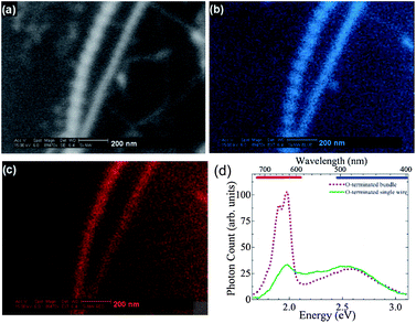 | ||
| Fig. 7 (a) High-resolution scanning electron microscopy (HRSEM) image of single SiNWs. (b) The corresponding pseudocolor blue CL image of the same SiNWs. (c) The corresponding pseudocolor red CL image. (d) CL spectra of the bundle of O-terminated as-grown SiNWs; the horizontal bars at the top represent the transmittance regions of the red and blue color filters used for quasimonochromatic CL imaging. (Reprinted with permission from ref. 154, © 2007 The American Physical Society.) | ||
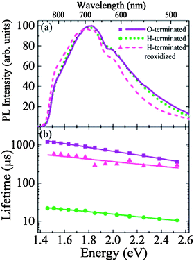 | ||
| Fig. 8 (a) PL spectra and (b) PL lifetimes of O-terminated, H-terminated, and reoxidized SiNWs. (Reprinted with permission from ref. 154, © 2007 The American Physical Society.) | ||
Recently, Rosenberg and Sham et al. utilized the chemical sensitivity of X-ray excited optical luminescence (XEOL) to determine the origin of overlapping emission bands in SiNWs. Using time-gating they refined the emission spectra and were able to determine the chemical nature of the emission bands falling within a specific time window. By performing Si K-edge X-ray excitation measurements, they have determined that the short lifetime components have a primarily Si character, while the long lifetime component stems from the SiO2 shell and SiO–Si interface.155
4. Applications in bio-imaging
Generally, luminescent probes for biological imaging should emit in the spectrum not absorbed by cells and should be water-soluble, highly emissive, and stable.2,16 The unique advantages of size-tunable fluorescent wavelength by a single wavelength excitation mean that quantum dots have a great potential for applications in optical encoding detection.12,13,16,57 To date, much emphasis has been placed on using highly-fluorescent II–IV quantum dots (CdSe and CdS, etc.) with wavelength-tunable emission as biological chromophores. However, these quantum dots may be cytotoxical due to release of Cd ions, thus their biological applications are doubtful.16,57Si is inert, nontoxic, abundant, low-cost, biocompatible, and widely used in microelectronics. Particularly, the various unique PL properties make the small-sized Si particles promising candidates for bio-imaging. For biomedical applications, it is desirable for Si quantum dots to have (i) a substantial PL quantum yield in the visible region and (ii) be water-soluble and hydrophilic to prevent aggregation and precipitation in a biological environment.12,13,16,57,1564.1 Bio-imaging of Si dots
The few studies on the bio-imaging of Si dots already suggested that the modified Si dots may be excellent candidates for bio-imaging. For example, Li and Ruckenstein157 used UV-induced graft polymerization of acrylic acid on the surface of Si dots to prepare stable aqueous luminescent Si dots. By grafting a water-soluble polymer on the particle surface, the dispersions in water of the Si dots became very stable and clear aqueous solutions can be obtained. Further, the surface modification not only increased the dispersibility but also improved the PL stability of the Si dots against degradation by water. They further used the surface-modified Si dots as biological labels for cell imaging.16,157Warner et al. described a simple room-temperature synthesis to produce water-soluble Si dots that exhibited strong blue PL and a rapid rate of recombination.156Si dots with a narrow size distribution were synthesized using reverse micelles and powerful hydride reducing agents at room temperature and pressure. The surface of the Si dots was made hydrophilic by modification with allylamine. The Si dots dispersed in an aqueous environment displayed strong PL in the blue with 10% fluorescent quantum yield. They showed that Si dots are excellent candidates for biomedical applications, as shown by the imaging of HeLa cells by the allylamine-capped Si dots.16,156
Erogbogbo et al. reported the highly stable aqueous suspensions of Si dots using phospholipid micelles, in which the optical properties of Si nanocrystals are retained. These luminescent micelle-encapsulated Si dots were used as luminescent labels for pancreatic cancer cells.158
Recently, Heet al. developed Si nanospheres with high photostability and strong luminescence for long-term cell imaging. Based on this kind of Si nanospheres, they further developed a new kind of water-dispersed oxidized Si nanospheres, which exhibited high PL quantum yield, ultra photostability, wide-ranging pH stability, and favorable biocompatibility. Significantly, the oxidized Si nanospheres can be readily conjugated with antibodies, and the resultant oxidized Si nanosphere/antibody bioconjugates are successfully applied in immunofluorescent cell imaging (see Fig. 9).12,13
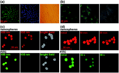 | ||
| Fig. 9 (a) Dual-color cellular imaging photos. The HEK293 cells are distinctively labeled by the bioconjugates (left: green) and Hoechst (middle: blue); right: bright field image. (b) The bioconjugates fluorescently label the cells incubated with monoclonal mouse anti-actin antibody. Left: 488 nm excitation; middle: superposition of fluorescence and transillumination images; and right: bright field image. (c) Comparison of fluorescent signals of HEK293T cells imaging with the nanospheres (top) and FITC (bottom) excited by different wavelengths. (d) Temporal evolution of fluorescence of the HEK293T cells labeled with the as-prepared nanospheres (top) and FITC (bottom). The nanospheres and FITC were both excited at 488 nm by argon laser with 8 μs dwell time and ∼15 mW power. (Parts (a) and (b) reprinted with permission from ref. 12, © 2009 American Chemical Society; parts (c) and (d) reprinted with permission from ref. 13, © 2009 Wiley.) | ||
The above reports show that the highly luminescent and stable Si dots, and especially their antibody bioconjugates, are promising fluorescent biological probes for various bioapplications, including long-term and real-time cellular labeling.12,13,16
4.2 Bio-imaging of SiNWs
Near-infrared fluorescence and spontaneous Raman scattering have been used to track carbon nanotubes in live cells and live animals.159 Further, an intrinsic multiphoton luminescence also has been used to visualize low-aspect-ratio gold nanorods and nanoshells in live cells and implanted tumors, while more than 95% of the excitation energy is actually converted into heat, causing effective phototoxicity to cells.159–166 Therefore, nanosystems with precise control of size, shape and surface chemistry, and an intense and intrinsic optical signal with low damage potential are desired. In some way, SiNWs have unparalleled dimension-control properties, which are potentially useful for the above applications.121,159,167–169Recently, Jung et al. reported strong and stable third-order nonlinear optical (NLO) signals, including four-wave mixing (FWM) and third-harmonic generation (THG), from SiNWs of diameters as small as 5 nm (see Fig. 10).159 They further employed such signals to monitor SiNWs circulating in the peripheral blood of a live mouse and to map the organ distribution of systemically administrated SiNWs. The intensive FWM and THG emissions properties open up exciting opportunities for using SiNWs as a novel in vivo imaging agent offering intrinsic 3D spatial resolution, high photostability, and orientation information. With the advantages of controllable dimensions, versatile surface chemistry, and an intensive intrinsic NLO signals, SiNWs would provide an exciting nanobio-system for investigating the cellular interaction with one-dimension nanomaterials.159
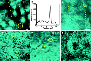 | ||
| Fig. 10 In vivo FWM images of SiNWs. (a) FWM image (red) of the peripheral blood of a living mouse taken at 20 min post injection of PEGylated SiNW PBS solution. Yellow dashed lines mark the blood vessel. The white solid line indicates the scan line for the intensity profile shown in (b). (b) FWM intensity profile from the line scan along the flowing SiNW. (c) FWM image of the peripheral blood of a living mouse taken post injection of PBS. (d–f) FWM images of SiNWs (red) deposited in the liver (d), spleen (e), and kidney (f) explanted at 1 h post injection. All FWM images are superimposed with transmission images (cyan) taken simultaneously. The SiNWs were highlighted by yellow circles. Scale bars, 5 μm. (Reprinted with permission from ref. 159, © 2009 American Chemical Society.) | ||
5. Applications in nanocatalysis and energy issue
5.1 Catalytic properties of Si dots
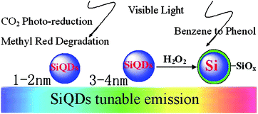
Nanocatalysis is an exciting field in nanoscience and nanochemistry. Its main objective is the design of nanocatalysts (a new-generation catalyst) with strong and tunable chemical activity, specificity, and selectivity.8,9,138,170–172 A good photocatalyst should be able to utilize visible and/or near UV light and be photo-stable (against photocorrosion), inexpensive, and non-toxic.9,138,170,171 Nanoscience research can greatly impact on the development of new and more potent catalystsvia design and control of photocatalyst properties, especially in terms of energy gap, chemical composition, and surface modification. As good photosensitizers, porous Si and Si nanoparticles are powerful for singlet oxygen generation in solution.9,172 In particular, size-controlled Si quantum dots show tunable emissions from near-infrared to blue wavelength, making them promising candidates as photocatalysts.Recently, Kang et al. demonstrated that indeed 1–2 nm Si quantum dots could function as excellent photocatalysts for CO2 reduction and dye (methyl red) degradation, while 3–4 nm Si quantum dots were effective photocatalysts for the selective oxidation of benzene (see Fig. 11).9 It suggests that Si quantum dots can be regarded as a general photocatalyst which shows the size-dependent emission and photocatalytic activity of Si quantum dots for different reactions. In sharp contrast to 1–2 nm Si quantum dots, 3–4 nm Si quantum dots showed no photochemical reduction of CO2/CO32− and little or no photodegradation of methyl red. The striking difference is attributed to the larger e−/h+ pair energy of 1–2 nm Si quantum dots than that of 3–4 nm Si quantum dots, so that the former have sufficient energy to induce photochemical reduction of CO2/CO32− and degradation of methyl red (see Fig. 12a, c and d), whereas 3–4 nm Si quantum dots would function as a photocatalyst for hydroxylation of aromatic hydrocarbons (benzene) (see Fig. 12b and e). The hydroxylation of benzene yielded almost 100% phenol and light was essential for the high selectivity, since control experiments in the dark produced less than 95% phenol and by-products from over-oxidation of phenol. During the reaction, H–Si quantum dots were partially oxidized by H2O2 and formed Si/SiOx core-shell structure.57 On the Si/SiOx surface, H2O2 molecules adsorbed and decomposed into active oxygen species with oxene characteristics, which were electrophilic and prone to oxidize benzene ring to phenol. Significantly, the products (phenols) were protected by the photoelectron reductive environment, which prevented further oxidation of phenols, thus yielding a high selectivity of phenol formation (see Fig. 12f).
 | ||
| Fig. 11 Scheme of different-diameters SiQDs for different reactions. (Reprinted with permission from ref. 9, © 2007 American Chemical Society.) | ||
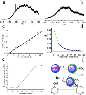 | ||
| Fig. 12 PL spectra of SiQDs for (a) 1–2 nm and (b) 3–4 nm. (c) The relationship between products (CHO/HCOOH) concentration and reaction time. (d) The relationship between methyl red concentration and reaction time. (e) The relationship between benzene conversion and reaction time with 3–4 nm SiQDs as photocatalyst. (f) The possible catalytic mechanism for benzene to phenol. (Reprinted with permission from ref. 9, © 2007 American Chemical Society). | ||
Such capabilities of Si quantum dots are attributable to their tunable band gap and excellent photoconductivity properties. By controlling the surface and band gap of Si quantum dots, one can expect to design and prepare more novel catalystsvia modification with different nano-species (e.g.TiO2, Au, Pt, C, etc.).9,57
5.2 Catalysis of SiNWs
Nanosized gold (Au) and copper (Cu) particles have attracted much attention due to their exceptional potential for catalyzing selective epoxidation reactions.2a,b On the other hand, nanostructured Si (porous Si and Si nanoparticles) are good photosensitizers for singlet oxygen generation,9,171 while Si quantum dots show high selectivity in photo-assisted oxidation of aromatic hydrocarbons.9 In light of the respective merits of metal and Si nanostructures, SiNWs coated with metal (Au, Cu, Ag, Pt, Pdet al.) nanoparticles may exhibit enhanced catalytic properties. Lee and coworkers demonstrated the excellent catalytic activity of Au nanoparticles-modified Si nanowires (AuNPs/SiNWs) and Cu nanoparticles-modified SiNWs (CuNPs/SiNWs) for selective oxidation of cis-cyclooctene at 60–80 °C in ambient air, in the absence of solvent and oxidant (see Fig. 13).138 Single crystalline AuNPs and CuNPs deposited on SiNWs would provide large surface area and act as a potential material for preparation of novel catalyst. Specifically, the conversion of cis-cyclooctene up to 38.3% and 28.3% was achieved by using AuNPs/SiNWs and CuNPs/SiNWs as catalysts, respectively, and the corresponding selectivity to the epoxide is 90% and 97.6%. The reaction pathway of the metal-modified SiNWs system is possibly similar to that of the Au/C catalyst system, in that TBHP acts as a free radical initiator with oxygen in air as the oxidant,138,171 while the CC bond is directly oxidized by a peroxide species generated from TBHP and oxygen.138,171 In comparison to carbon, SiNWs as a substrate substantively enhanced the catalytic ability (selectivity and conversion) of the supported metals. Besides the large surface area, the highly reactive nature of metal-modified SiNWs is associated with the unique ability of H-SiNWs (SiNWs after HF-treatment) in anchoring metal NPs (e.g.Au, Cu, Ag, Pt, etc.) firmly and separately on SiNWs surfaces. These findings not only show that metal (Au, Cu)-modified SiNWs are superior catalysts for selective oxidation of hydrocarbons, but also that SiNWs are a powerful substrate support (enhancing efficiency and selectivity) for nanocatalysts.138
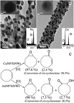 | ||
| Fig. 13 TEM images of Au/SiNWs (a) and Cu/SiNWs (b). HRTEM images are in upper insets and EDX spectra in lower insets. (c) Reaction schemes of cis-cyclooctene epoxidation catalyzed by Cu- and Au-modified SiNWs at 60–80 °C for 24 h. (Reprinted with permission fromref. 138, © 2009 The Royal Society of Chemistry.) | ||
Further, Shao and coworkers showed that Au–Pd bimetallic nanoparticles on SiNWs can be used as a photocatalyst for p-nitroaniline decomposition.173 The results obviously indicate that the catalytic activity and stability of Au–Pd/Si catalysts are promising, and the addition of Au to Pd enhances the catalytic activity. The Au–Pd bimetallic system was prepared using SiNW as a carrier; it has a high surface area making it an attractive host to support nanoparticles. The SiNW-supported Au–Pd catalysts provided higher catalytic activity in the reduction of p-nitroaniline than the Pd/Si or Au/Si catalysts. Experiments also confirmed that metal-modified SiNWs have excellent photocatalytic abilities for dye decomposition.
The photo-active surface of SiNWs also exhibited a highly selective catalytic oxidation of benzene to phenol in the presence of H2O2.138 The high selectivity was attributed to the synergy of active oxygen species oxidation and photo-induced electron reduction. The possible pathway for this reaction is assisted by the participation of the active oxygen species. Active oxygen species were produced by the interaction of active surface of Si/SiOx core–shell structure and visible light. As active oxygen species selectively attack the benzene ringviahydroxylation, electrophilic oxygen species should be responsible for the oxidation of benzene. The performance H-SiNWs throughout the hydroxylation of benzene was similar to that of H–Si quantum dots in the same reaction.
HF-treated SiNWs (H-SiNWs) can also serve as catalysts in the degradation of rhodamine B, as well as oxidization of benzyl alcohol to benzoic acid.174 H-SiNWs exhibit a better photocatalytic activity than Pd-, Au-, Rh-, or Ag-modified SiNWs in the degradation of rhodamine B (see Fig. 14). The photocatalytic activity of metal-semiconductor catalysts depends largely on the electron work function of metals, which is a key parameter in the electron transfer process from conducting band to metal.174 Significantly, H-terminated SiNWs surfaces also play a key factor for the high photocatalytic ability of SiNWs. On the surface of H-SiNWs, there are monohydride (SiH), dihydride (SiH2), and trihydride (SiH3) species, which are electron-deficient and may serve as an electron sinks, thus enhancing the oxidizing ability.174
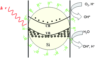 | ||
| Fig. 14 Schematic of the electron–hole generation in H-SiNW photocatalyst and the mechanisms involved: (left) light promotes the formation of the electron and hole; (middle) the electron transfer to hydrogen atom on the surface; (right) the hole is used in the formation of the OH* groups promoting oxidising processes. (Reprinted with permission from ref. 174, © 2009 American Chemical Society.) | ||
Yang et al. reported on the catalyst design based on SiNWs and TiO2 complex structures.175TiO2 has been extensively studied as a photoanode due to its high resistance to photocorrosion.175–181 However, the conversion efficiency of solar energy in water splitting to hydrogen is still low due to the large band gap and chemical over potential of TiO2.175–177,182Si can absorb sunlight efficiently but, however, may not be useful for photoelectrolysis since it readily corrodes in water. Moreover, it is thermodynamically impossible for Si to oxidize water spontaneously due to its high valence band maximum (VBM) energy. Therefore, a composite semiconductor electrode composed of a semiconductor heterojunction has been proposed to overcome these shortcomings.175 Yang et al. compared the photocurrent density of the planar Si and SiNWs coated by TiO2 thin film. The SiNW/TiO2 has a photocurrent density 2.5 times higher than the planar Si/TiO2 due to a lower light reflectance and a higher surface area. They also observed an increase of the photocurrent by using n-Si/n-TiO2 heterojunctions because n/n junctions enhance the charge separation and minimize recombination. The n/n heterojunction is a promising structure for solar water splitting since the photovoltage at the junction can compensate for the lower energy level of the conduction band of the shell semiconductor. Also, the n/n heterojunction could potentially increase the efficiency of the photovoltaic cell due to a higher open circuit voltage and higher photocurrent.175
5.3 Applications in energy
For thermoelectric applications, Yang et al. have measured the thermal conductivities of SiNWs of different diameters (22, 37, 56, and 115 nm).183 The thermal conductivities of SiNWs are about two orders of magnitude lower than that of the bulk Si. As the diameter of SiNWs decreased, the corresponding thermal conductivity reduced. This result indicates that enhanced boundary scattering has a strong effect on the phonon transport in SiNWs. SiNWs arrays show promise as high-performance, scalable thermoelectric materials. Further, these results suggest the high potential of SiNWs for thermoelectric applications in waste heat salvaging, power generation, and solid-state refrigeration.For lithium battery applications, Cui et al. reported that SiNW battery electrodes exhibited the theoretical Li charge capacity for Si anodes and maintained a discharge capacity close to 75% of this maximum, with little fading during cycling.184 First, SiNWs with small diameters allow a better accommodation of the large volume changes without the initiation of fracture that usually occurs in bulk or micron-sized materials. Second, each SiNW is electrically connected to the metallic current collector so that all the nanowires contribute to the charge capacity. Third, SiNWs have direct 1D electronic pathways allowing for efficient charge transport. In the electrode microstructures based on particles, electronic charge carriers must move through small interparticle contact areas. In addition, as every SiNW is connected to the current-carrying electrode, the need for binders or conducting additives of extra weight is eliminated. Recently, Cui et al. further developed similar Si nanostructures as battery electrodes, such as Si core–shell structure and Si nanotubes, and checked their electrochemistry abilities.185–187 The results show the high capacity of Si nanostructures at high rate charging and discharging.185–189
For solar cell applications, SiNWs have naturally become the focus of photovoltaic research since they may be readily compatible with the existing Si industry and processing technology.190–198 Lieber et al. have reported coaxial core–shell SiNWs as building blocks for photovoltaic devices, and single coaxial SiNWs solar cells with short-circuit current densities (Jsc) reaching 23.9 mA cm−2 and power conversion efficiencies of 3.4% under solar equivalent illumination.192 They also fabricated axial modulation-doped p-i-n and tandem p-i-n+–p+-i-n SiNW photovoltaic elements.196 Recent reports showed that highly-oriented SiNWs arrays prepared by the electroless etching method can significantly suppress light reflection across a broad spectrum and serve as an antireflection coating for Si solar cell applications.190,199–201 Sivakov et al. fabricated SiNWs-based solar cells on glass substrates by electroless etching, yielding a maximum power conversion efficiency of 4.4%.202 Recent studies of photoelectrochemical (PEC) solar cells have shown SiNWs to be rather photoactive, revealing the high potential of SiNWs for inexpensive PEC cells.190,203–205 Notably, Lee et al. prepared platinum nanoparticle (PtNP)-decorated SiNWs arrays and evaluated their potential application for solar energy conversion. PtNP-decorated SiNW arrays yielded significant enhancement in solar energy conversion efficiency up to 8.1%, demonstrating them to be a promising hybrid system for efficient solar energy conversion. The PtNP–Si junctions and the excellent catalytic activity of PtNPs for the electrode processes are considered responsible for enhancing the solar energy conversion efficiency of PtNP-decorated SiNWs arrays.190
6. Summary and outlook
In this review, we describe the recent advances in the research on small-sized Si NPs, focusing on their synthesis and surface functionalization, photoluminescence properties, applications in bio-imaging, and nanocatalysts and energy issues. There are a variety of synthesis techniques for SS SiNPs of different characteristics; e.g. chemical and electrochemical methods are attractive in producing Si dots with high-reactivity surfaces (Si–H, Si–OH, and Si–C bond) for easy functionalization, while physical methods are preferred for production of high-quality electronic-grade SiNWs. The PL and optical properties of SS SiNPs are interesting and intriguing, constituting a rich and hot research topic, but their origins remain unclear. The promising potential of SS SiNPs for bioapplications is due to the following characteristics: (i) they are strongly emitting, tunable in emission wavelength, photostable, and pH stable; and (ii) they have a robust and flexible surface chemistry that facilitates water dispersibility and easy conjugation of DNA or protein probes. To realize biochemical utility, it is necessary to produce SS SiNPs of controlled sizes with appropriate biochemical functionalities (e.g.DNA/PNA probes and antibodies). While Si is generally considered to be biocompatible, the cytotoxicity properties of SS Si NPs need to be critically assessed and confirmed. The unique bipolar electron donating–accepting ability as well as excellent light harvesting capability make SS Si NPs an exceptional candidate for catalyst, battery and photovoltaic applications. By modification of surface and band gap via functionalization, we can expect to design novel catalysts from SS Si NPs for green chemistry, and new energy issues. The rich PL and optical properties, excellent bioprobe characteristics (small-sized, strongly emitting, water dispersible, biocompatible, pH and photostable), and distinctive transport and electrical properties offer many unique opportunities to develop SS Si NPs for myriad exciting applications in bio-imaging, nanocatalysis and new energy.Acknowledgements
This work is supported by the National Basic Research Program of China (973 Program) (No. 2010CB934500 and 2006CB933000), National Natural Science Foundation of China (NSFC) (No. 21073127, 21071104, 20801010 and 20803008), a Foundation for the Author of National Excellent Doctoral Dissertation of P. R. China (FANEDD) (No. 200929), and the Research Grants Council of the Hong Kong (Project No.: CityU5/CRF/08, 9041313, 9041538 & 9041476).References
- D. De Cogan, Properties of Silicon, INSPEC, London, 1988 Search PubMed.
- V. Kumar, Nanosilicon, Elsevier Ltd, 2007 Search PubMed.
- Silicon Photonics, G. T. Reed, A. P. Knights, John Wiley & Sons, Ltd, 2004, Chapter 6: A Selection of Photonic Devices (pp. 145–190); and Chapter 8: Prospects for Silicon Light-Emitting Devices (pp. 223–250).
- D. J. Lockwood, Spectroscopy of Emerging Materials, 2004, 165, 97 Search PubMed.
- A. Morales and C. M. Lieber, Science, 1998, 279, 208 CrossRef CAS; R. S. Wagner and W. C. Ellis, Appl. Phys. Lett., 1964, 4, 89 CAS; R. G. Treuting and S. M. Arnold, Acta Metall., 1957, 5, 598 CrossRef CAS; Y. F. Zhang, Y. H. Tang, N. Wang, D. P. Yu, C. S. Lee, I. Bello and S. T. Lee, Appl. Phys. Lett., 1998, 72, 1835 CrossRef CAS; H. Y. Peng, Z. W. Pan, L. Xu, X. H. Fan, N. Wang, C. S. Lee and S. T. Lee, Adv. Mater., 2001, 13, 317 CrossRef CAS.
- D. D. D. Ma, C. S. Lee, F. C. K. Au, D. S. Y. Tong and S. T. Lee, Science, 2003, 299, 1874 CrossRef CAS.
- B. K. Teo and X. H. Sun, Chem. Rev., 2007, 107, 1454 CrossRef CAS.
- Z. H. Kang, C. H. A. Tsang, Z. D. Zhang, M. L. Zhang, N. B. Wong, J. A. Zapien, Y. Y. Shan and S. T. Lee, J. Am. Chem. Soc., 2007, 129, 5326 CrossRef.
- Z. H. Kang, C. H. A. Tsang, N. B. Wong, Z. D. Zhang and S. T. Lee, J. Am. Chem. Soc., 2007, 129, 12090 CrossRef CAS.
- Y. Cui, Q. Q. Wei, H. K. Park and C. M. Lieber, Science, 2001, 293, 1289 CrossRef CAS.
- J. Zhu, H. L. Peng, A. F. Marshall, D. M. Barnett, W. D. Nix and Y. Cui, Nat. Nanotechnol., 2008, 3, 477 CrossRef CAS.
- Y. He, Y. Y. Su, X. B. Yang, Z. H. Kang, T. T. Xu, R. Q. Zhang, C. H. Fan and S. T. Lee, J. Am. Chem. Soc., 2009, 131, 4434 CrossRef CAS.
- Y. He, Z. H. Kang, Q. S. Li, C. H. A. Tsang, C. H. Fan and S. T. Lee, Angew. Chem., Int. Ed., 2009, 48, 128 CrossRef CAS.
- N. Wang, Y. F. Zhang, Y. H. Tang, C. S. Lee and S. T. Lee, Phys. Rev. B: Condens. Matter Mater. Phys., 1998, 58, R16024 CrossRef CAS; S. T. Lee, Y. F. Zhang, N. Wang, Y. H. Tang, I. Bello, C. S. Lee and Y. W. Chung, J. Mater. Res., 1999, 14, 4503 CAS; S. T. Lee, N. Wang and C. S. Lee, Mater. Sci. Eng., A, 2000, 286, 16 CrossRef; S. T. Lee, N. Wang, Y. F. Zhang and Y. H. Tang, MRS Bull., 1999, 24, 36 CAS; V. Schmidt, J. V. Wittemann and U. Gösele, Chem. Rev., 2010, 110, 361 CrossRef CAS.
- R. Q. Zhang, Y. Lifshitz and S. T. Lee, Adv. Mater., 2003, 15, 635 CrossRef CAS; C. P. Li, C. S. Lee, X. L. Ma, N. Wang, R. Q. Zhang and S. T. Lee, Adv. Mater., 2003, 15, 607 CrossRef CAS; R. Q. Zhang, T. S. Chu, H. F. Chaeung, N. Wang and S. T. Lee, Phys. Rev. B, 2001, 64, 31; T. S. Chu, R. Q. Zhang and H. F. Chaeung, J. Phys. Chem. B, 2001, 105, 1705 CrossRef CAS; V. Schmidt, J. V. Wittemann, S. Senz and U. Gösele, Adv. Mater., 2009, 21, 2681 CrossRef CAS.
- N. O'Farrell, A. Houlton and B. R. Horrocks, Int. J. Nanomed., 2006, 1, 451 CrossRef CAS.
- Z. C. Feng and R. Tsu, Porous Silicon, World Scientific, Singapore, 1994 Search PubMed.
- J. C. Vial and J. Derrien, Porous Silicon Science and Technology, Springer-Verlag, Berlin, 1995 Search PubMed.
- R. Hérino and W. Lang, Porous Silicon and Related Materials, Elsevier, Amsterdam, 1995 Search PubMed.
- P. M. Fauchet, in Light Emission in Silicon, ed. D. J. Lockwood, Academic Press, San Diego, 1997, ch. 6 Search PubMed.
- M. Jr.Bruchez, M. Moronne, P. Gin, S. Weiss and A. P. Alivisatos, Science, 1998, 281, 2013 CrossRef CAS.
- J. D. Holmes, K. J. Ziegler, R. C. Doty, L. E. Pell, K. P. Johnston and B. A. Korgel, J. Am. Chem. Soc., 2001, 123, 3743 CrossRef CAS.
- W. L. Wilson, P. F. Szajowski and L. E. Brus, Science, 1993, 262, 1242 CAS.
- S. S. Iyer and Y.-H. Xie, Science, 1993, 260, 40 CrossRef CAS.
- S. H. Risbud, L.-C. Liu and J. F. Shackelford, Appl. Phys. Lett., 1993, 63, 1648 CrossRef CAS.
- M. Fujii, S. Hayashi and K. Yamamoto, Jpn. J. Appl. Phys., 1991, 30, 687 CrossRef CAS.
- J. G. Zhu, C. W. White, J. D. Budal, S. P. Withrow and Y. Chen, J. Appl. Phys., 1995, 78, 4386 CrossRef CAS.
- W. A. Saunders, P. C. Sercel, R. B. Lee, H. A. Atwater, K. J. Vahala, R. C. Flagan and E. J. Escorcia-Aparcio, Appl. Phys. Lett., 1993, 63, 1549 CrossRef CAS.
- T. Yoshida, T. Takeyama, Y. Yamada and K. Mutoh, Appl. Phys. Lett., 1996, 68, 1772 CrossRef CAS.
- L. Pavasi, L. Del Negro, C. Mazzoleni, G. Franzo and F. Priolo, Nature, 2000, 408, 440 CrossRef CAS; A. Borgensi, A. Sasella, B. Pivas and L. Pavesi, Solid State Commun., 1993, 87, 1 CrossRef.
- A. Fojtik, H. Weller, S. Fiechter and A. Henglein, Chem. Phys. Lett., 1987, 134, 477 CrossRef CAS.
- A. Fojtik and A. Henglein, Chem. Phys. Lett., 1994, 221, 363 CrossRef CAS.
- J. J. Wu and R. C. Flagan, J. Appl. Phys., 1993, 73, 407 CrossRef.
- H. Takagi, H. Ogawa, Y. Yamazaki, A. Ishizaki and T. Nakagiri, Appl. Phys. Lett., 1990, 56, 2379 CrossRef CAS.
- R. Okada and S. Iijima, Appl. Phys. Lett., 1991, 58, 1662 CrossRef CAS.
- D. J. DiMaria, J. R. Kirtley, E. J. Pakulis, D. W. Dong, T. S. Kuan and F. L. Pesavento, J. Appl. Phys., 1984, 56, 401 CrossRef CAS.
- S. Berger, L. Schächter and S. Tamir, Nanostruct. Mater., 1997, 8, 231 CrossRef CAS.
- B. D. Rowsell and J. G. C. Veinot, Nanotechnology, 2005, 16, 732 CrossRef CAS; J. R. Heath, J. J. Shiang and A. P. Alivisatos, J. Chem. Phys., 1994, 101, 1607 CrossRef CAS; A. Kornowski, M. Giersig, R. Vogel, A. Chemseddine and H. Weller, Adv. Mater., 1993, 5, 634 CrossRef CAS.
- D. Mayeri, B. L. Phillips, M. P. Augustine and S. M. Kauzlarich, Chem. Mater., 2001, 13, 765 CrossRef CAS.
- R. K. Baldwin, K. A. Pettigrew, E. Ratai, M. P. Augustine and S. M. Kauzlarich, Chem. Commun., 2002, 1822 RSC.
- J. Zou, R. K. Baldwin, K. A. Pettigrew and S. M. Kauzlarich, Nano Lett., 2004, 4, 1181 CrossRef CAS.
- J. P. Wilcoxon, G. A. Samara and P. N. Provencio, Phys. Rev. B: Condens. Matter Mater. Phys., 1999, 60, 2704 CrossRef CAS.
- Y. H. Xie, W. L. Wilson, F. M. Ross, J. A. Mucha, E. A. Fitzgerald, J. M. Macaulay and T. D. Harris, Appl. Phys. Lett., 1992, 71, 2403 CAS.
- R. C. Anderson, R. S. Muller and C. W. Tobias, J. Electrochem. Soc., 1993, 140, 1393 CAS.
- A. Grosman and C. Ortega, Properties of Porous Silicon, Ed. L. T. Canham, INSPEC, London, 1997, p. 145 Search PubMed; R. A. Bley, S. M. Kauzlarich, J. E. Davis and H. W. Lee, Chem. Mater., 1996, 8, 1881 Search PubMed.
- J. L. Heinrich, C. L. Curtis, G. M. Credo, K. L. Kavanagh and M. J. Saylor, Science, 1992, 255, 66 CrossRef CAS.
- G. Belomoin, J. Therrien, A. Smith, S. Rao, R. Twesten, S. Chaieb, M. H. Nayfeh, L. Wagner and L. Mitas, Appl. Phys. Lett., 2002, 80, 841 CrossRef CAS.
- W. Brown, R. Freeman, K. Raghavachari and M. Schulter, Science, 1987, 235, 860 CrossRef CAS; L. Bloomfield, R. Freeman and W. Brown, Phys. Rev. Lett., 1985, 54, 2246 CrossRef CAS.
- K. Raghavachari, Phase Transit., 1990, 24–26, 61 CrossRef CAS.
- U. Rothlisberger, W. Andreoni and M. Parrinello, Phys. Rev. Lett., 1994, 72, 665 CrossRef; W. Andreoni and G. Pastore, Phys. Rev. B: Condens. Matter, 1990, 41, 10243 CrossRef CAS; U. Rothlisberger, W. Andreoni and P. Ginnozzi, J. Chem. Phys., 1992, 96, 1248 CrossRef.
- L. Anderson, S. Muruyama and R. Smalley, Chem. Phys. Lett., 1991, 176, 348 CrossRef CAS; H. Kroto, J. Heath, S. O'Brian, R. Curl and R. Smalley, Nature, 1985, 318, 162 CrossRef CAS.
- Z. H. Kang, E. B. Wang, B. D. Mao, Z. M. Su, L. Gao, S. Y. Lian and L. Xu, J. Am. Chem. Soc., 2005, 127, 6534 CrossRef CAS.
- B. Vigolo, A. Pénicaud, C. Coulon, C. Sauder, R. Pailler, C. Journet, P. Bernier and P. Poulin, Science, 2000, 290, 1331 CrossRef CAS.
- A. Muller, F. Petters, M. T. Pope and D. Gatteschi, Chem. Rev., 1998, 98, 239 CrossRef.
- J. T. Rhule, C. L. Hill, D. A. Judd and R. F. Schinazi, Chem. Rev., 1998, 98, 327 CrossRef CAS.
- W. B. Kim, T. Voitl, G. J. Rodriguez-Rivera and J. A. Dumesic, Science, 2004, 305, 1280 CrossRef CAS.
- Z. H. Kang, Y. Liu, C. H. A. Tsang, D. D. D. Ma, X. Fan, N. B. Wong and S. T. Lee, Adv. Mater., 2009, 21, 661 CrossRef CAS.
- T. E. Olinga, J. Frayasse, J. P. Travers, A. Dufresne and A. Pron, Macromolecules, 2000, 33, 2107 CrossRef CAS.
- J. Frayasse, J. Planes, A. Dufresne and A. Guermache, Macromolecules, 2001, 34, 8143 CrossRef.
- D. Stauffer, Introduction to Percolation Theory, Taylor and Francis, Philadelphia, 1985 Search PubMed.
- S. Kodambaka, J. Tersoff, M. C. Reuter and F. M. Ross, Phys. Rev. Lett., 2006, 96, 096105 CrossRef CAS.
- V. A. Nebol'sin, A. A. Shchetinin, A. A. Dolgachev and V. V. Korneeva, Inorg. Mater., 2005, 41, 1256 CrossRef CAS.
- Y. Wang, V. Schmidt, S. Senz and U. Gösele, Nat. Nanotechnol., 2006, 1, 186 CrossRef CAS.
- S. Hofmann, R. Sharma, C. T. Wirth, F. Cervantes-Sodi, C. Ducati, T. Kasama, R. E. Dunin-Borkowski, J. Drucker, P. Bennett and J. Robertson, Nat. Mater., 2008, 7, 372 CrossRef CAS.
- S. Hofmann, C. Ducati, R. J. Neill, S. Piscanec, A. C. Ferrari, J. Geng, R. E. Dunin-Borkowski and J. Robertson, J. Appl. Phys., 2003, 94, 6005 CrossRef CAS.
- S. Sharma and M. K. Sunkara, Nanotechnology, 2004, 15, 130 CrossRef.
- F. Iacopi, P. M. Vereecken, M. Schaekers, M. Caymax, N. Moelans, B. Blanpain, O. Richard, C. Detavernier and H. Griffiths, Nanotechnology, 2007, 18, 505307 CrossRef.
- A. V. Sandulova, P. S. Bogoyavlenskii and M. I. Dronyum, Sov. Phys. Solid State, 1964, 5, 1883.
- R. S. Wagner, W. C. Ellis, K. A. Jackson and S. M. Arnold, J. Appl. Phys., 1964, 35, 2993 CAS.
- E. S. Greiner, J. A. Gutowski and W. C. Ellis, J. Appl. Phys., 1961, 32, 2489 CrossRef CAS.
- T. R. Hogness, T. L. Wilson and W. C. Johnson, J. Am. Chem. Soc., 1936, 58, 108 CrossRef CAS.
- H. Schäfer and B. Morcher, Z. Anorg. Allg. Chem., 1957, 290, 279 CrossRef CAS.
- H. Nagayoshi, H. Nordmark, R. Holmestad, N. Matsumoto, S. Nishimura, K. Terashima, J. C. Walmsley and A. Ulyashin, Jpn. J. Appl. Phys., 2008, 47, 4807 CrossRef CAS.
- J. B. Hannon, S. Kodambaka, F. M. Ross and R. M. Tromp, Nature, 2006, 440, 69 CrossRef CAS.
- F. M. Ross, J. Tersoff and M. C. Reuter, Phys. Rev. Lett., 2005, 95, 146104 CrossRef CAS.
- S. Kodambaka, J. B. Hannon, R. M. Tromp and F. M. Ross, Nano Lett., 2006, 6, 1292 CrossRef CAS.
- Y. Cui, L. H. Lauhon, M. S. Gudiksen, J. Wang and C. M. Lieber, Appl. Phys. Lett., 2001, 78, 2214 CrossRef CAS.
- W. I. Park, G. Zheng, X. Jiang, B. Tian and C. M. Lieber, Nano Lett., 2008, 8, 3004 CrossRef CAS.
- Y. F. Wang, K. K. Lew, T. T. Ho, S. W. Pan, L. Novak, E. C. Dickey, T. S. Redewing and J. M. Mayer, Nano Lett., 2005, 5, 2139 CrossRef CAS.
- L. Pan, K. K. Lew, J. M. Redwing and C. Dickey, J. Cryst. Growth, 2005, 277, 428 CrossRef CAS.
- H. Schmid, M. T. Bjork, J. Knoch, H. Riel and W. Riess, J. Appl. Phys., 2008, 103, 024304 CrossRef.
- C. Mouchet, L. Latu-Romain, C. Cayron, E. Rouviere, C. Celle and J. P. Simonato, Nanotechnology, 2008, 19, 335603 CrossRef.
- V. Schmidt, S. Senz and U. Gösele, Nano Lett., 2005, 5, 931 CrossRef CAS.
- X. Y. Zhang, L. D. Zhang, G. W. Meng, G. H. Li, N. Y. Jin-Phillipp and F. Phillipp, Adv. Mater., 2001, 13, 1238 CrossRef CAS.
- K. K. Lew, C. Reuther, A. H. Carim, J. M. Redwing and B. R. Martin, J. Vac. Sci. Technol., B, 2002, 20, 389 CrossRef CAS.
- T. Shimizu, T. Xie, J. Nishikawa, S. Shingubara, S. Senz and U. Gösele, Adv. Mater., 2007, 19, 917 CrossRef CAS.
- Z. W. Pan and Z. R. Dai, J. Phys. Chem. B, 2001, 105, 2507 CrossRef CAS.
- Q. Gu, H. Dang, J. Cao, J. Zhao and S. Fan, Appl. Phys. Lett., 2000, 76, 3020 CrossRef CAS.
- F. M. Kolb, H. Hofmeister, R. Scholz, M. Zacharias, U. Gösele, D. D. Ma and S. T. Lee, J. Electrochem. Soc., 2004, 151, G472 CrossRef CAS.
- N. Wang, Y. H. Tang, Y. F. Zhang, D. P. Yu, C. S. Lee, I. Bello and S. T. Lee, Chem. Phys. Lett., 1998, 283, 368 CrossRef CAS.
- N. Wang, Y. H. Tang, Y. F. Zhang, C. S. Lee, I. Bello and S. T. Lee, Chem. Phys. Lett., 1999, 299, 237 CrossRef CAS.
- P. Werner, N. D. Zakharov, G. Gerth, L. Schubert and U. Gösele, Int. J. Mater. Res., 2006, 97, 1008 Search PubMed.
- P. D. Kanungo, N. Zakharov, J. Bauer, O. Breitenstein, P. Werner and U. Gösele, Appl. Phys. Lett., 2008, 92, 263107 CrossRef.
- N. D. Zakharov, P. Werner, G. Gerth, L. Schubert, L. Sokolov and U. Gösele, J. Cryst. Growth, 2006, 290, 6 CrossRef CAS.
- L. Schubert, P. Werner, N. D. Zakharov, G. Gerth, F. M. Kolb, L. Long, U. Gösele and T. Y. Tan, Appl. Phys. Lett., 2004, 84, 4968 CrossRef CAS.
- Y. F. Zhang, Y. F. Tang, N. Wang, C. S. Lee, I. Bello and S. T. Lee, Appl. Phys. Lett., 1998, 72, 1835 CrossRef CAS.
- G. W. Zhou, Z. Zhang, Z. G. Bai, S. Q. Feng and D. P. Yu, Appl. Phys. Lett., 1998, 73, 677 CrossRef.
- Y. H. Yang, S. J. Wu, H. S. Chiu, P. I. Lin and Y. T. Chen, J. Phys. Chem. B, 2004, 108, 846 CrossRef CAS.
- Y. F. Zhang, Y. H. Tang, H. Y. Peng, N. Wang, C. S. Lee, I. Bello and S. T. Lee, Appl. Phys. Lett., 1999, 75, 1842 CrossRef CAS.
- J. D. Holmes, K. P. Johnston, R. C. Doty and B. A. Korgel, Science, 2000, 287, 1471 CrossRef CAS.
- X. M. Lu, T. Hanrath, K. P. Johnston and B. A. Korgel, Nano Lett., 2003, 3, 93 CrossRef CAS.
- T. Hanrath and B. A. Korgel, Adv. Mater., 2003, 15, 437 CrossRef CAS.
- H. Y. Tuan, A. Ghezelbash and B. A. Korgel, Chem. Mater., 2008, 20, 2306 CrossRef CAS.
- A. T. Heitsch, D. D. Fanfair, H. Y. Tuan and B. A. Korgel, J. Am. Chem. Soc., 2008, 130, 5436 CrossRef CAS.
- T. Tezuka, E. Toyoda, S. Nakaharai, N. T. N. Hirashita, N. Sugiyama, Y. Yamashita, O. Kiso, M. Harada, T. Yamamoto and S. Takagi, IEDM Tech. Dig., 2007, 887 Search PubMed.
- S. F. Feste, J. Knoch, D. Buca and S. Mantl, Thin Solid Films, 2008, 517, 320 CrossRef CAS.
- K. N. Lee, S. W. Jung, K. S. Shin, W. H. Kim, M. H. Lee and W. K. Seong, Small, 2008, 4, 642 CrossRef CAS.
- S. D. Suk, S. Y. Lee, S. M. Kim, E. J. Yoon, M. S. Kim, M. Li, C. W. Oh, K. H. Yeo, S. H. Kim, D. S. Shin, K. H. Lee, H. S. Park, J. N. Han, C. J. Park, J. B. Park, D. W. Kim, D. Park and B. Ryu, IEDM Tech. Dig., 2005, 717 Search PubMed.
- S. D. Suk, K. H. Yeo, K. H. Cho, M. Li, Y. Y. Yeoh, S.-Y. Lee, S. M. Kim, E. J. Yoon, M. S. Kim, C. W. Oh, S. H. Kim, D.-W. Kim and D. Park, IEEE Trans. Nanotechnol., 2008, 7, 181 CrossRef.
- N. Singh, K. D. Buddharaju, S. K. Manhas, A. Agarwal, S. C. Rustagi, G. C. Lo, N. Balasubramanian and D.-L. Kwong, IEEE Trans. Electron Devices, 2008, 55, 3107 CrossRef CAS.
- J. R. Heath, Acc. Chem. Res., 2008, 41, 1609 CrossRef CAS.
- H. I. Liu, D. K. Biegelsen, N. M. Johnson, F. A. Ponce and R. F. W. Pease, J. Vac. Sci. Technol., B, 1993, 11, 2532 CrossRef CAS.
- C.-M. Hsu, S. T. Connor, M. X. Tang and Y. Cui, Appl. Phys. Lett., 2008, 93, 133109 CrossRef.
- K. J. Morton, G. Nieberg, S. Bai and S. Y. Chou, Nanotechnology, 2008, 19, 345301 CrossRef.
- D. Zschech, D. H. Kim, A. P. Milenin, R. Scholz, R. Hillebrand, C. J. Hawker, T. P. Russell, M. Steinhart and U. Gösele, Nano Lett., 2007, 7, 1516 CrossRef CAS.
- K. Q. Peng, Y. J. Yan, S. P. Gao and J. Zhu, Adv. Mater., 2002, 14, 1164 CrossRef CAS; M. L. Zhang, K. Q. Peng, X. Fan, J. S. Jie, R. Q. Zhang, S. T. Lee and N. B. Wong, J. Phys. Chem. C, 2008, 112, 4444 CrossRef CAS; K. Q. Peng, J. J. Hu, Y. J. Yan, Y. Wu, H. Fang, Y. Xu, S. T. Lee and J. Zhu, Adv. Funct. Mater., 2006, 16, 387 CrossRef CAS.
- K. Peng, Z. Huang and J. Zhu, Adv. Mater., 2004, 16, 73 CrossRef CAS; K. Q. Peng, M. L. Zhang, A. J. Lu, N. B. Wong, R. Q. Zhang and S. T. Lee, Appl. Phys. Lett., 2007, 90, 163123 CrossRef; K. Q. Peng, H. Fang, J. J. Hu, Y. Wu, J. Zhu, Y. J. Yan and S. T. Lee, Chem.–Eur. J., 2006, 12, 7942 CrossRef CAS; K. Q. Peng, A. J. Lu, R. Q. Zhang and S. T. Lee, Adv. Funct. Mater., 2008, 19, 3026 CrossRef.
- A. I. Hochbaum, R. Chen, R. D. Delgado, W. Liang, E. C. Garnett, M. Najarian, A. Majumdar and P. Yang, Nature, 2008, 451, 163 CrossRef CAS.
- Z. Huang, H. Fang and J. Zhu, Adv. Mater., 2007, 19, 744 CrossRef CAS.
- Z. Huang, X. Zhang, M. Reiche, L. Liu, W. Lee, T. Shimizu, S. Senz and U. Gösele, Nano Lett., 2008, 8, 3046 CrossRef CAS.
- B. K. Teo, C. P. Li, X. H. Sun, N. B. Wong and S. T. Lee, Inorg. Chem., 2003, 42, 6723 CrossRef CAS; N. R. B. Coleman, M. A. Morris, T. R. Spalding and J. D. Holmes, J. Am. Chem. Soc., 2001, 123, 187 CrossRef CAS; N. R. B. Coleman, N. O'Sullivan, K. M. Ryan, T. A. Crowley, M. A. Morris, T. R. Spalding, D. C. Steytler and J. D. Holmes, J. Am. Chem. Soc., 2001, 123, 7010 CrossRef CAS; C. P. Li, X. H. Sun, N. B. Wong, C. S. Lee, S. T. Lee and B. K. Teo, Chem. Phys. Lett., 2002, 365, 22 CrossRef CAS.
- O. Akcakir, J. Therrien, G. Belomoin, N. Barry, E. Gratton and M. Nayfeh, Appl. Phys. Lett., 2000, 76, 1857 CrossRef CAS.
- G. Belomoin, J. Therrien and M. Nayfeh, Appl. Phys. Lett., 2000, 77, 779 CrossRef CAS.
- M. Nayfeh, N. Rigakis and Z. Yamani, Phys. Rev. B: Condens. Matter, 1997, 56, 2079 CrossRef CAS; MRS, 1998, 486, p. 243 Search PubMed.
- G. Allan, C. Delerue and M. Lannoo, Phys. Rev. Lett., 1996, 76, 2961 CrossRef CAS.
- S. Nakagomi, K. Muto and M. Itoh, Sens. Actuators, B, 2001, 72, 108 CrossRef; T. J. Fawcett, J. T. Wolan, R. L. Myers, J. Walker and S. E. Saddow, Appl. Phys. Lett., 2004, 85, 416 CrossRef CAS; S. Maekawa, J. Tamaki, N. Miura and N. Yamazoe, Sens. Actuators, B, 1992, 9, 71 CrossRef; J. Mizsei, Sens. Actuators, B, 1995, 28, 129 CrossRef.
- J. M. Buriak, Chem. Rev., 2002, 102, 1271 CrossRef CAS; D. D. M. Wayner and R. A. Wolkow, J. Chem. Soc., Perkin Trans., 2002, 2, 23 Search PubMed.
- A. Bansal, X. Li, I. Lauermann, N. S. Lewis, S. I. Yi and W. H. Weinberg, J. Am. Chem. Soc., 1996, 118, 7225 CrossRef CAS; T. Okubo, H. Tsuchiya, M. Sadakata, T. Yasuda and K. Tanaka, Appl. Surf. Sci., 2001, 171, 252 CrossRef CAS; X. Y. Zhu, V. Boiadjiev, J. A. Mulder, R. P. Hsung and R. C. Major, Langmuir, 2000, 16, 6766 CrossRef CAS.
- G. P. Lopinski, D. D. M. Wayner and R. A. Wolkow, Nature, 2000, 406, 48 CrossRef CAS; B. J. Eves, Q. Y. Sun, G. P. Lopinski and H. Zuilhof, J. Am. Chem. Soc., 2004, 126, 14318 CrossRef CAS; Q. Y. Sun, L. C. P. M. de Smet, B. van Lagen, A. Wright, H. Zuilhof and E. J. R. Sudhölter, Angew. Chem., Int. Ed., 2004, 43, 1352 CrossRef CAS.
- G. Cleland, B. R. Horrocks and A. Houlton, J. Chem. Soc., Faraday Trans., 1995, 91, 4001 RSC; R. D. Engling, J. E. Bateman, N. J. Goodwin, W. Henderson, B. R. Horrocks and A. Houlton, J. Chem. Soc., Dalton Trans., 1998, 1273 RSC.
- B. Sweryda-Krawiec, T. Cassagneau and J. H. Fendler, J. Phys. Chem. B, 1999, 103, 9524 CrossRef.
- W. F. Bergerson, J. A. Mulder, R. P. Hsung and X.-Y. Zhu, J. Am. Chem. Soc., 1999, 121, 454 CrossRef CAS.
- A. Taylor and B. De G. Walden, J. Am. Chem. Soc., 1944, 66, 842 CrossRef CAS.
- A. B. Sieval, A. L. Demirel, J. W. M. Nissink, M. R. Linford, J. H. van der Maas, W. H. De Jeu, H. Zuilhof and E. J. R. Sudhölter, Langmuir, 1998, 14, 1759 CrossRef CAS.
- I. Flemming, Organic silicon chemistry, in D. Barton, W. D. Ollis, Comprehensive Organic Chemistry, Vol. 3, Pergamon Press 1979, p. 566 Search PubMed; I. Flemming, Organic silicon chemistry, in Comprehensive Organic Chemistry, ed. D. Barton, W. D. Ollis, Vol. 3, Pergamon Press, London, 1979, p. 563 Search PubMed; M. E. Havill, I. Joffe and H. W. Post, J. Org. Chem., 1948, 13, 280 Search PubMed.
- A. B. Sieval, R. Linke, H. Zuilhof and E. J. R. Sudhölter, Adv. Mater., 2000, 12, 1457 CrossRef CAS.
- I. Fleming, Organic silicon silicon, in Comprehensive Organic Chemistry, ed. D. Barton and W. D. Ollis, Pergamon Press, London, 1979, p. 578 Search PubMed.
- C. H. A. Tsang, Y. Liu, Z. H. Kang, D. D. D. Ma, N. B. Wong and S. T. Lee, Chem. Commun., 2009, 5829 RSC.
- Z. Ding, B. M. Quinn, S. K. Haram, L. E. Pell, B. A. Korgel and A. J. Bard, Science, 2002, 296, 1293 CrossRef CAS.
- G. Ledoux, J. Gong, F. Huisken, O. Guillois and C. Reynaud, Appl. Phys. Lett., 2002, 80, 4834 CrossRef CAS.
- C. Delerue, G. Allan and M. Lannoo, Phys. Rev. B: Condens. Matter, 1993, 48, 11024 CrossRef CAS.
- M. V. Wolkin, J. Jorne, P. M. Fauchet, G. Allan and C. Deleme, Phys. Rev. Lett., 1999, 82, 197 CrossRef CAS.
- Z. Y. Zhou, L. Brus and R. Friesner, Nano Lett., 2003, 3, 163 CrossRef CAS.
- W. L. Liu, M. Zhang, C. L. Lin, Z. M. Zeng, L. W. Wang and P. K. Chu, Appl. Phys. Lett., 2001, 78, 37 CrossRef CAS.
- R. A. Bley and S. M. Kauzlarich, J. Am. Chem. Soc., 1996, 118, 12461 CrossRef CAS.
- I. N. Germanenko, Y. B. Pithawalla, M. S. Ei-Shall, J. A. Carlisle and M. Dongol, Pure Appl. Chem., 2000, 72, 245 CrossRef CAS.
- C. Itoh, K. Tanimura and N. Itoh, Phys. Rev. B: Condens. Matter, 1989, 39, 11183 CrossRef CAS.
- X. G. Li, Y. Q. He, S. S. Talukdar and M. T. Swihart, Langmuir, 2003, 19, 8490 CrossRef CAS.
- Y. Chao, S. Krishnamurthy, M. Montalti, L. H. Lie, A. Houlton, B. R. Horrocks, L. Kjeldgaard, V. R. Dhanak, M. R. C. Hunt and L. Šiller, J. Appl. Phys., 2005, 98, 044316 CrossRef.
- T. K. Sham, S. J. Naftel, P.-S. G. Kim, R. Sammynaiken, Y. H. Tang, I. Coulthard, A. Moewes, J. W. Freeland, Y.-F. Hu and S. T. Lee, Phys. Rev. B: Condens. Matter Mater. Phys., 2004, 70, 045313 CrossRef.
- T. K. Sham, D. T. Jiang, I. Couthard, J. W. Lorimer, X. H. Feng, K. H. Tan, S. P. Frigo, R. A. Rosenberg, D. C. Houghton and B. Bryskiewicz, Nature, 1993, 363, 331 CrossRef CAS.
- A. R. Guichard, D. N. Barsic, S. Sharma, T. I. Kamins and M. L. Brongersma, Nano Lett., 2006, 6, 2140 CrossRef CAS.
- Y. Xiong, X. L. Wub, S. J. Xiong, Z. Y. Zhang, G. G. Siu and P. K. Chuc, Solid State Commun., 2008, 148, 182 CrossRef CAS.
- M. Dovrat, N. Arad, X. H. Zhang, S.-T. Lee and A. Sa'ar, Phys. Rev. B: Condens. Matter Mater. Phys., 2007, 75, 205343 CrossRef.
- R. A. Rosenberg, G. K. Shenoy, P.-S. G. Kim and T. K. Sham, J. Phys. Chem. C, 2008, 112, 13943 CrossRef CAS.
- J. H. Warner, A. Hoshino, K. Yamamoto and R. D. Tilley, Angew. Chem., Int. Ed., 2005, 44, 4550 CrossRef CAS.
- Z. F. Li and E. Ruckenstein, Nano Lett., 2004, 4, 1463 CrossRef CAS.
- F. Erogbogbo, K. T. Yong, I. Roy, G. X. Xu, P. N. Prasad and M. T. Swihart, ACS Nano, 2008, 2, 873 CrossRef CAS.
- Y. Jung, L. Tong, A. Tanaudommongkon, J. X. Cheng and C. Yang, Nano Lett., 2009, 9, 2440 CrossRef CAS.
- P. Cherukuri, C. J. Gannon, T. K. Leeuw, H. K. Schmidt, R. E. Smalley, S. A. Curley and R. B. Weisman, Proc. Natl. Acad. Sci. U. S. A., 2006, 103, 18882 CrossRef CAS.
- H. Jin, D. A. Heller and M. S. Strano, Nano Lett., 2008, 8, 1577 CrossRef.
- Z. Liu, C. Davis, W. Cai, L. He, X. Chen and H. Dai, Proc. Natl. Acad. Sci. U. S. A., 2008, 105, 1410 CrossRef CAS.
- H. Wang, T. B. Huff, D. A. Zweifel, W. He, P. S. Low, A. Wei and J.-X. Cheng, Proc. Natl. Acad. Sci. U. S. A., 2005, 102, 15752 CrossRef CAS.
- L. Tong, Y. Zhao, T. B. Huff, M. N. Hansen, A. Wei and J. X. Cheng, Adv. Mater., 2007, 19, 3136 CrossRef CAS.
- J. Park, A. Estrada, K. Sharp, K. Sang, J. A. Schwartz, D. K. Smith, C. Coleman, J. D. Payne, B. A. Korgel, A. K. Dunn and J. W. Tunnell, Opt. Express, 2008, 16, 1590 CrossRef CAS.
- X. Huang, I. H. El-Sayed, W. Qian and M. A. El-Sayed, J. Am. Chem. Soc., 2006, 128, 2115 CrossRef CAS.
- S. P. Ge, K. L. Jiang, X. X. Lu, Y. F. Chen, R. M. Wang and S. S. Fan, Adv. Mater., 2005, 17, 56 CrossRef CAS.
- Y. Wu, Y. Cui, L. Huynh, C. J. Barrelet, D. C. Bell and C. M. Lieber, Nano Lett., 2004, 4, 433 CrossRef CAS.
- C. Yang, Z. Zhong and C. M. Lieber, Science, 2005, 310, 1304 CrossRef CAS.
- J. M. Sun and X. H. Bao, Chem. Eur. J., 2008, 14, 7479; A. T. Bell, Science, 2003, 299, 1688 CrossRef CAS; R. Schlogl and S. B. A. Hamid, Angew. Chem., Int. Ed., 2004, 43, 1628 CrossRef.
- M. D. Hughes, Y. J. Xu, P. Jenkins, P. McMorn, P. Landon, D. I. Enache, A. F. Carley, G. A. Attard, G. J. Hutchings, F. King, E. H. Stitt, P. Johnston, K. Griffin and C. J. Kiely, Nature, 2005, 437, 1132 CrossRef CAS; O. P. H. Vaughan, G. Kyriakou, N. Macleod, M. Tikhov and R. M. Lambert, J. Catal., 2005, 236, 401 CrossRef CAS; A. K. Sinha, S. Seelan, S. Tsubota and M. Haruta, Angew. Chem., Int. Ed., 2004, 43, 1546 CrossRef CAS; A. Corma and P. Serna, Science, 2006, 313, 332 CrossRef CAS; M. Turner, V. B. Golovko, O. P. H. Vaughan, P. Abdulkin, A. Berenguer-Murcia, M. S. Tikhov, B. F. G. Johnson and R. M. Lambert, Nature, 2008, 454, 981 CrossRef CAS.
- D. Kovalev and M. Fujii, Adv. Mater., 2005, 17, 2531 CrossRef CAS; M. Fujii, D. Kovalev, B. Goller, S. Minobe, S. Hayashi and V. Y. Timoshenko, Phys. Rev. B: Condens. Matter Mater. Phys., 2005, 72, 165321 CrossRef; M. Fujii, M. Usui, S. Hayashi, E. Gross, D. Kovalev, N. Künzner, J. Diener and V. Y. Timoshenko, J. Appl. Phys., 2004, 95, 3689 CrossRef CAS.
- M. W. Shao, H. Wang, M. L. Zhang, D. D. D. Ma and S. T. Lee, Appl. Phys. Lett., 2008, 93, 243110 CrossRef; F. X. Wang, M. W. Shao, L. Cheng, D. Y. Chen, Y. Fu and D. D. D. Ma, Mater. Res. Bull., 2009, 44, 126 CrossRef CAS; H. Hu, M. W. Shao, W. Zhang, L. Lu, H. Wang and S. Wang, J. Phys. Chem. C, 2007, 111, 3467 CrossRef CAS.
- M. W. Shao, L. Cheng, X. H. Zhang, D. D. D. Ma and S. T. Lee, J. Am. Chem. Soc., 2009, 131, 17738 CrossRef CAS.
- Y. J. Hwang, A. Boukai and P. D. Yang, Nano Lett., 2009, 9, 410 CrossRef CAS.
- A. Fujishima and K. Honda, Nature, 1972, 238, 37 CAS.
- K. Rajeshwar, J. Appl. Electrochem., 2007, 37, 765 CrossRef CAS.
- M. Ni, M. K. Leung, D. Y. Leung and K. Sumathy, Renewable Sustainable Energy Rev., 2007, 11, 461.
- M. Kitano, M. Matsuoka, M. Ueshima and M. Anpo, Appl. Catal., A, 2007, 325, 1 CrossRef CAS.
- J. H. Park, S. Kim and A. J. Bard, Nano Lett., 2006, 6, 24 CrossRef CAS.
- A. Kongkanad, R. M. Dominguez and P. V. Kamat, Nano Lett., 2007, 7, 676 CrossRef CAS.
- L. Kavan, M. Grätzel, S. E. Gilbert, C. Klemenz and H. J. Scheel, J. Am. Chem. Soc., 1996, 118, 6716 CrossRef CAS.
- A. I. Hochbaum, R. K. Chen, R. D. Delgad, W. J. Liang, E. C. Garnett, M. Najarian, A. Majumdar and P. D. Yang, Nature, 2008, 451, 163 CrossRef CAS.
- C. K. Chan, H. L. Peng, G. Liu, K. McIlwrath, X. F. Zhang, R. A. Huggins and Y. Cui, Nat. Nanotechnol., 2008, 3, 31 CrossRef CAS.
- L. F. Cui, R. Ruffo, C. K. Chan, H. L. Peng and Y. Cui, Nano Lett., 2009, 9, 491 CrossRef CAS.
- R. Ruffo, S. S. Hong, C. K. Chan, R. A. Huggins and Y. Cui, J. Phys. Chem. C, 2009, 113, 11390 CrossRef CAS.
- M.-H. Park, M. G. Kim, J. Joo, K. Kim, J. Kim, S. Ahn, Y. Cui and Jaephil Cho, Nano Lett., 2009, 9, 3844 CrossRef CAS.
- C. K. Chana, R. Ruffob, S. S. Hong and Y. Cui, J. Power Sources, 2009, 189, 1132 CrossRef CAS.
- L. F. Cui, Y. Yang, C.-M. Hsu and Y. Cui, Nano Lett., 2009, 9, 3370 CrossRef CAS.
- K. Q. Peng, X. Wang, X. L. Wu and S. T. Lee, Nano Lett., 2009, 9, 3704 CrossRef CAS.
- M. Law, L. E. Greene, J. C. Johnson, R. Saykally and P. D. Yang, Nat. Mater., 2005, 4, 455 CrossRef CAS.
- B. Z. Tian, X. L. Zheng, T. J. Kempa, Y. Fang, N. F. Yu, G. H. Yu, J. L. Huang and C. M. Lieber, Nature, 2007, 449, 885 CrossRef CAS.
- B. M. Kayes, H. A. Atwater and N. S. Lewis, J. Appl. Phys., 2005, 97, 114302 CrossRef.
- E. C. Garnett and P. Yang, J. Am. Chem. Soc., 2008, 130, 9224 CrossRef CAS.
- L. Tsakalakos, J. Balch, J. Fronheiser, B. A. Korevaar, O. Sulima and J. Rand, Appl. Phys. Lett., 2007, 91, 233117 CrossRef.
- T. J. Kempa, B. Tian, D. R. Kim, J. Hu, X. Zheng and C. M. Lieber, Nano Lett., 2008, 8, 3456 CrossRef CAS.
- M. ThStelznerPietsch, G. Andrä, F. Falk, E. Ose and S. H. Christiansen, Nanotechnology, 2008, 19, 295203 CrossRef.
- M. D. Kelzenberg, D. B. Turner-Evans, B. M. Kayes, M. A. Filler, M. C. Putnam, N. S. Lewis and H. A. Atwater, Nano Lett., 2008, 8, 710 CrossRef CAS.
- H. Fang, X. D. Li, S. Song, Y. Xu and J. Zhu, Nanotechnology, 2008, 19, 255703 CrossRef.
- K. Peng, Y. Xu, Y. Wu, Y. Yan, S. T. Lee and J. Zhu, Small, 2005, 1, 1062 CrossRef CAS.
- K. Q. Peng, Y. Wu, H. Fang, X. Y. Zhong, Y. Xu and J. Zhu, Angew. Chem., Int. Ed., 2005, 44, 2737 CrossRef CAS.
- V. Sivakov, G. Andra, A. Gawlik, A. Berger, J. Plentz, F. Falk and S. H. Christiansen, Nano Lett., 2009, 9, 1549 CrossRef CAS.
- A. P. Goodey, S. M. Eichfeld, K. K. Lew, J. M. Redwing and T. E. Mallouk, J. Am. Chem. Soc., 2007, 129, 12344 CrossRef CAS.
- J. R. Maiolo, B. M. Kayes, M. A. Filler, M. C. Putnam, M. D. Kelzenberg, H. A. Atwater and N. S. Lewis, J. Am. Chem. Soc., 2007, 129, 12346 CrossRef.
- K. Peng, X. Wang and S. T. Lee, Appl. Phys. Lett., 2008, 92, 163103 CrossRef.
| This journal is © The Royal Society of Chemistry 2011 |