Scanning Near-Field Ellipsometry Microscopy: imaging nanomaterials with resolution below the diffraction limit†
Davide
Tranchida‡
,
Jordi
Diaz§
,
Peter
Schön
,
Holger
Schönherr‡
* and
G. Julius
Vancso
*
University of Twente, MESA+ Institute for Nanotechnology and Faculty of Science and Technology, Department of Materials Science and Technology of Polymers, P.O. Box 217, 7500 AE, Enschede, The Netherlands. E-mail: schoenherr@chemie.uni-siegen.de; g.j.vancso@tnw.utwente.nl; Tel: +49 271 740 2806; Tel: +31 53 489 2967; Fax: +31 53 489 3823; Fax: +49 271 740 2805
First published on 1st November 2010
Abstract
We introduce a simple Scanning Near-Field Ellipsometer Microscopy (SNEM) setup to address the rapidly increasing need for simple, routine optical imaging techniques with resolution well below the diffraction limit. Our setup is based on the combination of commercially available atomic force microscope (AFM) and ellipsometry equipment with gold-coated AFM tips to obtain near-field optical images with a demonstrated resolution below λ/10. AFM topographical data, obtained in contact mode, and near-field optical data were acquired simultaneously using a combined AFM-ellipsometer. The highly enhanced field due to lightning-rod effects and localized surface plasmons excited at the end of the gold-coated tip allowed us to resolve and identify metallic nanoparticles embedded in poly(methyl methacrylate) as well as microphases in microphase-separated block copolymer films.
Introduction
The swift development of nanoscience and nanotechnology was in parts triggered and enabled by newly developed microscopic techniques for highly localized analysis and manipulation down to molecular length scales.1,2 Key among those approaches are various forms of electron microscopy (EM),3 as well as scanning probe microscopy (SPM),4 including scanning tunneling microscopy (STM) and atomic force microscopy (AFM). More recently, combinations of different microscopy and spectroscopy techniques have received particular attention.5 Although being one of the most often used imaging tools in science, optical microscopy and its application in high resolution imaging are hampered by its limited resolution, which is set to half of the wavelength of the incident light by the Rayleigh criterion. While for instance single molecule detection using fluorescence microscopic approaches6 or imaging with chemical contrast in Raman microscopy is feasible,7 these optical methods cannot rival the SPM methods mentioned in terms of lateral resolution. Only in a limited number of approaches was optical microscopy extended to image below the diffraction limit.8,9 Apertured10,11 and aperture-less12scanning near-field optical microscopy (SNOM), and more recently stimulated-emission-depletion (STED) fluorescence microscopy,13,14 photo-activated localization microscopy (PALM),15 stochastic optical reconstruction microscopy (STORM),16 and superresolution blink-microscopy17 feature as examples for these techniques.Although existing SNOM techniques offer nanoscale resolution, they have not become as widespread as other SPM techniques due to a number of inherent difficulties related to, e.g., using optical, tapered fibers as probes, signal-to-noise issues, specimen damage, and complex instrumentation. The lack of simple, routine high resolution optical imaging techniques is a bottleneck in many areas, including nanoscience and nanotechnology, since the information provided by optical techniques is complementary in nature compared to the routinely applied EM and SPM methods. Hence there is a great and rapidly increasing need to have access to routine label-free optical imaging techniques, which allow for the visualization of soft matter and in particular surfaces from millimetre down to nanometre length scales with optical contrast.
In conventional aperture-less SNOM (a-SNOM),9 light is scattered from the tip–sample system, when a tip approaches the surface to within a distance where the near-field is shared by both the tip and the sample. The scattered light comprises a propagating wave that, once collected, can yield high-resolution optical images, with a resolution well below the diffraction limit. However, together with the near-field signal, a large far-field background signal arises due to the light reflected by the AFM tip and cantilever. A large near-field enhancement is required to overcome this problem, by increasing the signal-to-noise ratio.18 One approach is given by scanning a tip in intermittent contact mode and demodulating the optical signal at higher harmonics.19–22Avoiding far-field excitation of the imaged area is another possibility, therefore, successful results were obtained by illuminating a nanoscale antenna with the evanescent wave23 arising from the aperture of a SNOM.24–28
An alternative approach was proposed by Karageorgiev et al.,29 who combined ellipsometry and AFM. The sample was illuminated from below through a prism in total internal reflection (TIR) and the evanescent field created at the sample surface was scattered by a conventional AFM tip. Here, we report on a versatile imaging approach that expands on the previous results of Karageorgiev et al.29 In our Scanning Near-Field Ellipsometry Microscopy (SNEM) approach the signal-to-noise ratio is increased and the spatial resolution is improved by exploiting the well known electric field enhancement at a gold-coated AFM tip. The setup comprises two commercially available instruments, namely an ellipsometer and an atomic force microscope, which are operated at incidence angles θ smaller than the critical angle. The highly enhanced field of localized surface plasmons excited at the end of the gold-coated AFM tip locally perturbs the null ellipsometry conditions initially set by the polarizer and analyzer (Fig. 1). This approach provides resolution in imaging down to nanometre length scales and allowed us, as discussed in this paper, to image metal nanoparticles and block copolymer nanostructures with a resolution of <λ/10.
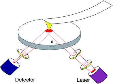 | ||
| Fig. 1 Scheme of the experimental setup. The optics is equipped with a detector- and a laser-arm operated at a fixed angle of incidence θ = (41 ± 1)°. The latter contains, besides the laser and a first λ/4 plate, a polarizer followed by a motorized compensator to obtain the desired state of polarization. The light reflected from the sample, which is coated onto a glass slide, passes through an analyzer and is detected by a photodiode. An additional lens, not shown here for clarity, is also located in the laser-arm, in order to focus the laser. The AFM tip, which is coated with a thin gold layer, is scanning the sample in contact mode (for details see text). | ||
Results and discussion
The Scanning Near-Field Ellipsometry Microscopy (SNEM) setup used here relies on a combination of a scanned, gold-coated AFM tip with an exact position control, provided by the closed loop AFM feedback circuit, and an optical illumination in specular reflection realized by the ellipsometer.5b In an experiment, the compensator and analyzer are initially moved until the null-ellipsometry conditions are found. This means that elliptically polarized light is sent to the sample at a fixed angle, such that the reflected light is linearly polarized. The latter is finally cancelled by the analyzer, hence in the absence of AFM tip–sample interactions no light reaches the photodiode detector.Subsequently, the gold-coated AFM tip is positioned over the same area illuminated by the laser spot using the AFM top-view camera. The sample is scanned in contact to record simultaneously a topographic image (from the AFM deflection feedback) and an optical image (from the optical detector output). The gold-coated AFM tip enhances the electromagnetic field in a highly confined area and near-field interactions cause some of the light to be scattered with altered state of polarization. The initially set null-ellipsometry condition is kept constant during the collection of the image, while the tip is scanned. Thus at each scanned point the interaction between the sample and the tip is monitored.
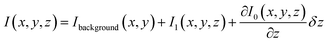
In general, three terms are expected to contribute to the overall optical signal, I: (i) a constant background at a fixed vertical position of the tip Ibackground, (ii) the near-field I1, and (iii) the contribution due to the vertical displacement of the tip as the system behaves like an inverted Fabry–Perot interferometer. In the approximation of small tip movement δz, the value of I(x,y,z) that corresponds to the situation described above can be written as:
 | (1) |
The first term is constant, thus it does not contribute to an intensity variation. The discrimination of the other two terms is crucial in order to visualize the optical near-field.
The dependence of the value of I(x,y,z) on δz was first determined by recording the optical signal, while performing a force–displacement measurement on glass. The deflection curve is not shown in Fig. 2 since these plots refer to the approach of the tip to the samples surface before contact, when no change of deflection was measured. Panel A shows the acquired data in gray. The oscillations of the signal in Fig. 2A are due to the interference between the light reflected from the cantilever/tip assembly and the light reflected from the sample, which has been minimized by setting the null-conditions. Hence a sinusoidal function was subtracted for all tip–sample distances from the thin gray line in Fig. 2A, to obtain the corrected optical signal as the thick black line. The slope for the data between the vertical dashed lines is a consequence of the approach of the metal coated cantilever, which is mounted under an angle with respect to the sample plane, into the area illuminated by the laser from below. This slope, as well as the background intensity observed for large tip–sample separation, was subtracted to obtain the corrected intensity plot shown in panel B.
 | ||
| Fig. 2 (A) Intensity vs. distance curve, obtained with a gold coated AFM tip simultaneously during acquisition of a force–displacement curve on glass (the force data are not shown in this figure). The point where the tip contacted the substrate could be unambiguously identified from the force–displacement data. (B) Intensity vs. distance curve corrected for the effect of background and interference (for details see text). | ||
The corrected intensity (Fig. 2B) decays steeply with increasing tip–sample distance. At a distance of ca. 50–75 nm it is already reduced to a factor of 1/e. This graph demonstrates that although the polarization of the incoming light is fixed by the sample (required to result in null-ellipsometry conditions to cancel the background light), a reasonable nanoscale localization of the tip–sample near-field interaction is obtained. Moreover, at distances above 100 nm, the signal approaches the noise level of the detector verifying a reasonable suppression of background scattering.
Near-field optical and AFM topographical data were subsequently captured on model samples supported on glass slides to analyze the lateral variation of the near-field optical signal during displacement in the (xy) plane. Fig. 3 and 4 show contact mode AFM images, as well as the photodetector output signal captured on a poly(methyl methacrylate) (PMMA) thin film30 that was loaded with 80 nm diameter silver nanoparticles. The Ag nanoparticles are clearly differentiated, i.e. both in the contact mode AFM height and the optical images, which display contrast due to the significant difference among the particles and the polymer in scattering of the incident light.31
 | ||
| Fig. 3 Silver nanoparticles in a PMMA film, as imaged with using a gold-coated tip (scan speed 280 nm s−1, the scale bar represents 100 nm): (A) AFM topography image (the z-scale covers 40 nm) and (B) optical image (the intensity covers 0–40 mV). | ||
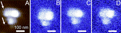 | ||
| Fig. 4 Silver nanoparticles in a PMMA film, as imaged with (A) contact mode AFM using a gold-coated tip (scan speed 3400 nm s−1, the z-scale covers 50 nm) and imaged using the optical setup at three different scan speeds: (B) 700 nm s−1, (C) 1750 nm s−1, and (D) 3400 nm s−1 (the z-scale covers 0–30 mV). | ||
The optical detector output provides an image with good contrast also for various scan rates between 700 and 3400 nm s−1, Fig. 4, compared to the AFM data, with a resolution below 80 nm. While the AFM images were found to be sensitive to the scan rate, the optical images showed only at the highest scan speeds some additional noise (compare Fig. 3D). Moreover, “jumping scan lines”, as observed for AFM (see arrows in Fig. 4A), were not observed in the corresponding optical images, Fig. 4D. In these lines the feedback controlled AFM tip moved up and down, but this movement in z-direction was not tracked by the optical image because the film was optically homogeneous.
The data displayed in Fig. 3 and 4 indicate a very close agreement between the two different imaging channels. This close match of topographical and optical images is attributed to the only partial embedding of the nanoparticles in the film, i.e. the particles protrude partially from the film resulting in a measurable topographic contrast. However, this close match is not necessarily the case. A detailed analysis of optical and force microscopy images acquired simultaneously on the Ag nanoparticle loaded PMMA films showed that the two imaging channels provide in many cases largely uncorrelated information (Fig. 5 and 6). While the image section displayed in Fig. 5 corresponds to a region of the PMMA film without any detectable nanoparticles but with a wavy topography, Fig. 6 shows data for completely embedded particles. For both scenarios the vertical tip movement does not correspond to changes in the optical signal, while a clear optical signal is detected in Fig. 6 in the absence of topographic contrast.
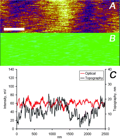 | ||
| Fig. 5 (A) AFM and (B) optical images captured simultaneously on the PMMA/silver nanoparticles sample, the scale bar represents 400 nm. (C) Height and intensity profiles of one scan line of the data shown in panels (A) and (B). | ||
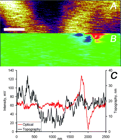 | ||
| Fig. 6 (A) AFM and (B) optical images captured simultaneously on the PMMA/silver nanoparticles sample, the scale bar represents 400 nm. (C) Height and intensity profiles of one scan line of the data shown in panels (A) and (B). | ||
A comparison of the force microscopy images (A) and the optical images (B), as well as the cross-sectional plots (C) provided for both situations, leads to the conclusion that the data are not well correlated. To analyze this quantitatively, the cross-correlation r for individual scan lines was calculated according to eqn (2):
 | (2) |
![[t with combining macron]](https://www.rsc.org/images/entities/i_char_0074_0304.gif) and ō are the average values for t and o.
and ō are the average values for t and o.
The value for the cross-correlation was found to be r = −0.28 for Fig. 4 and r = 0.13 for Fig. 6. These values indicate that the information obtained in the two imaging channels is not correlated in these cases and hence not redundant.
The second example studied, which exhibits significantly smaller dielectric contrast than the previous example,31 was a microphase-separated block copolymer film composed of polystyrene-block-poly(tert-butyl acrylate) (PS2092-b-PtBA1055). This polymer is known to microphase-separate with a cylindrical morphology and a typical repeat distance of ∼120 nm at the block length ratio used.32 This system served also as test sample for the setup proposed here, since high quality near-field images were recently reported by a parent technique, namely aperture-less near-field IR microscopy with homodyne detection and demodulation at the first harmonic.33Fig. 7B shows the optical image collected on a block copolymer film, while the AFM tip tracked the surface, with resolution compared to AFM data (Fig. 7A). The histogram of the pixels for the optical image (Fig. 7C) shows a bimodal distribution with ∼4 mV difference among the maxima corresponding to the PS and the PtBA phase, respectively. This contrast coincides with the different dielectric constants ε. The value of ε is higher for PtBA (εPtBA ≈ 3.5) compared to PS (εPS ≈ 2.5).34,35
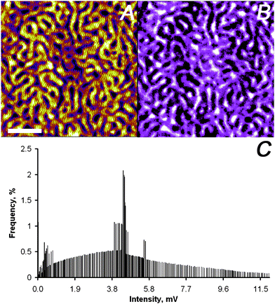 | ||
| Fig. 7 Simultaneously captured SNEM data of micro-phase separated PS2092-b-PtBA1055 block copolymer film on glass: (A) AFM height image (the scale bar represents 500 nm and the absolute roughness of the sample was 1 nm on a 3 μm × 3 μm scale), (B) optical image (the z-scale covers 0–12 mV), and (C) intensity distribution of optical image in panel (B). | ||
The optical image obtained in our SNEM approach cannot be considered to display pure dielectric contrast. The contributions of both dielectric contrast and topography, which are intrinsic to the near-field, must be taken into account. The presence of the latter contribution is often checked by comparing the topographical and the optical images, looking for a mismatch between the two figures.36 Indeed, for the block copolymer films a maximum correlation of simultaneously captured scan lines of r = 0.35 was found (for a relative shift of 2 pixels, corresponding to an offset of 20–30 nm), again indicating that the data are not well correlated (see also ESI†).
The contribution of the third term in eqn (1), i.e. , was further investigated by first scanning the sample in contact mode to collect the topographic profile by AFM. Afterwards the tip was scanned in a lift mode with a fixed vertical offset of 300 nm along the previously captured profile. This vertical off-set is beyond the reach of the rapidly decaying field of antenna effects and localized surface plasmons of the gold-coated AFM tip (compare Fig. 2). During this scan an “optical image” was recorded from the detector output, which can be considered to be free of near-field effects. Some residual contrast may be expected as the result of interference between the light reflected back to the detector at the glass slide holding the sample and the light reflected from the moving cantilever–tip assembly. However, the contrast observed in the optical image is extremely weak as shown in Fig. 8B and C, respectively. This result indicates that the optical data captured with the AFM tip in contact with the sample are dominated by the near-field contribution.
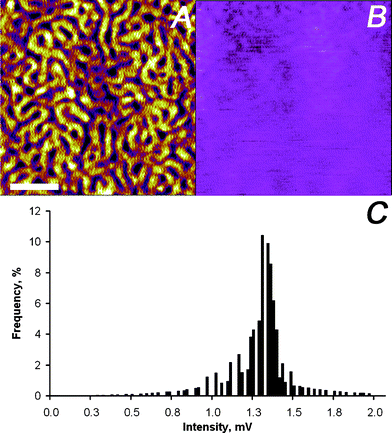 | ||
| Fig. 8 SNEM data of micro-phase separated PS2092-b-PtBA1055 block copolymer film on glass: (A) initially captured AFM height image (the scale bar represents 500 nm and the absolute roughness of the sample was 1 nm on a 3 μm × 3 μm scale), (B) optical image acquired with a vertical offset of 300 nm away from the previously captured sample surface profile (the z-scale covers 0–12 mV), and (C) intensity distribution of optical image in panel (B). For detail see text. | ||
To a first approximation, the gold coated AFM tip with its typical roughness can be considered as an ensemble of spheres with typical dimensions much smaller than the wavelength of the incident light, i.e., retardation effects can be neglected,37 or a rod-like structure.38 Electric field enhancement at a gold coated AFM tip is mainly due to both (i) the lightning rod effect, i.e. highly localized charge density,39–41and (ii) localized surface plasmon resonances.42–48 Recently Crozier et al.49 have demonstrated the existence of surface plasmons at gold coated AFM tips. However, plasmonic resonance is known to depend on the shape of the tip and thus the proper modeling of the interaction is difficult at present.50 Simulations that deal with near-field polarization effects have already been implemented.51 In the long run a thorough comparison of experiments and calculations will provide a more refined understanding of the physical interactions in the near-field zone.
The oscillating electric field arising from both effects mentioned above causes the electrons of the metal on the tip to oscillate coherently52 and a particle on the sample reacts to this field by becoming polarized, and then acts as a ‘mirror’ dipole, whose direction is parallel to the tip dipole. The mirror dipole interacts with the tip dipole, and thus the oscillating charge causes the conversion of the non-radiative tip mode into a propagating mode detectable in the far field.
Hence, in addition to the details of the setup, also the contrast mechanism differs fundamentally from the approach by Karageorgiev et al.29 Unlike in the setup of these authors, in which the sample was illuminated from below in total internal reflection (TIR) and the AFM tip scatters the near-field of the sample, in our SNEM approach the metal-coated AFM tip is illuminated through the transparent glass substrate from below. This leads to antenna effects and the excitation of localized surface plasmons at the gold-coated tip apex.
The exploitation of the localized, enhanced electric field at the tip apex in our experiments, rather than the evanescent field at the sample surface generated, e.g. by TIR,29 means that areas in parts of the sample other than the area close to the tip apex will not effectively perturb the images obtained. Therefore the imaging process is much more localized and does not require strong focusing of the laser spot. In general, LSPs are known to probe much smaller volumes than conventional surface plasmon polaritons. The electromagnetic field decay length is typically on the order of several nanometres for LSPs.52 Since the size and shape of the Au particle(s) at the end of apex are unknown, this distance was not well controlled. This would in principle be possible by attaching individual well characterized nanoparticles to AFM tips,53 hence the ultimate resolution can be much better than that shown in our experiments. By contrast, the decay length of the evanescent field created on the sample illuminated in TIR can be estimated to be on the order of 150 nm. The fundamental implication for our system is that an enhanced resolution can be expected, since the information is gathered in a small volume at the surface, where the confined near-field is strong. The data shown in this paper underline this assertion. Further investigations are in progress and highlighted already the possibility to extend the technique to imaging in intermittent contact mode AFM to avoid the sometimes considerable shear forces associated with contact mode AFM, which may damage soft matter or polymers.
Experimental
Materials
Poly(methyl methacrylate) (PMMA) with Mw = 15![[thin space (1/6-em)]](https://www.rsc.org/images/entities/char_2009.gif) 000 g mol−1 and silver nanoparticles (nominal diameter 80 nm) were purchased from Aldrich. A polystyrene-block-poly(tert-butyl acrylate), PS2092-b-PtBA1055 diblock copolymer (Mw 217500 and 135000, respectively for PS and PtBA blocks, polydispersity index (PDI) 1.10), where the subscripts denote the number of repeat units for each block, was purchased from Polymer Source Company (Dorval, Canada) and used as received.
000 g mol−1 and silver nanoparticles (nominal diameter 80 nm) were purchased from Aldrich. A polystyrene-block-poly(tert-butyl acrylate), PS2092-b-PtBA1055 diblock copolymer (Mw 217500 and 135000, respectively for PS and PtBA blocks, polydispersity index (PDI) 1.10), where the subscripts denote the number of repeat units for each block, was purchased from Polymer Source Company (Dorval, Canada) and used as received.
Sample preparation
A solution of PMMA and silver nanoparticles in toluene, with concentrations of 2 wt% and 0.2 wt% respectively, was spin coated on glass slides (Microscope Slides, 76 × 26 mm, Menzel GmbH Co. Braunschweig, Germany) at 500–2000 rpm for 30 s using a P6700 spin coater (Specialty Coating Systems Inc.). The glass slides were pre-cleaned with piranha solution (solution of 1:3 (v/v) 30% H2O2 and concentrated H2SO4) followed by rinsing with copious amounts of high-purity water (Millipore Milli-Q water). Caution: piranha solution should be handled with extreme caution; it has been reported to detonate unexpectedly.
PS-b-PtBA films were prepared by spin coating polymer solutions in toluene (15 mg mL−1) on glass slides, previously cleaned with piranha solution. The samples were spun at 3000 rpm for 30 s followed by drying in vacuum overnight.
SNEM
The setup comprised a MFP-3D AFM (Asylum Research, Santa Barbara, CA), a Multiskop ellipsometer (Optrel, Sinzing, Germany) and a custom-made interface plate (Optrel, Sinzing, Germany). AFM measurements were carried out in contact mode using gold-coated cantilevers equipped with integrated tips (type NPG, Veeco, Santa Barbara, CA) with a nominal spring constant of 0.12 N m−1 and a nominal thickness of the gold coating of 60 nm. Images were collected in air at scan rates in the range 400–3400 nm s−1 with 1024 × 1024 pixels2 resolution. Given the high number of pixels in one image, occasionally the images were median filtered to remove noise. The ellipsometer is equipped with a He–Ne laser emitting at a wavelength of 633 nm and was operated as described in the text with an angle of incidence of 41 ± 1°.54Conclusion
We described a Scanning Near-Field Ellipsometry Microscopy (SNEM) setup based on commercially available AFM and ellipsometry equipment, as well as gold-coated AFM tips, to obtain very high resolution optical images. The highly enhanced field caused by lightning rod effect and localized surface plasmons excited at the end of the gold-coated tip allowed us to image with an optical resolution below λ/10. Silver nanoparticles in a PMMA matrix, as well as micro-phases in block copolymers, were resolved based on the simultaneous acquisition of topographical and near-field optical data demonstrating the general applicability of the method to different classes of nanomaterials.Acknowledgements
The authors would like to thank Prof. Dr Motschmann and Dr Orendi (both Optrel GdbR) for insightful discussions and Joost Duvigneau for the preparation of the block copolymer thin film samples. Financial support by the Commission of the European Communities (Marie Curie RTN Contract Number MRTN-CT-2004-005516 BioPolySurf), NanoImpuls/NanoNed, the nanotechnology program of the Dutch Ministry of Economic Affairs and the MESA+ Institute for Nanotechnology of the University of Twente is gratefully acknowledged.Notes and references
- A. R. Clarke and C. N. Eberhardt, Microscopy Techniques for Materials Science, CRC Press, Boca Raton, 2002 Search PubMed.
- L. C. Sawyer, D. T. Grubb, and G. F. Meyers, Polymer Microscopy: Characterization and Evaluation of Materials, Springer, Berlin, 3rd edn, 2008 Search PubMed.
- P. J. Goodhew, J. Humphreys, and R. Beanland, Electron Microscopy and Analysis, Taylor & Francis, London, 2001 Search PubMed.
- R. J. Colton, A. Engel, J. E. Frommer, H. Gaub, A. Gewirth, R. Guckenberger, W. Heckl, B. Parkinson, and J. Rabe, Procedures in Scanning Probe Microscopies, Wiley, New York, 1998 Search PubMed.
- (a) A. Baba, W. Knoll and R. Advincula, Rev. Sci. Instrum., 2006, 77, 064101 CrossRef; (b) S. M. Flores and J. L. Toca-Herrera, Nanoscale, 2009, 1, 40–49 RSC.
- (a) T. Basche, W. E. Moerner, M. Orrit, and U. P. Wild, Single-Molecule Optical Detection, Imaging and Spectroscopy, VCH, Weinheim, 1997 Search PubMed; (b) W. E. Moerner and D. P. Fromm, Rev. Sci. Instrum., 2003, 74, 3597–3619 CrossRef CAS.
- G. Gouadec and P. Colomban, Prog. Cryst. Growth Charact. Mater., 2007, 53, 1–56 CrossRef CAS.
- S. W. Hell, Science, 2007, 316, 1153–1158 CrossRef CAS.
- A. Hartschuh, Angew. Chem., Int. Ed., 2008, 47, 8178–8191 CrossRef CAS.
- D. W. Pohl, W. Denk and M. Lanz, Appl. Phys. Lett., 1984, 44, 651–653 CrossRef.
- A. Lewis, M. Isaacson, A. Harootunian and A. Muray, Ultramicroscopy, 1984, 13, 227–231 CrossRef.
- Y. Inouye and S. Kawata, Opt. Lett., 1994, 19, 159–161 Search PubMed.
- C. H. Ullal, R. Schmidt, S. W. Hell and A. Egner, Nano Lett., 2009, 9, 2497–2500 CrossRef CAS.
- S. W. Hell and J. Wichmann, Opt. Lett., 1994, 19, 780–782 Search PubMed.
- E. Betzig, G. H. Patterson, R. Sougrat, O. W. Lindwasser, S. Olenych, J. S. Bonifacino, M. W. Davidson, J. Lippincott-Schwartz and H. F. Hess, Science, 2006, 313, 1642–1645 CAS.
- M. J. Rust, M. Bates and X. Zhuang, Nat. Methods, 2006, 3, 793–796 CrossRef CAS.
- T. Cordes, M. Strackharn, S. W. Stahl, W. Summerer, C. Steinhauer, C. Forthmann, E. M. Puchner, J. Vogelsang, H. E. Gaub and P. Tinnefeld, Nano Lett., 2010, 10, 645–651 CrossRef CAS.
- W. Grange, P. Haas, A. Wild, M. A. Lieb, M. Calame, M. Hegner and B. Hecht, J. Phys. Chem. B, 2008, 112, 7140–7144 CrossRef CAS.
- S. Aubert, A. Bruyant, S. Blaize, R. Bachelot, G. Lerondel, S. Hudlet and P. Royer, J. Opt. Soc. Am. B, 2003, 20, 2117–2124 Search PubMed.
- L. Gomez, R. Bachelot, A. Bouhelier, G. P. Wiederrecht, S. H. Chang, S. K. Gray, F. Hua, S. Jeon, J. A. Rogers, M. E. Castro, S. Blaize, I. Stefanon, G. Lerondel and P. Royer, J. Opt. Soc. Am. B, 2006, 23, 823–833 Search PubMed.
- T. Yano, T. Ichimura, A. Taguchi, N. Hayazawa, P. Verma, Y. Inouye and S. Kawata, Appl. Phys. Lett., 2007, 91, 121101 CrossRef.
- Z. Ma, J. M. Gerton, L. A. Wade and S. R. Quake, Phys. Rev. Lett., 2006, 97, 260801 CrossRef.
- J. N. Farahani, H.-J. Eisler, D. W. Pohl, M. Pavius, P. Flückiger, P. Gasser and B. Hecht, Nanotechnology, 2007, 18, 125506 CrossRef.
- H. G. Frey, F. Keilmann, A. Kriele and R. Guckenberger, Appl. Phys. Lett., 2002, 81, 5300.
- H. G. Frey, S. Witt, K. Felderer and R. Guckenberger, Phys. Rev. Lett., 2004, 93, 200801 CrossRef.
- T. H. Taminiau, R. J. Moerland, F. B. Segerink, L. Kuipers and N. F. van Hulst, Nano Lett., 2007, 7, 28–33 CrossRef CAS.
- B. Hecht, P. Mühlschlegel, J. N. Farahani, H.-J. Eisler, D. W. Pohl, O. J. F. Martin and P. Biagioni, Chimia, 2006, 60, 765–769 CrossRef CAS.
- P. Biagioni, J. S. Huang, L. Duo, M. Finazzi and B. Hecht, Phys. Rev. Lett., 2009, 102, 256801 CrossRef CAS.
- P. Karageorgiev, H. Orendi, B. Stiller and L. Brehmer, Appl. Phys. Lett., 2001, 79, 1730–1732 CrossRef CAS.
- S. Diziain, J.-M. Merolla, M. Spajer, G. Benvenuti, A. Dabirian, Y. Kuzminykh, P. Hoffmann and M.-P. Bernal, Rev. Sci. Instrum., 2009, 80, 093706 CrossRef.
- M. J. Weber, Handbook of Optical Materials, CRC Press, Boca Raton, 2003 Search PubMed.
- C. L. Feng, G. J. Vancso and H. Schönherr, Langmuir, 2005, 21, 2356–2363 CrossRef CAS.
- K. Mueller, X. J. Yang, M. Paulite, Z. Fakhraai, N. Gunari and G. C. Walker, Langmuir, 2008, 24, 6946–6951 CrossRef CAS.
- The phases in the AFM data can be assigned based on the assessment of the local mechanical properties by nanoindentation and modulus imaging using a Veeco Peakforce AFM. The elevated worm-like features in the AFM height image thus correspond to the stiffer PS phase.
- D. Fioretto, A. Livi, P. A. Rolla, G. Socino and L. Verdini, J. Phys.: Condens. Matter, 1994, 6, 5295–5302 CrossRef CAS.
- B. Hecht, H. Bielefeldt, Y. Inouye, D. W. Pohl and L. Novotny, J. Appl. Phys., 1997, 81, 2492–2498 CrossRef CAS.
- J. M. Pitarke, V. M. Silkin, E. V. Chulkov and P. M. Echenique, Rep. Prog. Phys., 2007, 70, 1–87 CrossRef CAS.
- S. Link, M. B. Mohamed and M. A. El-Sayed, J. Phys. Chem. B, 1999, 103, 3073 CrossRef CAS.
- L. Novotny, R. X. Bian and X. S. Xie, Phys. Rev. Lett., 1997, 79, 645 CrossRef CAS.
- R. Kappeler, D. Erni, C. Xudong and L. Novotny, J. Comput. Theor. Nanosci., 2007, 4, 686 CAS.
- C. C. Neascu, G. A. Steudle and M. B. Raschke, Appl. Phys. B: Lasers Opt., 2005, 80, 295 CrossRef CAS.
- M. Danckwerts and L. Novotny, Phys. Rev. Lett., 2007, 98, 026104 CrossRef.
- Y. C. Martin, H. F. Hamann and H. K. Wickramasinghe, J. Appl. Phys., 2001, 89, 5774 CrossRef CAS.
- J. T. I. Krug, E. J. Sanchez and X. S. Xie, J. Chem. Phys., 2002, 116, 10895 CrossRef.
- L. Novotny, Phys. Rev. Lett., 2007, 98, 266802 CrossRef.
- P. Mühlschlegel, H.-J. Eisler, B. Hecht and D. W. Pohl, Science, 2005, 308, 1607 CrossRef CAS.
- P. Olk, J. Renger, T. Härtling, M. T. Wenzel and L. M. Eng, Nano Lett., 2007, 7, 1736 CrossRef CAS.
- A. Alu and N. Engheta, Nat. Photonics, 2008, 2, 307 CrossRef CAS.
- Y. S. Zou, P. Steinvurzel, T. Yang and K. B. Crozier, Appl. Phys. Lett., 2009, 94, 171107 CrossRef.
- K. L. Kelly, E. Coronado, L. L. Zhao and G. C. Schatz, J. Phys. Chem. B, 2003, 107, 668 CrossRef CAS.
- (a) A. Madrazo and M. Nieto-Vesperinas, J. Opt. Soc. Am. A, 1997, 14, 618–628 CrossRef; (b) O. J. F. Martin, C. Girard and A. Dereux, J. Opt. Soc. Am. A, 1996, 13, 1801–1808 CrossRef CAS; (c) H. Furukawa and S. Kawata, Opt. Commun., 1996, 132, 170–178 CrossRef CAS; (d) H. Furukawa and S. Kawata, Opt. Commun., 1998, 148, 221–224 CrossRef CAS.
- K. A. Willets and R. P. Van Duyne, Annu. Rev. Phys. Chem., 2007, 58, 267–297 CrossRef CAS.
- Z. H. Kim and S. R. Leone, J. Phys. Chem. B, 2006, 110, 19804–19809 CrossRef CAS.
- A laser spot narrowly focused to the AFM tip would likely further increase the signal that reaches the detector. However, a relatively large laser spot of 200 μm in diameter, to be compared with the 80 μm maximum scan size for the AFM, was chosen in this work. This choice is justified in order to keep the instrument simple, as a smaller spot size would indeed imply the necessity to move all the optics according to the tip movement, for example when scanning large areas or when choosing different locations for the scanning process.
Footnotes |
| † Electronic supplementary information (ESI) available: A section of Fig. 7 and cross correlation. See DOI: 10.1039/c0nr00530d |
| ‡ Current address: University of Siegen, Department of Physical Chemistry I, Adolf-Reichwein-Str. 2, 57076 Siegen, Germany |
| § Current address: Scientific-Technical Services, Nanometric Techniques Unit, University of Barcelona, C/ Lluís Solé i Sabaris, 1–3, 08028, Barcelona, Spain |
| This journal is © The Royal Society of Chemistry 2011 |