2D materials: to graphene and beyond
Rubén
Mas-Ballesté
a,
Cristina
Gómez-Navarro
b,
Julio
Gómez-Herrero
*b and
Félix
Zamora
*a
aDepartamento de Química Inorgánica, Universidad Autónoma de Madrid, 28049, Madrid, Spain. E-mail: felix.zamora@uam.es; Fax: +34 91 4974833
bDepartamento de Física de la Materia Condensada, Universidad Autónoma de Madrid, 28049, Madrid, Spain. E-mail: julio.gomez@uam.es
First published on 16th September 2010
Abstract
This review is an attempt to illustrate the different alternatives in the field of 2D materials. Graphene seems to be just the tip of the iceberg and we show how the discovery of alternative 2D materials is starting to show the rest of this iceberg. The review comprises the current state-of-the-art of the vast literature in concepts and methods already known for isolation and characterization of graphene, and rationalizes the quite disperse literature in other 2D materials such as metal oxides, hydroxides and chalcogenides, and metal–organic frameworks.
 Rubén Mas-Ballesté | Rubén Mas-Ballesté was born in Barcelona (Catalonia, Spain) in October of 1975. In 2004 he got his PhD under the supervision of Prof. Pilar González-Duarte and Prof. Agustí Lledós. From June 2004 to November 2007, he worked in Lawrence Que's group at the University of Minnesota (USA) as a postdoctoral associate. At present, he is an associate professor under the “Ramón y Cajal” program at the Universidad Autónoma de Madrid (Spain). His research is focused on the reactivity of metal chalcogenides, synthesis and reactivity of structural and functional models of metalloproteins and inorganic materials for nanotechnology. |
 Cristina Gómez-Navarro | Cristina Gómez-Navarro, born in Madrid, Spain, obtained her PhD in physics at Universidad Autonoma de Madrid in 2005, focusing on electronic transport of carbon nanotubes and similar wired materials. Then she joined the group of Prof. Klaus Kern at the Max Planck Institute for Solid State Research (Stuttgart, Germany) as a Humboldt fellow, where she worked on chemically derived graphene. Since 2009, she has been working at the Universidad Autonoma de Madrid as a researcher. Her current interests are electronic and mechanical properties of 1D and 2D materials as well as development of scanning probe techniques. |
 Julio Gómez-Herrero | Julio Gómez-Herrero was born in 1963 in Madrid, Spain. He obtained his PhD at the Universidad Autónoma de Madrid and then he moved first to Berkeley, to work with Professor Miquel Salmeron and then to Purdue where he worked in Professor Reinfenberger's group. He is currently full Professor at the Universidad Autónoma de Madrid. His main research lines are scanning probe microscopy and electrical transport at the nanoscale. |
 Félix Zamora | Félix Zamora was born in 1967 in Cuenca (Spain). In 1994 he obtained his PhD in Inorganic Chemistry at Universidad Autónoma de Madrid. He moved to the University of Dortmund (Germany) to work with Professor B. Lippert. He is currently “Profesor Titular” at the Inorganic Chemistry Department at the Universidad Autónoma de Madrid. From 2004 he focused on new nanomaterials based on inorganic systems such as coordination polymers. |
1. Introduction
Nanomaterials is the field of material science devoted to the study of materials with at least one dimension in the nanometre scale.1 At this scale, qualitative changes in physicochemical properties and reactivity are connected to the number of atoms or molecules forming the material. For instance, size-effect properties can be observed, such as surface plasmon resonance in metal nanoparticles, quantum confinement in semiconductor particles and superparamagnetism in magnetic nanomaterials.If only one dimension is restricted, we will have a layered shape or 2D material; if two dimensions are limited in size, we will have a wired or 1D material; if all dimensions are in the range of a few nanometres we usually talk of 0D materials.
Therefore, it is not only size but also dimensionality that is one of the most defining parameters when determining material properties. This particularly applies to the case of sp2carbon materials (Fig. 1), where 0D fullerenes, 1D nanotubes, 2D graphene and 3D graphite exhibit very different properties. Also, when it comes to analyzing the chronological order of the findings of the different dimensional forms of a given material, the case of carbon is a representative example: Graphite has been known since the sixteenth century and has been widely used in industry for steel-making, as brake lining or as dry lubricant in some other devices. But it was not until 1985 when the discovery of fullerenes2 greatly expanded the number of known carbon allotropes and furthermore suggested the existence of its 1D form, carbon nanotubes, which were first demonstrated in 1991.3 Although the theoretical studies of graphite, fullerenes and nanotubes were performed using a single layer of graphite as starting material, it was not until 20044 that scientists were able to isolate a monolayer graphene sheet for the first time. The recent blossoming of graphene literature evidences not only its basic scientific interest but also its potential technological impact. Actually, two dimensional materials are expected to have a significant impact on a large variety of applications, ranging from electronics to gas storage or separation, catalysis, high performance sensors, support membranes and inert coatings, just to mention a few of them.
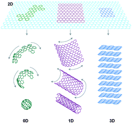 | ||
| Fig. 1 Graphene can be envisaged as a 2D material for carbon materials among all other dimensionalities. It can be wrapped up into 0D buckyballs, rolled into 1D nanotubes or stacked into 3D graphite (Taken from ref. 6. Reproduced by permission of Nature Publishing Group). | ||
A large number of articles and reviews have been published on synthesis and physical properties of graphene. Prompted by these findings a variety of novel 2D materials have recently started to appear but the literature that one can find on this topic is still moderate and quite disperse. In order to have a unified vision of the field, this review attempts first, to summarize how the vast literature in concepts and methods already known for isolation and characterization of graphene, can be applied to a whole new family of 2D materials. Secondly, new perspectives and potential applications of these 2D materials are provided.
2. Graphene: the first example of a big family
Graphene, a single layer of graphite, has been one of the first real two dimensional materials (i.e. one atom thick) to be isolated in nature. During the last five decades, an extensive effort was invested in obtaining single layers of graphite (graphene sheets), with the aim of having access to the predicted properties of a tightly bond one-atom thick layer of sp2carbon. In fact, many techniques had been tested in the past with only moderate success. Most of the reported works until the mid 1990s were focused on graphite intercalation compounds. In these compounds, a host molecule or atom gets “sandwiched” between the graphite layers, resulting in a weakening of interplanar forces and facilitating separation of layers. Among these compounds the use of expandable graphite, a compound that can expand in volume by a factor of up to 1000 upon rapid heating, was widespread during the 1960s, but the best results were materials with few (10–50) layers.Many other more sophisticated techniques were tested and reported during the next decades with only moderate success, since the thinner flakes observed were around 10 layers.
Eventually, single layers of graphite were first isolated by Andre Geim's group, at Manchester University in 2004.5 The reported technique for obtaining real one atom thick layers with almost macroscopic lateral dimensions is really simple. It consists of rubbing HOPG (highly oriented pyrolitic graphite) against another surface (like using a pencil). This leaves a variety of flakes on the surface. Most of these flaky materials are composed of more than ten layers, but surprisingly, among the resulting structures single layers can also be found. As important as the technique is the reported method for detection of single layers in this work. One atom thick layers of almost any material are transparent to visible light. However, they become slightly visible on top of an oxidized silicon substrate, where the change in optical path due to the monolayer is enough to change the interference colour with respect to the bare substrates (this is usually known as phase contrast). Despite the simplicity of the cleaving method, the very low yield of monolayers does not make it a reliable and cost-effective technique for coating large silicon wafers, thus not technologically applicable. However, it is useful for fundamental studies, as demonstrated by the large amount of works carried out using this technique (see ref. 6 and references therein), and more importantly, it proves that real high crystal quality two dimensional materials are stable under ambient conditions and are continuous on a macroscopic scale. Therefore, this result has triggered a tremendous effort in the materials science community in the search of other ways to produce graphene sheets.
In this respect, reasonable success has been achieved by hydrocarbon decomposition at high temperature (CVD) that leads to catalytic assisted growth of graphene on certain metal crystals7,8 such as Ir, Ru and Pt. In addition, graphitization of SiC in an ultrahigh vacuum at high temperatures leads to graphene layers on the insulating SiC substrate.9 However, these two techniques are substrate-limited and require both high vacuum and/or temperature which makes them really costly. A series of bottom-up or self-assembly approaches have also been used to synthesize graphene structures. These methods use organic precursors with at least three functional groups as building blocks, in other words, three potential sites capable of covalent bond formation with other molecular connectors. So far, these synthetic procedures give graphene with reduced dimensions (smaller than 100 nm2), the so-called nanographenes.10
So, given the limits of the mentioned approaches, a huge effort is being invested in solution based techniques, which are expected to be easily scalable and economical, affording mass production of graphene.
Some success has been achieved in obtaining suspensions of organic-molecule-coated graphene sheets using expandable graphite,11 but removal of the coating always leads to re-aggregation of graphene sheets into graphite. After an intensive and extensive search for appropriate solvents, colloidal suspensions of graphene sheets have been obtained by sonication of graphite in organic solvents such as NMP12 (N-methylpyrrolidone). Unfortunately, the concentration of the suspension and yield of single layers were quite low and work in improving these two issues is still needed.
A promising solution approach to overcome the low solubilization of graphite in any solvent seems to be the use of graphite oxide as starting material.13 Although the exact chemical structure of graphite oxide is still debated,14,15 we do know that graphite oxide consists of a layered material composed of “graphene oxide” sheets where the carbon network is strongly disrupted and a significant fraction of the carbon atoms bears hydroxyl groups or participate in epoxide groups. The presence of these functional groups reduces the interplanar forces and imparts hydrophilic character to the material, making possible complete exfoliation of single graphene oxide (GO) layers in aqueous media with only the aid of stirring or mild sonication. Thus, high concentration and yield of single layers can be obtained in solution by this simple process. In contrast to graphene, GO is a good insulator, due to the disruption of the aromaticity of graphite. As good electrical conductivity is desirable for many of the potential applications of graphene, substantial efforts have been directed to recovering its original conductivity. Deoxygenation has been shown as a workaround for this problem. Removal of oxygen atoms substantially enhances GO electrical conductivity by partially restoring the aromatic carbon network. In this respect, significant advances have been made in the last years through the improvement of reduction methods for better conductivity16,17 that now approaches the one observed in micro-exfoliated graphene sheets. In fact, thin films of chemically reduced graphene oxide are currently considered to be good candidates to substitute metal oxides as electrodes in solar cells18,19 since they are highly transparent and fairly good electrical conductors.
3. 2D materials beyond graphene
In view of the success obtained in the search for graphene layers, the ideas and methodology learnt in these studies have been extended to other layered materials. Thus, graphene is becoming a cutting edge material that opens up new horizons to a whole new variety of possibilities beyond the limited current applicability of graphene. Fortunately, it is not only graphite that responds to the idea of pulling out one layer from a three dimensional material with strong covalent in-plane bonds and weak van der Waals-like coupling between layers. Examples of 2D inorganic nanomaterials blossomed during the last years. Consequently, specific reviews on exfoliation of determined families of layered materials and their reassembly into new stacked products have appeared in the last few years.20–22 In the present work we offer a brief overview of the successes reported on the isolation and characterization of 2D materials. But, before going any further, in order to clarify concepts, an operational definition of a 2D material is required: in this review we understand 2D materials as those that do not require a substrate to exist. In other words, they can be isolated as freestanding one atom thick sheets. This definition can be relaxed to include materials with a thickness of a few atoms (less than 10). This review is not intended to be an exhaustive compilation of all the literature on this field. We just present a collection of representative recent examples that illustrate the different materials and methodologies that are relevant on the quest of 2D materials. As a criterion, we selected the references that include AFM evidences of the morphology of the materials because this technique is the most reliable to determine the thickness of a layer deposited on a surface in order to assess that what is obtained is really a 2D material.In this section we summarized the reported alternative 2D materials. The description has been ordered according to their preparation methods. It is noteworthy to stress that epitaxial growth has not been considered since materials growth by this method are surface dependent.
3.1 Micromechanical exfoliation
In addition to graphite, micromechanical exfoliation methodology has been extended to other inorganic materials. In fact, following this approach, individual crystal sheets from a variety of layered materials have been isolated. Monolayers of BN, MoS2, NbSe2 and Bi2Sr2CaCu2Ox have been prepared by rubbing a fresh surface of a layered crystal against another surface, leaving a variety of flakes attached to it.5 Among the resulting flakes, single layers were always found. The resulting 2D materials so obtained exhibit high crystal quality and macroscopic continuity, as in the case of graphene. A facile screening of the resulting flakes can be done by optical microscopy. Further correlation between optical images and AFM measurements can result in a fast estimation of the thickness distribution of the flakes obtained by the “rubbing method”. This is a critical point because single layers are in a very minor proportion in comparison with thicker structures and, consequently, in practice, it would be impossible to find cleaved 2D crystallites by scanning surfaces at random by AFM. However, their tentative identification in an optical microscope when they are placed on top of an oxidized Si wafer made it possible to guide the search for 2D crystallites by AFM. Further scanning tunneling, scanning electron, and high resolution transmission electron microscopy (HRTEM) studies on monolayers of BN, MoS2, NbSe2 and Bi2Sr2CaCu2Ox confirmed that the prepared 2D crystallites remained monocrystalline under ambient conditions and no degradation was noticed over periods of many weeks. Within experimental resolution, the crystal structure of isolated layers remained the same as for stacked layers within 3D crystals.Therefore, micromechanical exfoliation, as originally used with graphite, is the easiest and the fastest method to obtain 2D materials. In fact, according to the reported experimental procedure, the whole process to generate and identify probable 2D crystallites takes literally half an hour. However, as explained for graphene, this is a method that has important drawbacks: monolayers obtained by micromechanical exfoliation are in a great minority among accompanying thicker flakes, making this technique not scalable for larger production. Consequently, despite allowing the first examples of characterization of one-atom-thick monolayers, this is not a feasible procedure for large scale production of 2D materials for technological applications. Thus, analogously to what has been accomplished for graphene, in the last few years, new methods have been developed to obtain 2D inorganic materials.
3.2 Surface assisted in situgrowth
In close analogy to the growth of graphene by thermal decomposition of hydrocarbons, generation of one-atom-thick films has been achieved by in situ chemical reactions on a surface. The role of the surface in this approach is different to that in an epitaxial growth. In the growth assisted method the surface does not serve as a seed crystal but rather as a catalyst or merely a template. Initially, this methodology did not allow the unraveling of the important question of whether 2D materials would exist independently of a surface. The main advantage of this methodology is that clean single layers without accompanying thicker flakes can be isolated.This template method has allowed isolation of BN hollow nanoribbons.23 The template used was ZnS nanoribbons, chosen according to the following criteria (Fig. 2): a) ZnS nanoribbons can be easily synthesized in a large quantity by CVD; b) under H2, ZnS vaporizes at 1100 °C while BN does not vaporize until 3000 °C, so that replicated BN can be preserved when the ZnS template is removed by vaporization; c) both ZnS and BN have a hexagonal structure which avoids mismatching that could cause corrugation. The novel BN nanostructures obtained by this method have distinct structural and optoelectronic characteristics when compared with other forms of BN nanostructures, as shown by Raman, infrared, UV-vis, and cathodoluminescence spectroscopies.
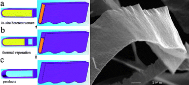 | ||
| Fig. 2 Schematic representation of the steeps following in the surface assisted in situgrowth. (a) Cross section and section of ZnS/BN belt heterostructure. (b) Intermediate heterostructure following partial vaporization. (c) Hollow BN nanostructure. Low magnification SEM image of a BN nanoribbon showing its general morphological features (Taken from ref. 23. Reproduced by permission of the American Chemical Society). | ||
As shown in the preceding example, the surface assisted growth of monolayers allows control of the patterning and the structure of such materials that can be yielded free of thicker by-products. However, this strategy is very dependent on the interaction between the template surface and the nanosheet, and thus, it is not widely applicable. Also, often high temperatures are required. To overcome these problems new approaches have been made recently on extensive exfoliation of layered materials.
3.3 Exfoliation into colloidal solutions
The main limitation of the micromechanical exfoliation method is the large thickness of the majority of the resulting crystals. As an alternative, obtention of colloidal solutions allows easy discrimination by size (i.e. by means of centrifugation), making isolation of single layers separately from thicker structures possible. These procedures have attracted much attention as an efficient method for preparing single layers with lateral sizes of up to several micrometres. Pioneering works in this line appeared in the 1990s, reporting the obtention of colloidal suspensions, which showed spectroscopic features suggesting that exfoliation allowed the obtaining of single layers.24–27 Indeed, it was during the following decade that AFM measurements confirmed that single layers were isolated. Below, we report the studies that present AFM evidences of exfoliation into single layers (Table 1). Methods to achieve this goal deal with the factors that allow the disruption of the interlayer interactions. Prompted by the findings related to graphene isolation, several strategies can be found in the literature. Inspiration can be found in the oxidation of graphite to obtain graphene oxide containing functionalities that result in repulsive forces and thus exfoliation. Thus, methods based on a chemical modification of the layers that result in repulsive forces between layers allowed formation of colloidal solutions.| Single layer composition | Obtention method | Intercalator | Reference |
|---|---|---|---|
| MnO2 | a) Protonation | TBA+ | 28 |
| b) H+–BA+ exchange | |||
| TBAxH(1.07−x)Ti1.73O4·H2O | a) Protonation | TBA+ | 32 |
| b) H+–TBA+ exchange | |||
| CoO2− | a) Protonation | TMA+ | 29 |
| b) H+–TMA+ exchange | |||
| TBAxH(1−x)Ca2Nb3O10 | a) Protonation of KCa2Nb3O9 | TBA+ | 33 |
| b) H+–TBA+ exchange | |||
| Bi2SrTa2O9 | c) Protonation | Ethylaminomium | 37 |
| a) H+–Ethylammonium exchange | |||
| Cs4W11O362− | a) Protonation | TBA+ | 38 |
| b) H+–TBA+ exchange | |||
| Ni(OH)5/3DS1/3 | a) Direct synthesis of Ni(OH)2−xDSx | DS− | 39 |
| b) Reflux in formamide | |||
| Eu(OH)2.5(DS)0.5 | a) Cl−–DS− exchange in Eu(OH)2.5Cl0.5 | DS− | 40 |
| b) Stirring in formamide | |||
| Co2/3Fe1/3(OH)21/3+ | a) Oxidation of Co2/3–Fe1/3(OH)2 LDH to Co(II)–Fe(III) with I2 | ClO4− | 41 |
| b) Exchange of interlaminar I− by ClO4− | |||
| c) Sonication in formamide | |||
| [Cu2Br(IN)2]n | Sonication in aqueous solution | — | 49 |
In the case of metal oxides, protonation usually resulted in electrostatic repulsions that facilitated exfoliation. By this procedure single layers of manganese28 (Fig. 3), cobalt,29 tantalum,30ruthenium31 and titanium32oxides as well as sheets of several perovskite type structures—H2[An−1BnO3n+1] (A = Na, Ca, Sr, La; B = Ta, Ti33), K2Ln2Ti3O10, KLnNb2O7, and RbLnTa2O7 (Ln = lanthanide ion),34HMWO6 (M = Nb, Ta),35KCa2Nb3O10,36KSr2Nb3O10,36Bi2SrTa2O937 and Cs4W11O362–38—have been separated from bulk samples. In these cases a chemical intercalator that assists the separation of layers and hampers the reassembly of the bulk laminar material is always required. Tetrabutylammonium (TBA) is the most commonly used intercalator, but also tetrametylammonium (TMA) and ethylammonium have been used successfully for these proposes. This concept is closely related to the intercalation phenomena described for graphite where bulky organic molecules expanded the laminar structure of graphite decreasing interlaminar interactions.
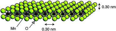 | ||
| Fig. 3 Model of a single layer of MnO2 (Taken from ref. 28. Reproduced by permission of the American Chemical Society). | ||
Generally, AFM measurements of samples of colloidal solution of metal oxides adsorbed onto a surface revealed flat two dimensional structures. The thickness of such structures was measured at steps between the layers and the substrate surface showing values between 0.9 and 2 nm depending on the crystallographic thickness of layers in the laminar bulk starting materials (Fig. 4). Lateral dimensions generally observed are commonly in the range of several hundred nanometres. However, the lateral dimensions are highly dependent on the crystallinity of the bulk starting materials. Accordingly, exfoliation by proton exchange of large single crystals (with lateral size of over 1 mm) of a potassium lithium titanate, K0.8Ti1.73Li0.27O4 resulted in very large nanosheet crystallites of H1.07Ti1.73O4·H2O with a lateral size of several tens of micrometres.32 It is commonly observed that the AFM measured height is slightly thicker than the crystallographic thickness of individual layers. This general observation is attributed to the presence of hydration layers or intercalator ions resulting in a surface-sheet interface of a thickness between 0.5 and 1 nm.
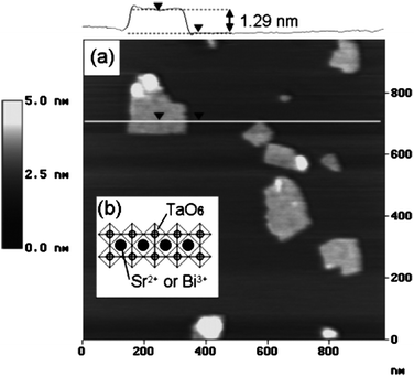 | ||
| Fig. 4 Structural model of a Bi2SrTa2O9 layer and its AFM topography image (Taken from ref. 37. Reproduced by permission of the American Chemical Society). | ||
Another strategy used for the exfoliation of layered metal hydroxides is the insertion of a bulky intercalated agent such as dodecyl sulfate (DS) ions. Nice control of the shape of the isolated layers is achieved by this technique, and formation of hexagons of nickel hydroxide was reported following this procedure.39 In this case, exfoliation was induced by intercalation of DS ions into the Ni(OH)2 under reflux in formamide. AFM images show lateral dimensions of several hundreds of nanometres and homogeneous thickness of 1.1 nm, again larger than that estimated from crystallographic data because of absorption of water and DS ions (Fig. 5).
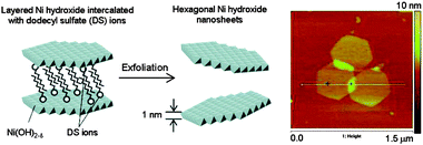 | ||
| Fig. 5 Schematic representation of the dodecyl sulfate ion intercalation between the nickel hydroxide layers and AFM topography image of the isolated hexagonal layers (Adapted from ref. 39. Reproduced by permission of the American Chemical Society). | ||
Analogously, exfoliation of layered europium hydroxide intercalated with dodecyl sulfate was carried out in formamide, producing unilamellar sheets.40 First, the DS-intercalated layered europium hydroxide was obtained by an anion-exchange from the Eu(OH)2.5Cl0.5·0.9H2O precursor. DS anion exchange causes the enlargement of basal spacing from 0.87 to 2.46 nm as indicated by X-ray diffraction, which facilitates further exfoliation. AFM analysis of the exfoliated product revealed sheet-like objects with a lateral size of several hundred nanometres. The height profile revealed that the sheets had a flat surface with a thickness of 1.6 nm, corresponding to a single layer of the layered europium hydroxide. The deviation between the AFM thickness and the crystallographic interlayer distance (0.7 nm) is, once more, attributed to the adsorption of DS anions as well as molecules of solvent.
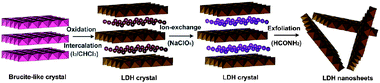
An alternative method for obtaining single/few layers is based on the observation that extensional forces induced by ultrasound can break weak interlayer interactions. An innovative approach based on a combination of, firstly, chemical modification of a layered hydroxide compound and later ultrasonic exfoliation was reported for the transformation of brucite-like Co2+–Fe2+ hydroxides into hydrotalcite-like Co2+–Fe3+ layered double hydroxide (LDH).41 In the brucite-like bimetallic hydroxides, divalent cobalt and ferrous cations are homogeneously located in octahedral hydroxyl sheets. Reaction of the brucite-like crystals with iodine results in the formation of an LDH phase in which anions (I−) occupy the interlayer space to balance the extra positive charges carried by the oxidization of Fe2+ into Fe3+. Exchange of iodide anions by perchlorates allowed further exfoliation into unilamellar sheets by an ultrasonic treatment in formamide (Fig. 6). Morphology and size of the exfoliated sheets were examined by AFM showing lateral dimensions of several hundreds of nanometres on the Si wafer. The ultrathin sheets are somewhat irregular in shape, indicating possible severe breakage or fracture during ultrasonic delamination. The height profile of the sheets reveals an average thickness of 0.8 nm, demonstrating the unilamellar nature of the sheets.
 | ||
| Fig. 6 Schematic representation of the synthesis and exfoliation of hydrotalcite-like Co2+–Fe3+ layered double hydroxide (Taken from ref. 41. Reproduced by permission of the American Chemical Society). | ||
Despite the reported success in isolating single layers of metal oxides and hydroxides, in the search for applications these kinds of materials offer scarce opportunities for design. Indeed, variations on structure and properties can only be envisaged as a consequence of changing metal centres. Alternative materials with a wide range of physical and chemical properties, as well as tunable architectures, are those named coordination polymers, also known as metal–organic frameworks (MOFs). Since they are formed by the assembly of different building blocks, their suitable selection allows a rich variety of architectures and dimensionalities.42 In fact there are numerous examples of layered structures derived from coordination polymers obtained in the crystal phase as lamellar materials. However, nanomaterials based on these systems are still scarcely explored.43 Regarding 2D coordination networks, there are few reports on ordered monolayers generated by vapour-deposition techniques on metal substrates under ultrahigh vacuum conditions. Scanning tunnelling microscopy images show an impressive level of order in these systems.44,45 However, these techniques require complex instrumentation and the areas of crystalline 2D materials are often limited to several nm2 which are appropriate for STM studies but inconvenient for most of the technological applications.
The bond strength of coordinative bonds is considered to be smaller than covalent C–C bonds and aspects concerning not only thermodynamic stability but also kinetics of the metal–ligand bonds could, in principle, suggest instability of these materials towards single-layer isolation. These aspects have recently been discussed in an excellent review on 2D polymers.10 However, the features of the coordinative bonds highly depend on the specific metal ion and the ligand. Therefore, aspects concerning reversibility of metal–ligand bonds (which occurs under specific energetic conditions46–48) are largely influenced by the specific nature of both building blocks (metal ion and ligand). Thus, a recent report presents exfoliation of single layers extracted from crystals of [Cu2Br(IN)2]n (IN = isonicotinato) generating a colloidal suspension.49 The planar nature of the layers observed in the crystal structure and the multifunctional properties found for this coordination polymer made it an attractive candidate to generate a 2D crystallite. To reach this goal, sonication was chosen as the mechanical force to remove the interlayer interactions analogously to several methods used to isolate graphene from graphite. Thus, casting deposition of diluted sonicated solutions of the compound on highly oriented pyrolytic graphite (HOPG) allows isolation of monolayers (Fig. 7). AFM analysis showed a very dense and homogenous distribution of flakes with typical observed heights of 0.6 nm, in good agreement with the X-ray data. XPS analysis of the isolated layers is in agreement with the composition of the starting material.
![(a) Schematic representation of a single layer of [Cu2Br(IN)2]n (IN= isonicotinato). (b) AFM topography image of [Cu2Br(IN)2]n deposited on HOPG. (c) Height profile across the green line in (b) (Taken from ref. 49. Reproduced by permission of the Royal Society of Chemistry).](/image/article/2011/NR/c0nr00323a/c0nr00323a-f7.gif) | ||
| Fig. 7 (a) Schematic representation of a single layer of [Cu2Br(IN)2]n (IN= isonicotinato). (b) AFM topography image of [Cu2Br(IN)2]n deposited on HOPG. (c) Height profile across the green line in (b) (Taken from ref. 49. Reproduced by permission of the Royal Society of Chemistry). | ||
In addition to the methods presented above, direct synthesis seems to be a straightforward alternative. Interestingly, in a recent report reaction from two simple precursors, Fe(CO)5 and the elemental chalcogens (Se and Te), in the presence of surfactant has allowed isolation of single layers of PbO-type β-FeSe, and composition-tunable Fe(Se,Te).50 This example represents the unique work on direct synthesis procedure. The well-known bulk properties of the metal chalcogenide materials, such as superconductivity, suggest a wide range of future technological applications.
4. Properties: What is so special about 2D materials?
What makes 2D materials attractive? Are their properties different from its respective 3D structure? As we mention in the introduction, restrictions of size in one or more dimensions effectively changes some properties of materials. So, in general, we expect 2D materials to differ in some properties from their bulk form. Optical and electronic properties are usually different due to confinement of electrons but also due to the absence of interlayer interactions, that, despite being generally quite weak, play an important role in determining band structure. Some other changes in properties, such as mechanical and chemical response, are mainly due to geometry effects and to the high (even infinite in the thinnest materials) surface-bulk ratio.4.1 Graphene: the reference sample
Although graphene offers a whole new range of unusual properties to investigate, to date most of the research has been focused on its electronic properties. Many (but not all) of the extraordinary features of graphene derive from the combination of its dimensionality and its very peculiar electronic band structure where the electrons mimic relativistic particles.6 This is why electrons in graphene are usually called massless Dirac Fermions51 and can be seen as electrons that have lost its rest mass (of course, the electrons as fundamental particles preserve their characteristic mass). This curious behaviour of the electrons makes graphene ideally suitable to study relativistic effects in condensed matter experiments. To date, the most remarkable consequences of this behaviour are the appearance of an atypical quantum Hall effect,51,52 first observations of Klein paradox53,54 and the study of relativistic phenomena as the Zitterbewegung, or jittery motion of the wave function in the presence of confining potentials. This peculiar band structure is modified to a more common one when more than three layers of graphene are stacked.In addition, the valence and conduction band in graphene touch each other at a single point55 (Fig. 8), offering very few electronic states near the Fermi level. For this reason graphene is usually called a semimetal or a zero gap semiconductor. The fragility of a single point contact makes the band structure of graphene highly sensitive to any change, such as external electric fields, mechanical deformations, doping and adsorbates, which is very desirable for sensing applications. This also confers an ambipolar character onto graphene, i.e. charge carrier can be either holes or electrons depending on doping.4 However, chemical doping is not always needed to change the charge carrier sign (it can be changed by local electric fields). This property opens the door to electrical engineering by creating p–n junctions with high mobilities, the base of current CMOS technology.
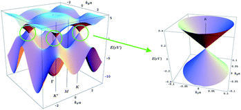 | ||
| Fig. 8 Three dimensional representation of the electronic band structure of graphene. The region near the Fermi level in one K point has been enlarged in the right panel. Two cones touching at a single point can be clearly seen here. | ||
Microscopic studies prove that graphene also exhibits outstanding crystal quality in scales as large as a few microns.56 The absence of defects or imperfections makes electrons free to travel distances as long as a few micrometres without scattering, even in samples placed on rough substrates. The lack of scattering results in huge mobilities57 of the charge carriers and give access to the observation of quantum phenomena, such as the quantum Hall effect, even at room temperature.58 In addition, the high number of moieties observed in graphene (about 1000 higher than in silicon) are an important for achieving electronic circuits with much faster switching rates.
Some properties of graphene that derive strictly form its two dimensional nature are also very attractive. Its extreme thickness (smaller than the electric screening length of 5 Å) gives access to observation of field effects in the conductance of the samples, which is highly desirable for applications in electronics and sensing. In a three dimensional graphite structure, the effect of an electric field in a mono- or bi-layer is hidden by the behaviour of the rest of the layers, where the external electric field will be completely screened. In addition, all electron waves are accessible to scanning probes and other surface techniques which, in this case, will allow full characterization of the material since it is only one atom thick. Its low dimensionality also makes graphene prone to take part in proximity effects such as superconductivity59 or ferromagnetism.
Very related to the electronic band structure of graphene are its optical properties. The absence of a band gap makes the absorption of light in a large range of the electromagnetic spectrum possible, spanning from the infrared to the ultraviolet,60 and giving rise to a vast number of possibilities of electronic transition which open a huge potential both for applications in electronic-photonic devices and fundamental studies.61 At the same time, due to their thickness, and despite being quite opaque for a single atomic layer, thin films of graphene present absorbance of less than 10% (2.3% for a single layer).62 This high transparency combined with their good conductivity makes them ideal candidates to substitute current metal oxides as transparent electrodes in devices such as solar cells or liquid crystal devices.18,19 Although this is certainly a very attractive topic, the optical properties of graphene are probably one of the most unexplored aspects of this new material, but definitively the optical properties by itself and the interplay between electrical and optical properties will bring new fields into graphene research.
Similar to diamond, and due to the high strength of the carbon–carbon bond, graphene is one of the strongest materials ever tested. It presents an extremely high breaking strength,63 200 times higher than steel, but at the same, it is also unexpectedly flexible. It can sustain elastic deformations of more than 20% and, due to its 2D nature, it also presents unprecedented high pliability. Pleats and folds are quite often found without the need for rupture.56 However, it is also said to be a brittle material, since it breaks like glass at very large strains. In summary, the strength of the bonds combined with its 2D nature also makes graphene an exciting material from a mechanical point of view.
Last but not least, the chemistry of graphene is also of major interest and it is currently the centre of attention of state of the art experiments. One might tend to think that the chemistry of graphene is the same as graphite. The experimental facts have now shown that although the chemistry of graphite can be used as guidance, there are some important differences. The corrugation characteristic of graphene seem to produce very local (nm scale) reactivity, different from graphite. In addition, the fact that chemical species can attach to both sides of graphene allows some chemical bonds that would be unstable in the case of graphite.64 And third, changes induced chemically in the properties of graphene are much more pronounced than in the case of graphite, since there is no contribution from the bulk. In this respect it has been shown that functionalization of graphene both with hydrogen or oxygen can induce a metal to insulator transition;65,66 chemical doping can be produced with different metals and ions.67 Mechanical properties might also be tuned by the presence of functional groups or defects.68 All this chemistry is also suitable to be produced locally, allowing the production of all graphene devices with different regions of different properties.69,70
4.2 The properties of other 2D materials
A huge effort has been made in a record time in the research of graphene properties. It is important to remark that almost all the experimental studies performed on graphene have been done in the solid state on isolated layers deposited on different substrates. Contrary to the case of graphene, for the already reported variety of other single layered materials, investigations of their physicochemical properties are still limited and most of them have been performed on colloidal suspensions and focused on their optical (absorption-emission) properties. It is also true that reassembly of exfoliated layers resulted in formation of new layered materials with properties that open applications such as supercapacitors,71,72 photo-conducting cells,73,74 p–n junctions,75 or as low-dimensional magneto-opical nanostructures.76–78 In addition, organic-inorganic layered materials is a field of high current interest due to the potential towards materials with multifunctional properties.79 Despite the obtention of these layered materials is of high interest, as stated in the introduction section, those are not the subject of this review. Thus, we started by summarizing the peculiar case of graphene and at this point we will review the studies found in the literature for other 2D structure properties.Due to the intrinsic properties of the inorganic materials isolated as single layers, the optical properties of some of them have been reported showing remarkable aspects. Thus, the BN hollow nanoribbons show a sharp absorption at 217 nm, which corresponds to a band gap of 5.67 eV. This energy value is smaller than that reported for h-BN micron sized crystals (6.15 eV). This shift is attributed to the saddle point transition in the band structure of h-BN. Moreover, the cathodoluminescence spectrum is composed of a relatively broad emission peak that can be deconvoluted into two peaks (3.25 and 3.80 eV). These observations suggest that they can be attributed to the deep-level emissions associated with defect-related centres (B or N vacancy-type defect trapped states). These features make the material highly suitable towards optoelectronic applications in the UV region such as blue light emitting diodes.23
The colloidal suspension of the caesium tungstate sheets exhibits intense optical absorption at a wavelength of 350 nm and below. It is proposed that the present tungstates have indirect electronic transition near the band gap. The optical band gap energy can be derived to be about 3.6 eV for the sheets and 2.8 eV for the bulk material. The large difference of 0.8 eV, which is highly dependent on the sheet thickness, may be explained by the size quantization effect arising from their nanoscale dimension. Accordingly, the shift observed in the present tungstate sheets is likely explained by their thickness of much smaller than 5 nm. In addition, a reversible colour change is observed in response to switching on and off of UV irradiation for the colloidal sheet suspension of Cs4W11O362−. The transparent milky suspension turned visibly bluish black after UV irradiation for 30 min and saturated after 60 min. When the coloured sample was stored under dark conditions, the colour gradually bleached and eventually vanished, returning to the virgin state. The large surface area of single layers enhances the coloration with respect to the WO3 nanoparticles, because adsorption of hydrogen molecules and charge-compensating cations play an important role in the coloration. These experiments confirm highly efficient photochromic behaviour of the Cs4W11O362− single sheets.38
Exfoliation of K2Gd1.4Eu0.6Ti3O10 and H2Gd1.4Eu0.6Ti3O10 have a significant effect on the optical properties of the corresponding materials.34 In particular, for exfoliated single layers the broad excitation peak assigned to the absorptions based on the intra-4f transitions of Eu3+ was blue-shifted relative to the bulk samples. This is attributed to a quantum size effect in the single sheets. In addition, a suspension of single layers of Gd1.4Eu0.6Ti3O102− and La0.7Tb0.3Ta2O7− allows a very interesting tuning of the emission features. The emission intensities of the colloidal suspension can be modulated by applying a magnetic field, which induces a change in orientation of the sheets in solution. The emission intensities increased when the excitation light and the magnetic field directions were perpendicular to each other, and they decreased when the excitation and magnetic field were collinear and mutually perpendicular to the direction of detection of the emitted light.
A colloidal solution of exfoliated Bi2SrTa2O9 shows visible blue emission with a peak at 475 nm upon excitation at 285 nm. This is the first report on the visible blue luminescence based on oxide single sheets. In addition, a film of a monolayer of the BST-sheets was prepared on a quartz substrate, and the luminescence of the film was measured at various pH conditions. It was found that the blue emission was largely sensitive to pH. The blue emission intensity of the BST-sheet film at basic pH was ca. 3 times stronger than in acidic solution. Such enhanced sensitivity is attributed to the favoured adsorption of H+ and/or OH− as a consequence of the fact that almost all elements constituting the single layer are located on the surface of the single sheet.37 It is noteworthy that this enhanced pH sensitivity is a direct consequence of the small size of the metallic structures, presenting a nice example of different properties of bulk and exfoliated materials.
In the case of europium hydroxide the nanodimensions of the colloidal sheets apparently do not affect the optical properties. Thus, the spectral feature of the layers in suspension is basically similar to that for the bulk Eu-DS powder sample. The room-temperature photoluminescence spectra of the europium hydroxide single sheet suspension exhibits red emission based on Eu3+. Thus, the sharp excitation lines can be ascribed to the intra-4f6 transitions within the Eu3+ 4f6 electronic configuration. The emission peaks in the spectrum can be assigned to the 5D0–7FJ (J= 0–4) transition of Eu3+. These results suggest potential applications of ultrathin films of this material towards optical devices.40
The electroactive nature of some metal oxides and hydroxides in bulk can also be explored for single layers. This property prompted studies towards ultrathin films useful for modifying electrodes. As an example, a graphite electrode was modified by immersion into a colloidal nickel hydroxide suspension of hexagonal single sheets. Voltammograms in a 0.1 M NaOH electrolyte show that upon increasing the scan number, clear reversible oxidation (at 485 mV, EO)/reduction (at 410 mV, ER) current peaks were observed, which is similar to those for the reaction between Ni(OH)2 and NiO(OH). Nickel hydroxide sheets have a large a-axial length (average length: 585 nm) before electrochemical reaction. However, after 250 electrochemical cycles, the morphology of the sheets changed and the hexagonal shapes consisted of many small particles, which are attributed to dissolution and deposition of Ni ions occurring during the electrochemical reaction. Therefore, the electroactive nature of the ultrathin films suggests potential applications as components for ultrathin film devices.39
Due to the negative surface charge of CoO sheets it has been possible to fabricate cobalt oxide films through an electrophoretic deposition of the colloidal suspension of this material. The electrophoretic deposition onto silver metal substrate was carried out with an applied potential of 100 V. A black cobalt oxide film was fabricated within a couple of seconds. The layer-by-layer stacking structure of the deposited films was confirmed by using cross-sectional SEM. However, poor crystallinity for the obtained film was observed by powder XRD analysis, suggesting a structural frustration of CoO2 crystallite during electrophoretic deposition. This is attributed to a phase transformation of cobalt oxide upon the electrophoretic deposition. Accordingly, an extended application of electrical potential leads to the transformation from film to aggregates of cobalt oxide nanocrystals. The obtained spherical nanocrystals appear to be very uniform in size with a well-controlled diameter of ca. 10 nm determined by HRTEM. To explain this transformation, the reduction of Co3+/Co4+ ions is proposed during electrophoretic deposition, which is believed to occur through a reaction between solvent acetone and deposited cobalt oxide. Additionally, following a similar electrophoretic procedure, a heterolayered film of CoO2 was deposited onto a polyethyleneimine layer covering a tin oxide substrate. The CoO2 film thus formed consists of a single layer.29
An additional example of how exfoliation can modify the physical properties of layered material is presented by the work on RuO2. When this layered oxide is exfoliated, and then allowed to reassemble, the restacked RuO2 sheets exhibited a high pseudocapacitance, which is almost double the value of the non-exfoliated layered protonated ruthenate.31 The enhancement in the specific capacitance can be understood by construction of a more open framework beneficial to electrochemical charge storage in the restacked RuO2.
Therefore, it seems clear that there is still a long way to obtain deeper understanding of the implications of obtaining single sheets from layered materials comparable to what is understood from graphene. The attractive features of graphene as well as its simple structure have led to a large amount of experimental data and theoretical studies on its physical properties. These studies will help future work in 2D materials with more complex compositions and structures. However, nowadays, physicists are almost exclusively concentrated on the study of graphene while most chemists are in the search for alternatives to this material. We believe that a balance between these communities will produce better results.
Conclusions and perspectives
This brief review is an attempt to show the different alternatives in the field of 2D materials. It seems that graphene is just the tip of the iceberg and we are now starting to discover the rest of this iceberg.Low dimensional carbon based materials (carbon nanotubes and graphene) have been postulated as the future alternative for silicon based devices. This will only be possible if these new materials offer overwhelming advantages over traditional silicon technology. Otherwise, the almost infinite momentum of the silicon based technologies will prevail. The high carrier mobility observed in graphene can be one of these advantages but pristine graphene does not behave like a semiconductor. Covalent functionalization has shown to be a possible route to open a tunable band gap in graphene. Covalent functionalization will probably be one of the future cornerstones of investigation in graphene. While functionalization adds new possibilities for graphene applications the possible variety of 2D architectures so formed will have a limit. This limit will be surely be overcome by new 2D compounds probably with different electrical transport properties that for the case of metal oxide may include surperconductivity.
The initial development of exfoliation methods for metal oxides and hydroxides during the 1990s has been followed over the next decade by an increasing interest in isolation of single layers of these materials. On one side, the enthusiasm generated by the isolation of graphene sheets has recently been transmitted to the area of inorganic materials (metal oxides, hydroxides and chalcogenides). On the other hand, the increasing availability of scanning probe microscopies has fuelled the blossoming of studies devoted to isolating 2D crystallites. Overall, it is impressive how in the last few years a large number of papers appeared on this topic. The goal of this review has been to systematize the information available in the literature and show a perspective of the potential new developments on the study of singular properties of isolated single sheets.
Single 2D layers based on more sophisticated architectures, such as metal–organic frameworks (Fig. 9) or covalent organic frameworks, will be able to store and detect molecules (gases). By stacking layers of different materials including graphene (i.e. organic-inorganic) it will also be possible to produce new hybrid devices with unprecedented functionalities. It is too early to say whether or not 2D materials will be present in future technology. However, the recent findings in this field indicate that their influence will be noticeable in the near future.
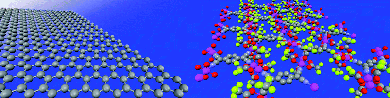 | ||
| Fig. 9 Comparison between the structural simplicity of a graphene single layer (left) and a more complex 2D structure based on a ruthenium based MOF (right). | ||
Acknowledgements
This work was supported by the MICINN (MAT2007-66476-C02-01/02 and CTQ2006-027185-E), Comunidad de Madrid (S2009_MAT-1467), and EU (FP6-029192). C. G. N. thanks the Spanish MEC for funding through the “Ramón y Cajal” program.References and notes
- G. A. Ozin and A. C. Arsenault, Nanochemistry, RSC Publishing, Cambridge, UK, 2005 Search PubMed.
- H. W. Kroto, J. R. Heath, S. C. O'Brien, R. F. Curl and R. E. Smalley, Nature, 1985, 318, 162–163 CrossRef CAS.
- S. Iijima, Nature, 1991, 354, 56–58 CrossRef CAS.
- K. S. Novoselov, A. K. Geim, S. V. Morozov, D. Jiang, Y. Zhang, S. V. Dubonos, I. V. Grigorieva and A. A. Firsov, Science, 2004, 306, 666–669 CrossRef CAS.
- K. S. Novoselov, D. Jiang, F. Schedin, T. J. Booth, V. V. Khotkevich, S. V. Morozov and A. K. Geim, Proc. Natl. Acad. Sci. U. S. A., 2005, 102, 10451–10453 CrossRef CAS.
- A. K. Geim and K. S. Novoselov, Nat. Mater., 2007, 6, 183–191 CrossRef CAS.
- T. A. Land, T. Michely, R. J. Behm, J. C. Hemminger and G. Comsa, Surf. Sci., 1992, 264, 261–270 CrossRef CAS.
- P. W. Sutter, J. I. Flege and E. A. Sutter, Nat. Mater., 2008, 7, 406–411 CrossRef CAS.
- C. Berger, Z. M. Song, T. B. Li, X. B. Li, A. Y. Ogbazghi, R. Feng, Z. T. Dai, A. N. Marchenkov, E. H. Conrad, P. N. First and W. A. de Heer, J. Phys. Chem. B, 2004, 108, 19912–19916 CrossRef CAS.
- J. Sakamoto, J. van Heijst, O. Lukin and A. D. Schluter, Angew. Chem., Int. Ed., 2009, 48, 1030–1069 CrossRef CAS.
- R. Hao, W. Qian, L. H. Zhang and Y. L. Hou, Chem. Commun., 2008, 6576–6578 RSC.
- Y. Hernandez, V. Nicolosi, M. Lotya, F. M. Blighe, Z. Y. Sun, S. De, I. T. McGovern, B. Holland, M. Byrne, Y. K. Gun'ko, J. J. Boland, P. Niraj, G. Duesberg, S. Krishnamurthy, R. Goodhue, J. Hutchison, V. Scardaci, A. C. Ferrari and J. N. Coleman, Nat. Nanotechnol., 2008, 3, 563–568 CrossRef CAS.
- S. Stankovich, D. A. Dikin, G. H. B. Dommett, K. M. Kohlhaas, E. J. Zimney, E. A. Stach, R. D. Piner, S. T. Nguyen and R. S. Ruoff, Nature, 2006, 442, 282–286 CrossRef CAS.
- A. Lerf, H. Y. He, M. Forster and J. Klinowski, J. Phys. Chem. B, 1998, 102, 4477–4482 CrossRef CAS.
- W. W. Cai, R. D. Piner, F. J. Stadermann, S. Park, M. A. Shaibat, Y. Ishii, D. X. Yang, A. Velamakanni, S. J. An, M. Stoller, J. H. An, D. M. Chen and R. S. Ruoff, Science, 2008, 321, 1815–1817 CrossRef CAS.
- V. Lopez, R. S. Sundaram, C. Gomez-Navarro, D. Olea, M. Burghard, J. Gomez-Herrero, F. Zamora and K. Kern, Adv. Mater., 2009, 21, 4683–4686 CAS.
- D. Li, M. B. Muller, S. Gilje, R. B. Kaner and G. G. Wallace, Nat. Nanotechnol., 2008, 3, 101–105 CrossRef CAS.
- G. Eda, G. Fanchini and M. Chhowalla, Nat. Nanotechnol., 2008, 3, 270–274 CrossRef CAS.
- X. Wang, L. J. Zhi and K. Mullen, Nano Lett., 2008, 8, 323–327 CrossRef CAS.
- M. Osada and T. Sasaki, J. Mater. Chem., 2009, 19, 2503–2511 RSC.
- M. A. Bizeto, A. L. Shiguihara and V. R. L. Constantino, J. Mater. Chem., 2009, 19, 2512–2525 RSC.
- R. Z. Ma, Z. P. Liu, L. Li, N. Iyi and T. Sasaki, J. Mater. Chem., 2006, 16, 3809–3813 RSC.
- Z. G. Chen, J. Zou, G. Liu, F. Li, Y. Wang, L. Z. Wang, X. L. Yuan, T. Sekiguchi, H. M. Cheng and G. Q. Lu, ACS Nano, 2008, 2, 2183–2191 CrossRef CAS.
- T. Sasaki, M. Watanabe, H. Hashizume, H. Yamada and H. Nakazawa, J. Am. Chem. Soc., 1996, 118, 8329–8335 CrossRef CAS.
- T. Sasaki, M. Watanabe, H. Hashizume, H. Yamada and H. Nakazawa, Chem. Commun., 1996, 229–230 RSC.
- R. Abe, K. Shinohara, A. Tanaka, M. Hara, J. N. Kondo and K. Domen, Chem. Mater., 1997, 9, 2179–2184 CrossRef CAS.
- M. M. J. Treacy, S. B. Rice, A. J. Jacobson and J. T. Lewandowski, Chem. Mater., 1990, 2, 279–286 CrossRef CAS.
- Y. Omomo, T. Sasaki, L. Z. Wang and M. Watanabe, J. Am. Chem. Soc., 2003, 125, 3568–3575 CrossRef CAS.
- T. W. Kim, E. J. Oh, A. Y. Jee, S. T. Lim, D. H. Park, M. Lee, S. H. Hyun, J. H. Choy and S. J. Hwang, Chem.–Eur. J., 2009, 15, 10752–10761 CrossRef CAS.
- K. Fukuda, I. Nakai, Y. Ebina, R. Z. Ma and T. Sasaki, Inorg. Chem., 2007, 46, 4787–4789 CrossRef CAS.
- K. Fukuda, T. Saida, J. Sato, M. Yonezawa, Y. Takasu and W. Sugimoto, Inorg. Chem., 2010, 49, 4391–4393 CrossRef CAS.
- T. Tanaka, Y. Ebina, K. Takada, K. Kurashima and T. Sasaki, Chem. Mater., 2003, 15, 3564–3568 CrossRef CAS.
- R. E. Schaak and T. E. Mallouk, Chem. Mater., 2000, 12, 3427–3434 CrossRef CAS.
- S. Ida, C. Ogata, M. Eguchi, W. J. Youngblood, T. E. Mallouk and Y. Matsumoto, J. Am. Chem. Soc., 2008, 130, 7052–7059 CrossRef CAS.
- R. E. Schaak and T. E. Mallouk, Chem. Commun., 2002, 706–707 RSC.
- R. E. Schaak and T. E. Mallouk, Chem. Mater., 2000, 12, 2513–2516 CrossRef CAS.
- S. Ida, C. Ogata, U. Unal, K. Izawa, T. Inoue, O. Altuntasoglu and Y. Matsumoto, J. Am. Chem. Soc., 2007, 129, 8956–8957 CrossRef CAS.
- K. Fukuda, K. Akatsuka, Y. Ebina, R. Ma, K. Takada, I. Nakai and T. Sasaki, ACS Nano, 2008, 2, 1689–1695 CrossRef CAS.
- S. Ida, D. Shiga, M. Koinuma and Y. Matsumoto, J. Am. Chem. Soc., 2008, 130, 14038–14039 CrossRef CAS.
- L. F. Hu, R. Z. Ma, T. C. Ozawa and T. Sasaki, Chem.–Asian J., 2010, 5, 248–251 CrossRef CAS.
- R. Z. Ma, Z. P. Liu, K. Takada, N. Iyi, Y. Bando and T. Sasaki, J. Am. Chem. Soc., 2007, 129, 5257–5263 CrossRef CAS.
- C. Janiak, Dalton Trans., 2003, 2781–2804 RSC.
- R. Mas-Balleste, O. Castillo, P. J. S. Miguel, D. Olea, J. Gomez-Herrero and F. Zamora, Eur. J. Inorg. Chem., 2009, 2885–2896 CrossRef CAS.
- J. V. Barth, G. Costantini and K. Kern, Nature, 2005, 437, 671–679 CrossRef CAS.
- Y. M. Lin, K. A. Jenkins, A. Valdes-Garcia, J. P. Small, D. B. Farmer and P. Avouris, Nano Lett., 2009, 9, 422–426 CrossRef CAS.
- L. Welte, U. García-Couceiro, O. Castillo, D. Olea, C. Polop, A. Guijarro, A. Luque, J. M. Gómez-Rodríguez, J. Gómez-Herrero and F. Zamora, Adv. Mater., 2009, 21, 2025–2028 CrossRef CAS.
- L. Welte, R. González-Prieto, D. Olea, M. Rosario Torres, J. L. Priego, R. Jiménez-Aparicio, J. Gómez-Herrero and F. Zamora, ACS Nano, 2008, 2, 2051–2056 CrossRef CAS.
- J. M. J. Paulusse and R. P. Sijbesma, Angew. Chem., Int. Ed., 2004, 43, 4460–4462 CrossRef CAS.
- P. Amo-Ochoa, L. Welte, R. González-Prieto, P. J. Sanz Miguel, C. J. Gómez-García, E. Mateo-Martí, S. Delgado, J. Gómez-Herrero and F. Zamora, Chem. Commun., 2010, 46, 3262–3264 RSC.
- K. D. Oyler, X. L. Ke, I. T. Sines, P. Schiffer and R. E. Schaak, Chem. Mater., 2009, 21, 3655–3661 CrossRef CAS.
- K. S. Novoselov, A. K. Geim, S. V. Morozov, D. Jiang, M. I. Katsnelson, I. V. Grigorieva, S. V. Dubonos and A. A. Firsov, Nature, 2005, 438, 197–200 CrossRef.
- Y. B. Zhang, Y. W. Tan, H. L. Stormer and P. Kim, Nature, 2005, 438, 201–204 CrossRef CAS.
- D. A. Abanin and L. S. Levitov, Science, 2007, 317, 641–643 CrossRef CAS.
- J. R. Williams, L. DiCarlo and C. M. Marcus, Science, 2007, 317, 638–641 CrossRef CAS.
- P. R. Wallace, Phys. Rev., 1947, 71, 622–634 CrossRef CAS.
- J. C. Meyer, A. K. Geim, M. I. Katsnelson, K. S. Novoselov, T. J. Booth and S. Roth, Nature, 2007, 446, 60–63 CrossRef CAS.
- X. Du, I. Skachko, A. Barker and E. Y. Andrei, Nat. Nanotechnol., 2008, 3, 491–495 CrossRef CAS.
- K. S. Novoselov, Z. Jiang, Y. Zhang, S. V. Morozov, H. L. Stormer, U. Zeitler, J. C. Maan, G. S. Boebinger, P. Kim and A. K. Geim, Science, 2007, 315, 1379–1379 CrossRef CAS.
- H. B. Heersche, P. Jarillo-Herrero, J. B. Oostinga, L. M. K. Vandersypen and A. F. Morpurgo, Nature, 2007, 446, 56–59 CrossRef CAS.
- F. Wang, Y. B. Zhang, C. S. Tian, C. Girit, A. Zettl, M. Crommie and Y. R. Shen, Science, 2008, 320, 206–209 CrossRef CAS.
- F. N. Xia, T. Mueller, Y. M. Lin, A. Valdes-Garcia and P. Avouris, Nat. Nanotechnol., 2009, 4, 839–843 CrossRef CAS.
- R. R. Nair, P. Blake, A. N. Grigorenko, K. S. Novoselov, T. J. Booth, T. Stauber, N. M. R. Peres and A. K. Geim, Science, 2008, 320, 1308–1308 CrossRef CAS.
- C. Lee, X. D. Wei, J. W. Kysar and J. Hone, Science, 2008, 321, 385–388 CrossRef CAS.
- J. O. Sofo, A. S. Chaudhari and G. D. Barber, Phys. Rev. B: Condens. Matter Mater. Phys., 2007, 75, 153401 CrossRef.
- D. C. Elias, R. R. Nair, T. M. G. Mohiuddin, S. V. Morozov, P. Blake, M. P. Halsall, A. C. Ferrari, D. W. Boukhvalov, M. I. Katsnelson, A. K. Geim and K. S. Novoselov, Science, 2009, 323, 610–613 CrossRef CAS.
- C. Gomez-Navarro, R. T. Weitz, A. M. Bittner, M. Scolari, A. Mews, M. Burghard and K. Kern, Nano Letters, 2007, 7, 3499–3503 CrossRef CAS.
- I. Gierz, C. Riedl, U. Starke, C. R. Ast and K. Kern, Nano Lett., 2008, 8, 4603–4607 CrossRef CAS.
- C. Gomez-Navarro, M. Burghard and K. Kern, Nano Lett., 2008, 8, 2045–2049 CrossRef CAS.
- A. J. M. Giesbers, U. Zeitler, S. Neubeck, F. Freitag, K. S. Novoselov and J. C. Maan, Solid State Commun., 2008, 147, 366–369 CrossRef CAS.
- X. S. Wu, M. Sprinkle, X. B. Li, F. Ming, C. Berger and W. A. de Heer, Phys. Rev. Lett., 2008, 101, 026801 CrossRef.
- S. Suzuki and M. Miyayama, J. Phys. Chem. B, 2006, 110, 4731–4734 CrossRef CAS.
- L. Z. Wang, K. Takada, A. Kajiyama, M. Onoda, Y. Michiue, L. Q. Zhang, M. Watanabe and T. Sasaki, Chem. Mater., 2003, 15, 4508–4514 CrossRef CAS.
- N. Miyamoto, Y. Yamada, S. Koizumi and T. Nakato, Angew. Chem., Int. Ed., 2007, 46, 4123–4127 CrossRef CAS.
- T. Yui, Y. Kobayashi, Y. Yamada, T. Tsuchino, K. Yano, T. Kajino, Y. Fukushima, T. Torimoto, H. Inoue and K. Takagi, Phys. Chem. Chem. Phys., 2006, 8, 4585–4590 RSC.
- H. Sato, K. Okamoto, K. Tamura, H. Yamada, K. Saruwatari, T. Kogure and A. Yamagishi, Appl. Phys. Express, 2008, 1, 035001 Search PubMed.
- M. Osada, Y. Ebina, K. Takada and T. Sasaki, Adv. Mater., 2006, 18, 295–299 CrossRef CAS.
- Z. P. Liu, R. Z. Ma, M. Osada, N. Iyi, Y. Ebina, K. Takada and T. Sasaki, J. Am. Chem. Soc., 2006, 128, 4872–4880 CrossRef CAS.
- M. Osada, M. Itose, Y. Ebina, K. Ono, S. Ueda, K. Kobayashi and T. Sasaki, Appl. Phys. Lett., 2008, 92, 253110 CrossRef.
- P. Rabu and M. Drillon, Adv. Eng. Mater., 2003, 5, 189–210 CrossRef CAS.
| This journal is © The Royal Society of Chemistry 2011 |