Single exposure fabrication and manipulation of 3D hydrogel cell microcarriers†‡
Lily Nari
Kim
ab,
Sung-Eun
Choi
b,
Junhoi
Kim
b,
Hyoki
Kim
b and
Sunghoon
Kwon
*ab
aSchool of Electrical Engineering and Computer Science, Seoul National University, 599 Gwanak-ro, Gwanak-gu, Seoul, 151-744, Korea. E-mail: skwon@snu.ac.kr
bInter-university Semiconductor Research Center (ISRC), Seoul, 151-744, South Korea
First published on 27th October 2010
Abstract
We present a simple and high-throughput method for fabricating free-floating hydrogel cell microcarriers using single exposure UV patterning. We also demonstrate magnetic manipulation of the free-floating cell microcarriers using a magnetic nanoparticle-embedded structure for an active agitation and a solution exchange.
Cell-based assays play an important role in the drug discovery process.1 There has been an interest in miniaturization and parallelization of cell-based assays in order to deal with enormous chemical libraries.2Cell microarrays have emerged as an attractive solution for extreme miniaturization of cell-based assays.3 Conventional fabrication techniques for cell arrays, multistep soft lithography methods which use a silicon photolithography step followed by fabrication of a PDMS mold and crosslinking of PEG are performed to create hydrogel microwells.4–7 The silicon lithography method is efficient for large scale fabrication of microwells, however, it requires microfabrication facilities and does not allow much flexibility over 3D geometry. Previously 3D polymer lithography techniques such as multiphoton lithography (MPL) and micro-stereolithography (µSL) have been widely used for generating 3D structures.8–12 However, these approaches require complicated techniques in order to create microstructures with specific 3D morphologies such as microcups or microwells. 3D Structures are generated in a voxel-by-voxel or a layer-by-layer fashion. Therefore, the fabrication of cell containers using MPL or µSL is time consuming. In addition, the control of 3D morphology on the micron-scale often requires lithographical methods with small depth of focus (DOF) and limited field of view (FOV), thereby hindering lithography throughput. Consequently, a simple 3D lithography technique for cell microcarrier fabrication, which allows high-throughput fabrication, is necessary.
In this work, we present a simple and high-throughput method for fabricating free-floating cup-shaped microstructures using single exposure UV patterning. In order to enable controlled synthesis, we characterized the modulation of the focus depth by varying the height of the image plane. By selectively focusing the projected image at the desired depth inside the resin, we demonstrate various microstructures with different 3D morphologies using the same mask pattern. The large DOF and FOV of the system allow for high-throughput generation of the 3D structures via the projection-based lithography scheme. The cup-shaped hydrogel microstructures can be used as cell microcarriers. We also demonstrate magnetic manipulation of the free-floating cell microcarriers using a magnetic nanoparticle-embedded structure. Our cell carrier has beneficial magnetic handling capabilities including an active agitation scheme for improved reaction kinetics in microscale environments. Furthermore, magnetic manipulation can be used for active separation of cell carriers from the original solution which can be useful for cell-based assays requiring solution exchange.
As depicted in Fig. 1A and B, free-floating cup-shaped 3D microstructures are fabricated by focusing a projected image at the proper depth into a resin layer. By pulling up the image plane from the bottom to the top of the channel, the geometries of the fabricated particles are changed due to the altered light path and light overlap area. Using this projection UV lithography method, a precisely controlled image with a large DOF allows for single exposure generation of 3D microcup structures.13,14 The prepolymer resin in the UV exposure area polymerizes throughout the cross-section of the channel, so the height of the particle is determined by the height of the channel. The curing depth can be reduced or expanded chemically by varying the amount of photoinitiator in the UV containing resin and physically by varying UV energy.15 To form a microsized cup, a ring pattern is exposed for 0.1 s and the channel is washed with EtOH.
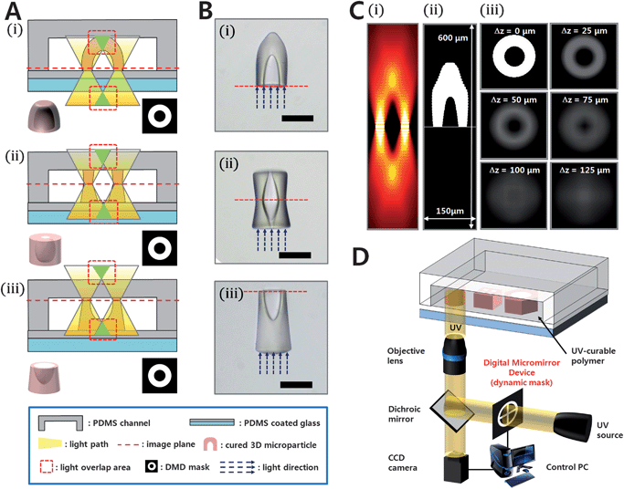 | ||
| Fig. 1 Fabrication of microcups. (A) Schematic illustration of the approach used to manufacture 3D microcups with 3 different morphologies with arbitrary control of focus depth. (B) Bright field images of fabricated 3D microcups with 3 different shapes. All the 3D microstructures are extruded from a same ring-shaped mask pattern. All scale bars indicate 100 µm. (C) Simulation of light propagation. (i) A cross-sectional view of calculated z-dependent intensity distribution of light projected from a ring-shaped object. (ii) Estimation of the particle shape by determining the gel point. (iii) In-plane light intensity distribution; different values of Δz are displayed. (D) The OFML system used for creating 3D microstructures. The OFML system is composed of two parts: the focus-tunable channel and the optical system. | ||
The formation of a cup-shaped structure from a ring-shaped mask can be explained by applying the scalar diffraction theory (see details in the ESI, S4‡).16Fig. 1Ci shows a cross-sectional view of light intensity distribution across x–z plane with the y-axis fixed at the diametral line of the ring-shaped mask pattern. In Fig. 1Cii, the effect of absorption is applied to the range of △z > 0 by setting the z-directional position of the image plane on the surface of substrate. In this way, we can estimate the shapes of microparticles by determining the gel point as shown in Fig. 1Cii.17 In-plane light intensity distributions depending on the variation of △z are calculated with respect to a ring-shaped mask pattern as displayed in Fig. 1Ciii, clearly showing various sectional views of a cup-shaped particle.
Fig. 2 shows various cup-shaped microstructures. A cup-shaped 3D microstructure can be fabricated within a second using the UV projection-based system. In order to fabricate the fluorescent cup-shaped microstructures, ethoxylated trimethylolpropane triacrylate (ETPTA) is used as a photocurable material and RITC- and FITC-embedded silica beads are added to the prepolymer resin. A microcup, a microcup-in-a-cup, and 2 × 2 and 3 × 3 microwell array structures are fabricated using 2D masks and OFML. In order to create the 3D microstructures, each mask pattern is exposed for 0.1 s. The fluorescence images reveal the 3D configuration of the particles.
 | ||
| Fig. 2 (A) Fluorescence images of various cup-shaped 3D microparticles. The prepolymer resin is photopolymerized with fluorescent silica beads. The cross-sectional images reveal the 3D configurations of the particles. (i) The 2 × 2 microwell array. (ii) The microcup. (iii) The 3 × 3 microwell array. (iv) The microcup-in-a-cup. The insets show bright field images of top view. The scale bars indicate 50 µm. (B) A collection of 3D microstructures with micro-cavity. Our method utilizes a projection lithography scheme with low numerical aperture optics which can generate one 3D cup-shaped microstructure in a single exposure by exposing a mask pattern on the entire field of view without scanning through the plane which enables high-throughput fabrication. The scale bar indicates 200 µm. | ||
Using the method depicted in Fig. 3A, we generate hydrogel microcarriers. In order to load cells and polymer microspheres into the micropores, HeLa and T24 cell suspensions, stained with red fluorescence, and a commercial polystyrene (PS) yellow dyed microsphere solution (10 µm, Polysciences) are poured on the hydrogel arrays by pipetting. The cells and polymer beads settle to the bottom of the microwell with almost all of the microwells filled with cells or beads after a single pipetting step. By vortexing mildly in water, microcarriers containing cells come off the glass substrate, and the free-floating hydrogel microcarriers are collected into a microtube. In Fig. 3B and C, the bright and fluorescence images show the 3D configuration of the free-floating microcarriers, where the red HeLa cells and yellow PS beads are placed stably inside the microwells. The fabricated structure is a transparent hydrogel but fluorescence emissions are seen in the fluorescent microscope image. In this method, since cells are not cured with polymer resin, the cells are not damaged by reactive photoinitiators and UV radiation. Therefore the particle can be used as a harmless material carrier. Also since hydrogels are liquid-permeable and have desirable mechanical properties for cell growth, the hydrogel carrier can be used as a reaction chamber for cell-based assays. Although we demonstrate only one particular size of microcarrier for the sake of clarity and consistency, the size and shape of each microwell can be individually controlled by modifying the mask design, magnification, and numerical aperture of the objective lens and intensity of UV.
 | ||
| Fig. 3 (A) Schematic diagram of fabrication steps for 3D hydrogel cell carriers. The 3 × 3 microwell array is fabricated with PEG-DA by exposing a UV pattern between glass substrates. In order to load cells into the hydrogel microcarrier, HeLa and T24 cell suspensions, stained with red fluorescence, and a commercial polystyrene microsphere solution are poured on the hydrogel arrays by pipetting. Almost all of the microwells are filled with cells in a single pipetting step. The hydrogel carriers containing cells or beads are collected into a microtube. (B) Bright field images of a top (i) and cross-sectional view (ii) of a hydrogel carrier containing beads. (C) Fluorescence images of a ‘fluorescent hydrogel carrier’ containing HeLa cells. (D) Bright field images of a ‘magnetic hydrogel carrier’ containing T24 cells. (E) Solution exchange process viamagnetic separation of carriers. (F and G) Optical microscopy sequences (see ESI, S5‡) showing the magnetic manipulation of the magnetic carrier. The scale bars indicate 50 µm (B, C, and D) and 200 µm (F), 100 µm (G). | ||
It is useful to incorporate magnetic materials into the carriers to enable microstructure manipulation and micro-mixing.18,19 Magnetic hydrogel carriers are obtained by curingFe3O4 nanoparticle-embedded PEG-DA under a magnetic field (Fig. 3D).20 The average diameter of the superparamagnetic Fe3O4 nanoparticles is 150 ± 10 nm (see experimental details, an FE-SEM image and magnetic property in the ESI‡). As shown in Fig. 3F, the free-floating magnetic carrier easily moves in the direction of the applied external magnetic field (see ESI, S5‡). The magnetic cell carriers are collected by applying an external magnetic field to a vial containing the carriers which allows solution exchange (Fig. 3E). Since the particle chains are aligned according to the direction of the applied magnetic field, various orientational manipulations of the particles are possible.21 By rotating the external magnetic field horizontally, the carrier rotates around its own vertical axis, allowing for a rapid reaction between the cell and molecules in a solution (see ESI, S5‡). Therefore the manipulation of the free-floating magnetic cell carrier can be useful for cell-based assays involving a chemical reaction and a solution exchange.
In conclusion, we have demonstrated a single exposure method to fabricate 3D polymeric structures by modulating the focus depth using various mask patterns. Our method utilizes a projection lithography scheme with low numerical aperture optics, which can generate 3D particles by exposing a mask pattern on the entire field of view without scanning through the plane. By focusing a projected image at the optimum depth within the resin, cup-shaped microstructures can be generated in less than a second. Although limited to cup-shaped microstructures, this technique is inexpensive and fast compared to conventional 3D fabrication techniques, allowing parallel and high-throughput synthesis of 3D structures. The use of the free-floating 3D microstructures as a carrier enables arbitrary control of cells and solution exchange. Therefore we believe that this 3D microstructure can be useful in various applications, including a material carrier and potentially as a reaction chamber for cell-based assays.
Acknowledgements
This work was supported by the Korea Science and Engineering Foundation (KOSEF) grant funded by the Korean Government (MEST) (2010-007612 and 2010-0017860).Notes and references
- S. Fox, S. Farr-Jones, L. Sopchak, A. Boggs, H. W. Nicely, R. Khoury and M. Biros, J. Biomol. Screening, 2006, 11, 864–869 CrossRef.
- P. S. Dittrich and A. Manz, Nat. Rev. Drug Discovery, 1985, 5, 210–218.
- D. Castel, A. Pitaval, M. A. Debily and X. Gidrol, Drug Discovery Today, 2006, 11, 616–622 CrossRef CAS.
- M. Charnley, M. Textor, A. Khademhosseini and M. P. Lutolf, Integr. Biol., 2009, 1, 625–634 RSC.
- C. Ingham, J. Bomer, A. Sprenkels, A. van den Berg, W. De Voss and J. V. H. Vlieg, Lab Chip, 2010, 10, 1410–1416 RSC.
- J. M. Karp, J. Yeh, G. Eng, J. Fukuda, J. Blumling, K.-Y. Suh, J. Cheng, A. Mahdavi, J. Borenstein, R. Langer and A. Khademhosseini, Lab Chip, 2007, 7, 786–794 RSC.
- M. Cordey, M. Limacher, S. Kobel, V. Taylor and M. P. Lutolf, Stem Cells, 2008, 26, 2586–2594 Search PubMed.
- S. Maruo, O. Nakamura and S. Kawata, Opt. Lett., 1997, 22, 132–134 Search PubMed.
- X. Zhang, X. N. Jiang and C. Sun, Sens. Actuators, A, 1999, 77, 149–156 CrossRef.
- S. Jeon, J.-U. Park, R. Cirelli, S. Yang, C. E. Heitzman, P. V. Braun, P. J. A. Kenis and J. A. Rogers, Proc. Natl. Acad. Sci. U. S. A., 2004, 101, 12428–12433 CrossRef CAS.
- R. Nielson, B. Kaehr and J. Shear, Small, 2009, 5, 120–125 CrossRef CAS.
- F. Claeyssens, E. A. Hasan, A. Gaidukeviciute, D. S. Achilleos, A. Ranella, C. Reinhardt, A. Ovsianikov, X. Shizhou, C. Fotakis, M. Vamvakaki, B. N. Chichkov and M. Farsari, Langmuir, 2009, 25, 3219–3223 CrossRef CAS.
- S. A. Lee, S. E. Chung, W. Park, S. H. Lee and S. Kwon, Lab Chip, 2009, 9, 1670–1675 RSC.
- R. Yang, C. Mullen, M. Schaline, K. Reithmaier and R. Sheets, Microsyst. Technol., 2008, 14, 1233–1243 CrossRef CAS.
- C. Sun, N. Fang, D. M. Wu and X. Zhang, Sens. Actuators, A, 2005, 121, 113–120 CrossRef.
- J. W. Goodman, Introduction to Fourier Optics, Robert & Company Publishers, 2005 Search PubMed.
- P. J. Flory, Principles of Polymer Chemistry, Cornell University Press, 1953 Search PubMed.
- T. G. Leong, C. L. Randall, B. R. Benson, N. Bassik, G. M. Stern and D. H. Gracias, Proc. Natl. Acad. Sci. U. S. A., 2009, 106, 703–708 CrossRef CAS.
- M. S. Sakar, E. B. Steager, D. H. Kim, M. J. Kim, G. J. Pappas and V. Kumar, Appl. Phys. Lett., 2010, 96, 043705 CrossRef.
- H. Kim, J. Ge, J. Kim, S.-E. Choi, H. Lee, H. Lee, W. Park, Y. Yin and S. Kwon, Nat. Photonics, 2009, 3, 534–540 Search PubMed.
- H. Lee, J. Kim, H. Kim, J. Kim and S. Kwon, Nat. Mater., 2010, 9, 745–749 CrossRef CAS.
Footnotes |
| † Published as part of a LOC themed issue dedicated to Korean Research: Guest Editors: Professor Je-Kyun Park and Kahp-Yang Suh. |
| ‡ Electronic supplementary information (ESI) available: Experimental procedure, beam pattern propagation analysis and movie. See DOI: 10.1039/c0lc00369g |
| This journal is © The Royal Society of Chemistry 2011 |