Practical approach for macroporous structure embedded microfluidic system and the catalytic microchemical application†‡
ZuoYi
Xiao§
a,
Yun
Zhao§
a,
Anjie
Wang
a,
Jayakumar
Perumal
b and
Dong-Pyo
Kim
*bc
aState Key Laboratory of Fine Chemicals, Dalian University of Technology, 158 Zhongshan Road, Dalian 116012, People's Republic of China
bCenter of Applied Microfluidic Chemistry, Department of Fine Chemical Engineering and Chemistry, Chungnam National University, Daejeon 305-764, Korea. E-mail: dpkim@cnu.ac.kr; Fax: (+82) 42 823 6665
cGraduate School of Analytical Science and Technology, Chungnam National University, Daejeon 305-764, Korea
First published on 17th November 2010
Abstract
We present a low cost and practical approach to integrate 3D ordered macroporous polyfluoropolyether (PFPE) patterns into a microchannel by a series of porous pattern fabrication processes and subsequent photolithography in a site- and shape-selective manner. The 3D ordered macroporous patterns with high-resolution edges were firstly fabricated by microtransfer molding (μ-TM) of the sacrificial polystyrene (PS) template infiltrated with PFPE as a non-adhesive and solvent-resistant skeletal material. The resulting robust PFPE porous structures with high solvent resistance on a silicon wafer can easily be embedded into the microchannel with the aid of conventional photolithography, leading to a microfluidic system with a built-in microstructure. Moreover, catalyticPd nanoparticles implanted on the surface of the porous structure were obtained by use of Pd nanoparticle deposited PS spheres, the porous structure embedded channel was utilized to perform a Suzuki coupling reaction.
Introduction
Three dimensionally (3D) ordered macroporous materials are of considerable technological and scientific importance owing to their application in wide fields, such as photonic band gap materials,1protein separation,2 chemical sensors,3membranes,4 and catalysts.5 In particular, the integration of porous materials in the microchannel domain is attractive by adding alternative functions into the fundamental advantages of microfluidic chemical systems, such as large surface to volume ratio and excellent mass and heat transfer. Microreaction systems represent a promising way to reduce the cost and time of chemical processes with increased selectivity, safety and sensitivity, further to enhance the analysis signal and reliability in the biological system.Microfluidic systems with porous structure have been fabricated using conventional methods such as bead packing, polymeric foaming, and porous silica monolith from sol–gel process in the microchannel.6,7 Initial attempts to pack the channels with beads were met with limited success due to poor packing and repeatability.8,9 Furthermore, the high densely packed beads resulted in a high pressure drop due to the low void fraction. To address these challenges, porous monoliths with interconnected flow-through pores composed of polymeric foams or silica-based materials were prepared within the channels. However, most of the polymeric foams are problematic with swelling in organic mediums,10 and inorganic porous materials via sol–gel chemistry are critical with fragile cracking due to intrinsic contraction during the gelation and aging process.11,12 Therefore new materials and the methods to fabricate the porous microstructures in the channel are still required for microfluidic chemical synthesis.
Recently, alternative sophisticated methods have been reported to embed highly uniform 3D ordered macroporous structures into the microchannel, such as multi-beam interference lithography,13,14 two-photon polymerization,15 and conformable phase mask lithography.16 Unfortunately, most of these fabrication techniques require high cost equipment to integrate the fine structure into the microchannel.
In this work, we present a low cost and practical method to generate 3D ordered macroporous fluorinated microstructures with mechanical and chemical robustness within microfluidic channels by incorporating top-down and bottom-up fabrication techniques with no use of special equipment. A series of the porous pattern fabrication process and subsequent photolithography in a site- and shape-selective manner is involved for preparing the microstructure embedded microfluidic system. We also demonstrate that the obtained built-in microfluidic device with solvent resistance is useful for organic microchemical reaction by depositing Pd nanoparticles on the inner surface of the porous structure with high surface area.
Materials and methods
Palladium acetate (Pd(OAc)2), styrene monomer, dicumyl peroxide, 2-methoxyethanol, 4-bromobenzonitrile, potassium carbonate, and phenylboronic acid were purchased from Aldrich. Polyvinylpyrrolidone (PVP) was acquired from Fluka. 2,2′-Azo-bis-isobutyrylnitrile (AIBN) was obtained from ACROS Organics. Acrylated perfluoropolyether (PFPE) was synthesized by a published procedure.17Ethanol was acquired from Daejung Chemicals. Polydimethylsiloxane (PDMS) precursor and curing agent (Sylgard 184) were supplied by Dow Corning. All the chemicals were used without further purification. SU-8 photoresist was purchased from MicroChem Corp. Darocur 1173 was obtained from Ciba in Japan.Synthesis of polystyrene (PS) spheres
PS spheres were prepared by a reported procedure.18 In brief, a mixture of 9.7 g styrene monomer, 1.8 g PVP and 0.1 g AIBN was dissolved in a mixed solvent of 8.8 g 2-methoxyethanol and 79 g ethanol, then refluxed at 70 °C for 16 h under mechanical stirring with a speed of 250 rpm in a N2 atmosphere. Then PS spheres with 1.5 μm diameter were homogeneously obtained after centrifugation, washing with ethanol and drying at 60 °C. A suspension of 1 wt% PS spheres was formed by dispersing the centrifuged spheres into a mixture of water and ethanol (volume ratio = 1![[thin space (1/6-em)]](https://www.rsc.org/images/entities/char_2009.gif) :3).
:3).
Fabrication of 3D ordered macroporous polymer patterns
A typical procedure for fabricating 3D ordered macroporous patterns is shown in Fig. 1(A). Briefly, 300 μl of 1 wt% 1.5 μm PS spheres was added into a reservoir connected to inlets of PDMS molds with dimensions of 10 mm long, 30 or 60 μm wide and 70 μm high concave line patterns. By using a directed evaporation-induced self-assembly method, PS spheres in the suspension were arranged into a close-packed structure in the PDMS mold with parallel concave line patterns. The PDMS mold with the PS sphere pre-packed template was gently brought into contact with a 10 μm thick acrylated perfluoropolyether (PFPE) film spin-coated on 30 × 55 mm solid substrates (silicon wafer). The voids among the PS spheres were readily filled with PFPE precursor mixed with 2 wt% photoinitiator within a few minutes. The resulting sample was exposed to 350 nm UV irradiation for a few minutes. Subsequently, the PDMS mold was released from the PS spheres-PFPE composite patterns. The composite patterns on the substrate were dipped into toluene for 12 h at room temperature to remove the sacrificial PS template, then the 3D ordered porous PFPE patterns at 10 × 10 mm size were obtained. | ||
| Fig. 1 Procedure for fabrication of (A) 3D ordered macroporous PFPE patterns, (B) SU-8 microchannel with built-in 3D ordered porous PFPE patterns. | ||
Fabrication of Pd nanoparticle deposited porous structure
Catalytic Pd nanoparticles were prepared by stirring 1 ml ethanol solution mixed with 0.001 g Pd(OAc)2 at room temperature for 1 h as reported.19 Then, a 50 μl suspension including the nanoparticles was dropped into the pre-packed PS sphere template in the PDMS mold and dried for 30 min to deposit the sphere surface with the nanoparticles. The same process was repeated 5 times to increase the deposited concentration of nanoparticles. The nanoparticle deposited PS template was infiltrated with the PFPE precursor, UV exposure, demolding and wet etching processes were performed under identical, aforementioned conditions. Finally, the 3D ordered macroporous PFPE patterns with the entrapped Pd nanoparticles were obtained.Fabrication of porous microstructure embedded microchannel
The 3D macroporous microstructure embedded microchannel was fabricated by a typical photolithographic technique, as shown in Fig. 1(B). The obtained porous PFPE patterns were spin-coated with SU-8 photoresist at 1000 rpm to reach a thickness of 100 μm. After soft baking, the coated film was aligned to be exposed to 365 nm UV irradiation for 10 min through a photomask with an S or Y-shaped pattern with a 500 μm wide channel. Then the 3D porous patterns were embedded into the SU-8 microchannel by developing the unexposed areas after hard baking at 100 °C for 5 min. The photomask design and alignment could be varied for embedding the desired pattern into the microchannel. The 3D ordered porous pattern built-in microchannel was sealed by using a thermally cured PDMS slab after surface activation by oxygen plasma treatment. For comparison, the identical Y-shaped SU-8 microchannel without the built-in microstructure was fabricated by the same route as aforementioned. Then, the Pd nanoparticles were simply deposited on the surface of the microchannel by filling it with the nanoparticle suspension (see Scheme 1S of the ESI‡).Catalytic microchemical reaction of the microstructure embedded microchannel
A Y-shaped microchannel with Pd deposited macroporous polymer structures was used for a Suzuki coupling reaction as depicted at Scheme 1. 145.6 mg (80 mM) of 4-bromobenzonitrile and 248.8 mg (160 mM) of potassium carbonate were diluted to a total volume of 5 ml water and 5 ml ethanol, yielding a mixed solution (denoted as A). Then 146.4 mg (120 mM) of phenylboronic acid was added into 5 ml water and 5 ml ethanol, producing a solution (denoted as B).20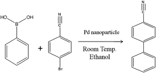 | ||
| Scheme 1 Suzuki reaction for the porous structure embedded microreactor. | ||
The catalytic microchemical reaction was carried out by injecting solutions A and B through two inlets of the Y shaped microchannel at various flow rates 0.5∼5 μl min−1 with two separate syringe pumps. The product solution was collected in 0.5 ml portions prior to measuring the conversion efficiency of the reaction by high performance liquid chromatography (HPLC, Phenomenex).
Characterization
The microstructures were observed by scanning electron microscopy (SEM, JSM-6300/JEOL) and optical microscopy (SV 32, Sometech). High-resolution transmission electron microscope (HRTEM, JEM-2100F, JEOL) images were taken at 200 kV. The solvent resistance of the UV cured PFPE polymer was evaluated by measuring the swelling ratios and the weight change when 10 × 10 × 1 mm sized cured PFPE blocks were dipped for 12 to 24 h in commonly used organic and inorganic solvents. The presence of leached Pd was analyzed using inductively coupled plasma atomic emission spectrometry (ICP-AES, Optima 3300DV/Perkin-Elmer Instruments).Results and discussion
Solvent resistance of the UV cured PFPE
Various porous polymeric microstructures are often insufficient in thermal and chemical stability. In this work, the solvent stability of the PFPE polymer is quite important for enduring the wet-etching and photolithographic developing conditions in the post-fabrication step as well as the microchemical synthetic applications. Herein, the swelling ratio of the cured PFPE blocks was tested by measuring the weight change when dipped into solvents for 12 h and 24 h as shown in Table 1. The samples show the excellent solvent resistance against CHCl3, toluene, acetone, ethanol, and 70% HNO3 in water. These solvents do not induce any weight change or crack formation.It indicates that PFPE has good chemical resistance to be used as a skeletal material for 3D porous microstructure fabrication. It is consistent with reported results that UV cured PFPE was successfully used for an organic solvent resistant microfluidic device.21
Fabrication of 3D ordered macroporous PFPE microstructure
The macroporous microstructures with mechanical and chemical durability were fabricated by a series of packing sacrificial PS beads by capillary force, transferring the patterned beads onto the substrate coated with a non-adhesive fluoropolymer, then UV curing and wet-etching the structure, which leads to a macroporous polymeric structure on the large area. SEM images in Fig. 2A–C show that 1.5 μm PS spheres were homogeneously packed inside a PDMS mold with parallel concave line patterns by a directed evaporation-induced self-assembly method. During the packing process, capillary forces drove the PS spheres in a suspension to flow along the PDMS patterns and arrange into a close-packed structure. The PS sphere-packed template in the 1 × 1 cm PDMS mold was readily formed within a few hours by this means, much shorter than the overnight process by a MIMIC method.5Fig. 2D–I show typical SEM images of the 3D PFPE macroporous microstructures. All the patterns had a well-ordered and defect-free porous structure with high fidelity. The pore diameter of the porous structure was nearly 1.5 μm, indicating little shrinkage during UV curing and wet etching. It can be clearly seen that all the air pores were inter-connected with windows of ∼350 nm. From a cross-sectional side view the external surface of the patterns was also found to be entirely porous with no blocking, which is required for use as catalytic supports or mixers in the microfluidic system. Moreover the aspect ratio of monolithic porous structures could be controlled in the range of 1 to 2 with no flaw or defect. These phenomena indicate that the PFPE-PS sphere composite patterns were extremely well transferred onto the solid substrate during the demolding process. Recently we reported that the PFPE polymer, a pourable liquid at room temperature,17,22 was useful as an UV nanoimprint mold to fabricate the sub-100 nm patterns with a high resolution due to the extremely low surface energy and its elastomeric behaviour. The intrinsically low adhesion nature enables the release of the replicated microstructures easily, without extra surface treatment.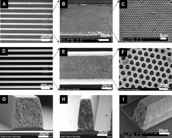 | ||
| Fig. 2 Optical and SEM images of (A–C) PS sphere-packed crystals in the PDMS mold at different magnifications, (D–F) top-views of 3D porous PFPE patterns and (G–I) cross-sectional and side views. | ||
In addition, it is worth noting that the highly viscous PFPE precursor (∼400 cPs) completely filled the confined space of the 70 μm thick PS template in a few minutes under the capillary force. More importantly, the large size of the patterns over a square centimetre facilitates the alignment of the photomask for preparing the microstructure embedded microchannel in a site- and shape-selective manner. In addition, it is worth noting that the void fraction (∼0.74) of the porous system is much higher than that (∼0.26) of the bead packed crystal. Hence, it is expected that the porous system lowered the pressure drop more than the bead pack system, indicating that the viscous fluids can freely flow even at high flow rates throughout the porous channel.23 Moreover, the porous PFPE microstructures functionalized by Pd nanoparticles are shown in Fig. 3. The PS sphere-packed template was modified by dropping a Pd nanoparticle suspension several times, followed by infiltration of the PFPE precursor, UV curing and wet etching.
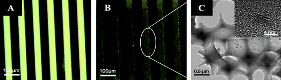 | ||
| Fig. 3 Comparative optical images of 3D ordered porous PFPE structures with (A) no Pd nanoparticles, (B) deposited Pd nanoparticles and (C) TEM images of the PFPE porous structure with immobilized Pd nanoparticles at different magnifications. | ||
Eventually, the Pd nanoparticles were implanted on the inner surface of the porous PFPE microstructure. From optical microscopy images, it was clearly found that the original white color of the porous patterns was changed to a black color, presumably due to the scattering behavior of the deposited nanoparticles.
From TEM images in Fig. 3C, ∼5 nm nanoparticles were immobilized on the surface of the 3D ordered porous structure. In addition, the XPS spectrum showed a peak at binding energy 335.2 eV corresponding to the presence of zero-valent state Pd (Fig. 1S of ESI‡).
Fabrication and microchemical reaction of the microstructure embedded microchannel
In addition to the fabrication of the macroporous pattern, a conventional photolithographic process was employed to fabricate the built-in macroporous microstructure in the microfluidic channel for microchemical application. The mechanical, chemical and thermal durability of the PFPE porous patterns enabled them to retain the monolithic entities during photolithography involving a series of processing steps. For example, the microstructures endured high centrifugal forces at the spin coating step, elevated heat treatments at the soft/hard bake step, and chemical and surface tension effects during the developing process. This economical approach provides an alternative route for the microstructure embedded microchannel to other sophisticated and more expensive approaches as reported previously.13–16,23 Moreover, it should be emphasized that this approach offered a low cost and practical route to integrate the porous microstructures into the desired SU-8 microchannels in a site- and shape-selective manner. Fig. 4A–B demonstrate the fabrication of Y- and S-shaped microchannels with the 3D porous PFPE patterns that were integrated at single and multiple sites on the channel, respectively. The number and the oblique angle of the porous line patterns in the microchannel were easily controlled by aligning the photomask with the channel design, which was important for adjusting the microfluidic performance such as reduced back pressure and high mixing efficiency. In addition, the porous skeletal structures were kept in perfection throughout the photolithographic process as shown in Fig. 4C–D. | ||
| Fig. 4 Optical images of macroporous PFPE pattern embedded SU-8 microchannels. (A) Y-shaped microchannel perpendicularly integrated with 60 lines of PFPE patterns. (B) S-shaped microchannel integrated with 3 bunches of PFPE patterns at an angle of 60°. (C) and (D) SEM images with high magnifications of integrated porous patterns in the Y-shaped microchannel. | ||
Eventually, we carried out a preliminary study on the microfluidic application of the macroporous pattern embedded microchannel. The Y-shaped microchannel with catalyticPd nanoparticles deposited on the surface of the embedded porous structure was utilized to perform a Suzuki coupling reaction after sealing with a PDMS slab. As shown in Fig. 5, the microstructure embedded microchannel revealed highly enhanced conversion of the coupling reaction, compared to the plain microchannel with the same geometry in the absence of porous structure. In particular, the catalytic performance in the built-in microreactor at higher flow rates (i.e. shorter reaction times) was dramatically enhanced, due to the increased surface area and catalyst loading. For example, at a flow rate of 5 ml min−1 of reactants, the built-in microreactor resulted in 40% product yield, while nearly no conversion was observed in the plain microreactor at the same flow rate. Alternatively, under a slightly extended reaction time at 0.5 ml min−1, the built-in reactor nearly produced complete conversion with a 97% product yield, which is in contrast to a 23% yield in the plain reactor under the same conditions. In addition, there was only little deviation of the product yields during repeated reactions for 1 h, and no Pd in the product solution was detected as evidenced by ICP-AES, indicating no leaching of implanted catalyst.
 | ||
| Fig. 5 Comparative conversion in the Suzuki coupling reaction carried out by two types of microreactors. (A) 3D porous PFPE pattern embedded microchannel (■), (B) microchannel with no built-in structure (●). | ||
Conclusions
A novel microfluidic system embedded with monolithic 3D macroporous PFPE patterns has been fabricated by a series of fabrication steps, including preparation of porous patterns. Because of the mechanical and chemical stability of the 3D porous PFPE microstructure, it can be embedded inside an SU-8 microchannel by a site- and shape-selective photolithographic technique, which provides a new concept for fabricating embedded microstructure in microchannels. It was demonstrated that this new microfluidic system was highly effective for enhancing the microchemical performance when decorated with catalyticPd nanoparticles.Acknowledgements
This work was supported by Creative Research Initiatives (Center of Applied Microfluidic Chemistry, Project No. 20100000722) of MEST/KOSEF.Notes and references
- K. Busch and S. Jone, Phys. Rev. E, 1998, 58, 3896–3908 Search PubMed; M. Geissler and Y. Xia, Adv. Mater., 2004, 16, 1249–1269 CrossRef CAS; H. Miguez, E. Chomski, F. Garcia-Santamaria, M. Ibisate, S. John, C. Lopez, F. Meseguer, J. Mondia, G. A. Ozin, O. Toader and H. M. van Driel, Adv. Mater., 2001, 13, 1634–1637 CrossRef CAS; S.-K. Lee, G.-R. Li, J.-H. Moon, S.-M. Yang and D. J. Pine, Adv. Mater., 2006, 18, 2111–2116 CrossRef CAS.
- K. Lewandowski, P. Murer, F. Svec and J. M. J. Frechet, Anal. Chem., 1998, 70, 1629–1638 CrossRef CAS.
- Y. Y. Li, F. Cunin, J. R. Link, T. Gao, R. E. Betts, S. H. Reiver, V. Chin, S. N. Bhatia and M. J. Sailor, Science, 2003, 299, 2045–2047 CrossRef CAS.
- D. T. Mitchell, S. B. Lee, L. Trofin, N. Li, T. K. Nevanen, H. Soderlund and C. R. Martin, J. Am. Chem. Soc., 2002, 124, 11864–11865 CrossRef CAS; P. T. Tanev, M. Chibwe and T. J. Pinnavaia, Nature, 1994, 368, 321–323 CrossRef CAS.
- I.-K. Sung, Christian, M. Mitchell, D.-P. Kim and P. J. A. Kenis, Adv. Funct. Mater., 2005, 15, 1336–1342 CrossRef CAS; G. Guan, R. Zapf, G. Kolb, Y. Men, V. Hessel, H. Loewe, J. Ye and R. Zentel, Chem. Commun., 2007, 260–262 RSC; Christian, M. Mitchell, D.-P. Kim and P. J. A. Kenis, J. Catal., 2006, 241, 235–242 CrossRef.
- W. Zhan, G. H. Seong and R. M. Crooks, Anal. Chem., 2002, 74, 4647–4652 CrossRef CAS.
- A. E. Kadib, R. Chimenton, A. Sachse, F. Fajula, A. Galarneau and B. Coq, Angew. Chem., Int. Ed., 2009, 48, 4969–4972 CrossRef CAS.
- R. D. Oleschuk, L. L. Shultz-Lockyear, Y. B. Ning and D. J. Harrison, Anal. Chem., 2000, 72, 585–590 CrossRef CAS.
- A. B. Jemere, R. D. Oleschuk, F. Ouchen, F. Fajuyigbe and D. J. Harrison, Electrophoresis, 2002, 23, 3537–3544 CrossRef CAS.
- N. T. S. Phan, D. H. Brown and P. Styring, Green Chem., 2004, 6, 526–532 RSC; S. J. Haswell, B. O. Sullivan and P. Styring, Lab Chip, 2001, 1, 164–166 RSC.
- J. Kang, D. Wistuba and V. Schurig, Electrophoresis, 2002, 23, 1116–1120 CrossRef CAS.
- J. Babin, J. Iapichella, B. Lefevre, C. Biolley, J.-P. Bellat, F. Fajula and A. Galarneau, New J. Chem., 2007, 31, 1907–1917 RSC.
- M. Campbell, D. N. Sharp, M. T. Harrison, R. G. Denning and A. J. Turberfield, Nature, 2000, 404, 53–56 CrossRef CAS.
- S. Yang, M. Megens, J. Aizenberg, P. Wiltzius, P. M. Chaikin and W. B. Russel, Chem. Mater., 2002, 14, 2831–2833 CrossRef CAS.
- T. A. Pham, D.-P. Kim, T.-W. Lim, S.-H. Park, D.-Y. Yang and K.-S. Lee, Adv. Funct. Mater., 2006, 16, 1235–1241 CrossRef CAS.
- S.-W. Jeon, J.-U. Park, R. Cirelli, S. Yang, C. E. Hitzman, P. V. Braun, P. J. A. Kenis and J. A. Rogers, Proc. Natl. Acad. Sci. U. S. A., 2004, 101, 12428–12433 CrossRef CAS.
- J. Perumal, D.-P. Kim and J.-J. Lee, J. Nanosci. Nanotechnol., 2008, 8, 5341–5346 CrossRef CAS.
- Z. Y. Xiao, A. Wang, J. Perumal and D.-P. Kim, Adv. Funct. Mater., 2010, 20, 1473–1479 CrossRef CAS.
- L. Groschel, R. Haidar, A. Beyer, K.-H. Reichert and R. Schomacker, Catal. Lett., 2004, 95, 67–75 CrossRef.
- C. Basheer, F. S. J. Hussain, H. K. Lee and S. Valiyaveettil, Tetrahedron Lett., 2004, 45, 7297–7300 CrossRef CAS.
- J. P. Rolland, R. M. Van Dam, D. A. Schorzman, S. R. Quake and J. M. Desimone, J. Am. Chem. Soc., 2004, 126, 2322–2323 CrossRef CAS.
- J. Perumal, T.-H. Yoon, H.-S. Jang, J.-J. Lee and D.-P. Kim, Nanotechnology, 2009, 20, 055704 CrossRef.
- S. Park, S. K. Lee, J. H. Moon and S.-M. Yang, Lab Chip, 2009, 9, 3144–3150 RSC.
Footnotes |
| † Published as part of a LOC themed issue dedicated to Korean Research: Guest Editors: Professor Je-Kyun Park and Kahp-Yang Suh. |
| ‡ Electronic supplementary information (ESI) available: XPS spectrum of Pd immobilized on the porous PFPE structure; comparative catalytic microchemical reactions; HPLC measurement of Suzuki coupling reaction product. See DOI: 10.1039/c0lc00108b |
| § ZuoYi Xiao and Yun Zhao worked at Prof. Kim's lab under a co-advisor program. |
| This journal is © The Royal Society of Chemistry 2011 |